US5548671A - Programmable, differential wavelength discriminator - Google Patents
Programmable, differential wavelength discriminator Download PDFInfo
- Publication number
- US5548671A US5548671A US08/322,140 US32214094A US5548671A US 5548671 A US5548671 A US 5548671A US 32214094 A US32214094 A US 32214094A US 5548671 A US5548671 A US 5548671A
- Authority
- US
- United States
- Prior art keywords
- wavelength
- grating
- optical
- discriminator
- waveguides
- Prior art date
- Legal status (The legal status is an assumption and is not a legal conclusion. Google has not performed a legal analysis and makes no representation as to the accuracy of the status listed.)
- Expired - Lifetime
Links
Images


Classifications
-
- G—PHYSICS
- G02—OPTICS
- G02B—OPTICAL ELEMENTS, SYSTEMS OR APPARATUS
- G02B6/00—Light guides; Structural details of arrangements comprising light guides and other optical elements, e.g. couplings
- G02B6/10—Light guides; Structural details of arrangements comprising light guides and other optical elements, e.g. couplings of the optical waveguide type
- G02B6/12—Light guides; Structural details of arrangements comprising light guides and other optical elements, e.g. couplings of the optical waveguide type of the integrated circuit kind
- G02B6/12007—Light guides; Structural details of arrangements comprising light guides and other optical elements, e.g. couplings of the optical waveguide type of the integrated circuit kind forming wavelength selective elements, e.g. multiplexer, demultiplexer
-
- G—PHYSICS
- G02—OPTICS
- G02B—OPTICAL ELEMENTS, SYSTEMS OR APPARATUS
- G02B6/00—Light guides; Structural details of arrangements comprising light guides and other optical elements, e.g. couplings
- G02B6/10—Light guides; Structural details of arrangements comprising light guides and other optical elements, e.g. couplings of the optical waveguide type
- G02B6/12—Light guides; Structural details of arrangements comprising light guides and other optical elements, e.g. couplings of the optical waveguide type of the integrated circuit kind
- G02B2006/12133—Functions
- G02B2006/12164—Multiplexing; Demultiplexing
Definitions
- This invention relates to optical waveguides and more particularly such waveguides capable of providing programmable wavelength discrimination.
- optical fibers and waveguides The range of wavelengths propagated by optical fibers and waveguides is such that this medium is well suited to broadband, long haul communications.
- Optical fibers for example, have a low loss window in the 1.3 to 1.55 ⁇ m range such that properly designed optical transmission systems can transfer optical signals over long distances without intermediate repeaters.
- optical fibers can transmit bandwidths at or approaching the Tera bit range, limitations such as electronic circuitry prevent full utilization of this characteristic. Thus, to more fully exploit this bandwidth capability, it is known to divide the optimum wavelength range into wavelength channels and to impress multiple data streams onto those channels.
- WDM wavelength division multiplexing
- tunable laser transmitters can be tuned to different wavelengths and data transmission from each transmitter is mixed together optically on a fiber. At the receiver end the transmission is separated again using fixed wavelength discriminating optical filters and conventional photodetectors. In this system switching is achieved simply by tuning each transmitter to the wavelength of the intended receiver, rather like a broadcast radio system but in reverse. In other such systems of this kind both the transmitter and receiver or the receiver alone can be tuned over a range of wavelengths.
- optical devices capable of changing the wavelength of light, can be used.
- wavelength division in switching is analogous to the Code Division Multiplex System (CDMA or "spread spectrum" technique used in certain mobile radio telephone systems.
- CDMA Code Division Multiplex System
- each channel transmitted into the optical bus contains a number of wavelengths in a pattern that is different from the pattern of every other transmitter.
- Reception of a selected channel is achieved by correlation of the expected pattern (spectrum shape) with the received signal which contains both the desired pattern as well as all other transmissions.
- the spectral pattern By a proper choice of the spectral pattern, one can achieve separation of the desired signal because all other signals appear as noise. In effect the noise has a low correlation coefficient with the expected pattern while the desired signal exhibits a high correlation.
- optical systems have relied on free space optics with gratings and lenses followed by semiconductor detectors. Spatial wavelength separation has been accomplished by integrated waveguide optics relying on the diffractive effect of multi-path interference.
- Other prior art optical components have relied on light coupling through index matching of parallel waveguides as well as programmable holograms and acousto-optical tunable filters.
- the present invention seeks to provide a class of devices which simplifies the detection and discrimination of optical signals at different wavelengths in a programmable and integrated way.
- the invention also seeks to provide such devices utilizing integrated circuit manufacturing methods which are well understood for high volume manufacturing of precision parts.
- a wavelength discriminator having a waveguide adapted to receive an optical signal on a carrier of a discrete wavelength.
- a grating having a pre-selecting grating period is on the waveguide, the grating period being selected to reflect the discrete wavelength.
- a receiving means is associated with the grating to receive the wavelength reflected by the grating.
- the waveguide is adapted to receive an optical signal having a plurality of wavelengths while the grating is selected to reflect only one of the plurality of wavelengths.
- the discriminator is provided with a pair of waveguides and an upstream optical switch to programmably direct the optical signal to one of the waveguides, At least one of the waveguides is provided with a grating to reflect a preselected one of the plurality of wavelengths to its associated receiving means,
- wavelength discriminators are connected in cascade so that several or all of the wavelengths in the incoming optical signal can be received by individual receivers.
- the receivers are photodetectors.
- a method of isolating an optical carrier of a selected wavelength from an optical signal containing a plurality of optical carriers of different wavelengths comprises launching the optical signal into a waveguide which is provided with an optical grating having a grating period to reflect the selected wavelength.
- the optical signal is caused to propagate through the grating whereby the selected wavelength is separated from the stream of wavelengths.
- a receiver in association with the grating accepts the selected wavelength for further processing.
- the receiver may comprise an optical detector or a second grating of the same period as the first so as to reflect the selected wavelength into a receiving waveguide.
- the method also extends to the isolation and detection of two or more carriers of different, selected wavelengths from the multi-carrier optical signal.
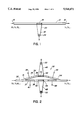
- FIG. 1 is a plan view of a basic wavelength discriminator
- FIG. 2 is a plan view of a dual-waveguide wavelength discriminator
- FIG. 3 is a plan view of wavelength discriminators in cascade
- FIG. 4 is a plan view of wavelength discriminators in cascade having receiving waveguides
- FIG. 5 is a representation of a cascaded discriminator in a rectangular path
- FIG. 6 is a representation of a cascaded discriminator in a zig-zag path.
- FIG. 7 is a representation of a cascaded discriminator in a spiral path.
- a waveguide 12 is configured to receive and transfer therethrough an optical signal including a plurality of wavelengths ⁇ 0 , ⁇ 1 , ⁇ 2 , . . . ⁇ n .
- the waveguide 12 is of a single mode configuration fabricated from suitable electro-optic, acousto-optic or photo-refractive materials.
- suitable electro-optic, acousto-optic or photo-refractive materials Of particular interest in this regard is Lithium Niobate, silicon, glass, etc., and more particularly, semiconductor materials such as III-V alloys, the latter being of interest because it can be processed by well-known semiconductor processing procedures and because of possible integration with photodetectors, optical amplifiers and other optoelectronic components.
- Waveguide 12 has an input end 14 and an output or exit end 16. Spaced between opposite ends of the waveguide is a Bragg reflector 18 comprising a plurality of perturbations formed by well-known means such as wet etching. It is within the scope of the present invention to generate the diffraction gratings in other ways such as: electro-optic effect; thermal effect; acousto-optic effect; or holographic effect.
- the period of the perturbations on the grating 18 is selected to reflect a chosen wavelength.
- a waveguide such as tapered waveguide 20 which confines the reflected light into a narrow region 22 where, in one embodiment, it is detected by photodetector 24.
- the grating has a period ⁇ 0 which reflects wavelength ⁇ 0 .
- the remaining wavelength carriers ⁇ 1 , ⁇ 2 , . . . ⁇ n continue through the waveguide 12 to exit through end 16.
- FIG. 2 illustrates a wavelength discriminator 30 having the capability of optionally isolating more than one wavelength carrier from the range of carriers launched into the discriminator.
- an optical switch in the form of a Y-branch guide is formed at the input end of the device.
- the optical switch 31 has a single input end 32 and a pair of branch arms 34,36.
- Branch arms 34 is coupled to a first waveguide 38 and branch arm 36 is coupled to a second waveguide 40.
- the branch arms are provided with electro-optic means 35,37 respectively to permit the refractive index of each branch to be varied.
- the electro-optic means in a preferred embodiment comprise electrical contacts and terminals 39,41 respectively to allow a biasing voltage or current (positive and/or negative) to be applied independently to each arm.
- the switch without bias voltage or current, functions as a 3-dB coupler so that an optical signal ⁇ 0 , ⁇ 1 , ⁇ 2 , . . . ⁇ n launched into the switch is divided substantially equally between the two arms. If, however, a bias is applied to arm 34 the refractive index of this arm will decrease and the beam or optical signal is switched into branch arm 36. Conversely, if a bias is applied to arm 36, the optical signal is switched to arm 34.
- FIG. 2 shows an optical switch in the form of a Y-branch guide it is to be understood the Other switches such as directional couplers, X-switches, or "normally on" Y-branch switches can also be used.
- a "normally on” switch has a straight through arm with an electrode and a branch arm without an electrode. Without voltage applied to the electrode, light goes through the straight arm. With voltage applied light is switched to the branch arm.
- a grating may be incorporated in one or both of the waveguides. Further, the grating can have the same or different period ⁇ . In the case of a grating in only one waveguide, the period may be selected to reflect, for subsequent detection, only a single wavelength of interest. Thus the wavelength can be isolated by switching the optical signal through the waveguide with the grating. If no isolation is required the optical signal is propagated through the waveguide with no grating.
- a second option is to incorporate gratings in both waveguides such as waveguide 38,40 which have 45 degree reflecting gratings 42,44 respectively (FIG. 2).
- the period ⁇ of each grating may be different such that one grating will reflect one of the wavelength of the optical signal and the other grating will reflect another wavelength.
- grating 42 could have a period ⁇ 0 and grating 44 a period ⁇ 1 such that grating 42 reflects ⁇ 0 and grating 44 reflects ⁇ 1 .
- associated with each grating 42,44 is a tapered waveguide 46,48 respectively.
- the tapered waveguides 46,48 direct the reflected wavelength to photodetectors 50,52 respectively.
- the incoming optical signal may be directed to either waveguide wherein the desired wavelength is isolated from the range of wavelength carriers which make up the optical signal.
- the remaining wavelengths pass through the waveguides and exit the device via exit Y-branch unit 54.
- the waveguides are united at the exit end by a Y-branch combiner 54.
- the combiner may also be provided with electro-optical means such as contacts 56,58 to facilitate the transfer of the optical signal through the discriminator.
- electro-optical means such as contacts 56,58 to facilitate the transfer of the optical signal through the discriminator.
- discriminators such as those shown in FIG. 2 can be connected in cascade as illustrated in FIG. 3.
- the reflecting grating of each discriminator will have a different period, each selected to preferentially reflect one of the many wavelengths which make up the composite optical signal.
- the optical signal launched into the structure comprises wavelengths ⁇ 0 , ⁇ 1 , ⁇ 2 and ⁇ 3 .
- the period of the grating in the first unit 120 is ⁇ 0 which reflects ⁇ 0 .
- this wavelength is detected by detector 122.
- the grating period of the second unit 130 is ⁇ 1 and ⁇ 1 is thus detected by detector 132.
- the third and fourth units 140,150 are configured to detect ⁇ 2 and ⁇ 3 so that all of the wavelengths on the optical signal are detected individually. It will be apparent to one skilled in the art that the combinations of the wavelengths in either side can be achieved arbitrarily by choosing different biasing combinations in each unit. It is also within the scope of the invention to interconnect the detectors on one or both sides to give a sum of the photocurrent for selected wavelengths. This application is comparable to a programmable mask in CDMA.
- the cascaded arrangement of FIG. 3 is configured such that the gratings in both waveguides within a discriminator unit have the same period.
- the portion of the signal propagating through the un-selected waveguide having the selected wavelength can be detected and appropriately processed; i.e., it can be added to or subtracted from the detected signal in the selected waveguide.
- FIG. 4 Another embodiment of the present invention is illustrated in FIG. 4.
- the photodetectors associated with each tapered waveguide as discussed in relation to FIG. 3 are replaced with gratings 222,232,242,252 each having the same period as the associated grating in the waveguide.
- This additional grating has an angle of reflection so as to direct the reflected wavelength into second waveguides 210,212.
- the angle of reflection of the second grating is 45° so that the second waveguides 210,212 are parallel to the main waveguide.
- the reflecting gratings 222,232,242,252 can also be configured such that the beam propagates in the second waveguide 210 or 212 codirectional with the optical signal although it is to be understood that the reflected light can be directed in an contra-directional path.
- the discriminator can be programmed to multiplex selected wavelengths in one waveguide and all remaining wavelengths in the other.
- one side of the cascaded device can have a collector waveguide as shown in FIG. 4 while the other side has photodetectors as shown in FIG. 3.
- the discriminator can be a square or rectangular path with corner mirrors 310 as shown in FIG. 5, zig-zag with mirrors 312 as shown in FIG. 6 or spiral as shown in FIG. 7.
- the discriminator can be programmed to separate the two wavelengths that constitute a bitstream and subtract their intensities from each other to provide a differential decoding function.
- an integrated receiver for a number of optically multiplexed bitstreams can be provided.
- a discriminator of the present invention configured to contain a serial or parallel cascade of several sections provides a means of creating a tunable receiver which can be rapidly reprogrammed to receive different wavelengths.
- the discriminator of the present invention provides a method of automatically collecting all wavelengths of interest in one detector, and all wavelengths of the unwanted signal in a second detector for subsequent comparison and decoding. This is done in a way that permits electronic programming of the desired wavelength sets. It is to be understood, however, that such variations and further examples will fall within the scope of the invention as defined by the appended claims.
Landscapes
- Physics & Mathematics (AREA)
- Engineering & Computer Science (AREA)
- Microelectronics & Electronic Packaging (AREA)
- General Physics & Mathematics (AREA)
- Optics & Photonics (AREA)
- Optical Integrated Circuits (AREA)
Abstract
Description
Claims (10)
Priority Applications (1)
| Application Number | Priority Date | Filing Date | Title |
|---|---|---|---|
| US08/322,140 US5548671A (en) | 1994-10-13 | 1994-10-13 | Programmable, differential wavelength discriminator |
Applications Claiming Priority (1)
| Application Number | Priority Date | Filing Date | Title |
|---|---|---|---|
| US08/322,140 US5548671A (en) | 1994-10-13 | 1994-10-13 | Programmable, differential wavelength discriminator |
Publications (1)
| Publication Number | Publication Date |
|---|---|
| US5548671A true US5548671A (en) | 1996-08-20 |
Family
ID=23253612
Family Applications (1)
| Application Number | Title | Priority Date | Filing Date |
|---|---|---|---|
| US08/322,140 Expired - Lifetime US5548671A (en) | 1994-10-13 | 1994-10-13 | Programmable, differential wavelength discriminator |
Country Status (1)
| Country | Link |
|---|---|
| US (1) | US5548671A (en) |
Cited By (2)
| Publication number | Priority date | Publication date | Assignee | Title |
|---|---|---|---|---|
| US6714575B2 (en) * | 2001-03-05 | 2004-03-30 | Photodigm, Inc. | Optical modulator system |
| GB2537675A (en) * | 2015-04-24 | 2016-10-26 | Qioptiq Ltd | Waveguide for multispectral fusion |
Citations (9)
| Publication number | Priority date | Publication date | Assignee | Title |
|---|---|---|---|---|
| US4747654A (en) * | 1983-05-19 | 1988-05-31 | Yi Yan Alfredo | Optical monomode guidance structure including low resolution grating |
| US4820009A (en) * | 1987-08-13 | 1989-04-11 | Trw Inc. | Electrooptical switch and modulator |
| US4860294A (en) * | 1987-03-30 | 1989-08-22 | Siemens Aktiengesellschaft | Integrated-optical arrangement for bidirectional optical message or signal transmission |
| US4938553A (en) * | 1987-03-16 | 1990-07-03 | Siemens Aktiengesellschaft | Arrangement for an integrated optical spectrometer and the method for manufacturing the spectrometer |
| US5363226A (en) * | 1992-04-06 | 1994-11-08 | Eastman Kodak Company | Apparatus and method for dispersion compensation for a grating coupler using a surface relief reflection grating |
| US5434702A (en) * | 1992-03-04 | 1995-07-18 | Northern Telecom Limited | Optical repeaters |
| US5469520A (en) * | 1994-09-30 | 1995-11-21 | United Technologies Corporation | Compression-tuned fiber grating |
| US5473714A (en) * | 1994-04-29 | 1995-12-05 | At&T Corp. | Optical fiber system using tapered fiber devices |
| US5475780A (en) * | 1993-06-17 | 1995-12-12 | At&T Corp. | Optical waveguiding component comprising a band-pass filter |
-
1994
- 1994-10-13 US US08/322,140 patent/US5548671A/en not_active Expired - Lifetime
Patent Citations (9)
| Publication number | Priority date | Publication date | Assignee | Title |
|---|---|---|---|---|
| US4747654A (en) * | 1983-05-19 | 1988-05-31 | Yi Yan Alfredo | Optical monomode guidance structure including low resolution grating |
| US4938553A (en) * | 1987-03-16 | 1990-07-03 | Siemens Aktiengesellschaft | Arrangement for an integrated optical spectrometer and the method for manufacturing the spectrometer |
| US4860294A (en) * | 1987-03-30 | 1989-08-22 | Siemens Aktiengesellschaft | Integrated-optical arrangement for bidirectional optical message or signal transmission |
| US4820009A (en) * | 1987-08-13 | 1989-04-11 | Trw Inc. | Electrooptical switch and modulator |
| US5434702A (en) * | 1992-03-04 | 1995-07-18 | Northern Telecom Limited | Optical repeaters |
| US5363226A (en) * | 1992-04-06 | 1994-11-08 | Eastman Kodak Company | Apparatus and method for dispersion compensation for a grating coupler using a surface relief reflection grating |
| US5475780A (en) * | 1993-06-17 | 1995-12-12 | At&T Corp. | Optical waveguiding component comprising a band-pass filter |
| US5473714A (en) * | 1994-04-29 | 1995-12-05 | At&T Corp. | Optical fiber system using tapered fiber devices |
| US5469520A (en) * | 1994-09-30 | 1995-11-21 | United Technologies Corporation | Compression-tuned fiber grating |
Non-Patent Citations (16)
| Title |
|---|
| "A Very Low Operation Current InGaAsP/InP Total Internal Reflection Optical Switch Using p/n/p/n Current Blocking Layers", Oh et al, IEEE Photonics Technology Letter, vol. 6, No. 1, Jan. 1994, pp. 65-67. |
| "Digital Optical Switch", Silberberg et al, Appl. Lett., 51(16), 19 Oct. 1987, pp. 1230-1232. |
| "First Digital Optical Switch Based On InP/GaInAsP Double Heterostructure Waveguides", Cavailles et al, Electronics Letters, 25th Apr. 1991, vol. 27, No. 9, pp. 699-700. |
| "Integrated Grating Circuit for Guided-Beam Multiple Division Fabricated by Electron-Beam Direct Writing", Handa et al, Optics Letters, Jul. 1980, vol. 5, No. 7, pp. 309-311. |
| "Integrated Optics 4x4 Switch Matrix With Digital Optical Switches", Granestrand et al, Electronics Letters, 4th Jan. 1990, vol. 26, No. 1, pp. 4-5. |
| "Integrated Optics Components and Devices Using Periodic Structures", Suhara et al, IEEE Journal of Quantum Electronics, vol. QE-22, No. 6, pp. 845-867, Jun. 1986. |
| "Low-Crosstalk 2x2 Digital Optical Switch", Okayama et al, Electronics Letters, 3rd Mar. 1994, vol. 30, No. 5, pp. 403-405. |
| "Monolithic Integrated Microgratings and Photodiodes for Wavelength Demultiplexing", Suhara et al, Appl. Phys. Lett., 40(2), 15 Jan. 1982, pp. 120-122. |
| A Very Low Operation Current InGaAsP/InP Total Internal Reflection Optical Switch Using p/n/p/n Current Blocking Layers , Oh et al, IEEE Photonics Technology Letter, vol. 6, No. 1, Jan. 1994, pp. 65 67. * |
| Digital Optical Switch , Silberberg et al, Appl. Lett., 51(16), 19 Oct. 1987, pp. 1230 1232. * |
| First Digital Optical Switch Based On InP/GaInAsP Double Heterostructure Waveguides , Cavailles et al, Electronics Letters, 25th Apr. 1991, vol. 27, No. 9, pp. 699 700. * |
| Integrated Grating Circuit for Guided Beam Multiple Division Fabricated by Electron Beam Direct Writing , Handa et al, Optics Letters, Jul. 1980, vol. 5, No. 7, pp. 309 311. * |
| Integrated Optics 4x4 Switch Matrix With Digital Optical Switches , Granestrand et al, Electronics Letters, 4th Jan. 1990, vol. 26, No. 1, pp. 4 5. * |
| Integrated Optics Components and Devices Using Periodic Structures , Suhara et al, IEEE Journal of Quantum Electronics, vol. QE 22, No. 6, pp. 845 867, Jun. 1986. * |
| Low Crosstalk 2x2 Digital Optical Switch , Okayama et al, Electronics Letters, 3rd Mar. 1994, vol. 30, No. 5, pp. 403 405. * |
| Monolithic Integrated Microgratings and Photodiodes for Wavelength Demultiplexing , Suhara et al, Appl. Phys. Lett., 40(2), 15 Jan. 1982, pp. 120 122. * |
Cited By (6)
| Publication number | Priority date | Publication date | Assignee | Title |
|---|---|---|---|---|
| US6714575B2 (en) * | 2001-03-05 | 2004-03-30 | Photodigm, Inc. | Optical modulator system |
| GB2537675A (en) * | 2015-04-24 | 2016-10-26 | Qioptiq Ltd | Waveguide for multispectral fusion |
| GB2537675B (en) * | 2015-04-24 | 2018-10-17 | Qioptiq Ltd | Waveguide for multispectral fusion |
| US10191262B2 (en) | 2015-04-24 | 2019-01-29 | Qioptiq Limited | Waveguide for multispectral fusion |
| US20190113725A1 (en) * | 2015-04-24 | 2019-04-18 | Qioptiq Limited | Waveguide for Multispectral Fusion |
| US10598910B2 (en) | 2015-04-24 | 2020-03-24 | Qioptiq Limited | Waveguide for multispectral fusion |
Similar Documents
| Publication | Publication Date | Title |
|---|---|---|
| EP0638837B1 (en) | Device for extraction and re-insertion of an optical carrier in optical communications networks | |
| Ishio et al. | Review and status of wavelength-division-multiplexing technology and its application | |
| US5808763A (en) | Optical demultiplexor | |
| US5982518A (en) | Optical add-drop multiplexers compatible with very dense WDM optical communication systems | |
| US6281977B1 (en) | Interferometric optical device including an optical resonator | |
| US12468099B2 (en) | Polarization diverse receiver with delays | |
| JPH11507738A (en) | Optoelectronic circuit | |
| EP0613263A1 (en) | Optical network comprising a compact wavelength-dividing component | |
| US4571024A (en) | Wavelength selective demultiplexer tuner | |
| EP1225461A2 (en) | Bidirectional multiplexer and demultiplexer based on a single echelle waveguide grating | |
| CA2613105C (en) | Method and system for hitless tunable optical processing | |
| US5054873A (en) | High density integrated optical multiplexer/demultiplexer | |
| US20040005115A1 (en) | Optoelectronic add/drop multiplexer | |
| US6516112B1 (en) | Optical wavelength filter and demultiplexer | |
| US5548671A (en) | Programmable, differential wavelength discriminator | |
| US6671430B2 (en) | Optical device, terminal apparatus, and system for wavelength division multiplexing | |
| EP0984311A2 (en) | Optical multiplexor/demultiplexor | |
| US6549701B1 (en) | Selectable wavelength channel filter for optical WDM systems | |
| US7072538B1 (en) | Planar reconfigurable optical add/drop module | |
| GB2170322A (en) | Integrated optical device with wavelength-selective reflection | |
| US6529302B1 (en) | Channel switching in wavelength encoded optical communication systems | |
| KR100264950B1 (en) | Wavelength-variable light extraction / transmission filter for WDM communication without feedback noise | |
| KR19990020073A (en) | Wavelength-variable optical drop / pass filter system structure for wavelength division multiple communication | |
| JPH01108530A (en) | Optical driving type switch | |
| CA2211644C (en) | Optical demultiplexor |
Legal Events
| Date | Code | Title | Description |
|---|---|---|---|
| AS | Assignment |
Owner name: BELL-NORTHERN RESEARCH LTD., CANADA Free format text: ASSIGNMENT OF ASSIGNORS INTEREST;ASSIGNORS:WU, CHI;MUNTER, ERNST AUGUST;REEL/FRAME:007213/0538 Effective date: 19941004 Owner name: NORTHERN TELECOM LIMITED, CANADA Free format text: ASSIGNMENT OF ASSIGNORS INTEREST;ASSIGNOR:BELL-NORTHERN RESEARCH LTD.;REEL/FRAME:007213/0540 Effective date: 19941108 |
|
| STCF | Information on status: patent grant |
Free format text: PATENTED CASE |
|
| FEPP | Fee payment procedure |
Free format text: PAYOR NUMBER ASSIGNED (ORIGINAL EVENT CODE: ASPN); ENTITY STATUS OF PATENT OWNER: LARGE ENTITY |
|
| AS | Assignment |
Owner name: NORTEL NETWORKS CORPORATION, CANADA Free format text: CHANGE OF NAME;ASSIGNOR:NORTHERN TELECOM LIMITED;REEL/FRAME:010567/0001 Effective date: 19990429 |
|
| FPAY | Fee payment |
Year of fee payment: 4 |
|
| AS | Assignment |
Owner name: NORTEL NETWORKS LIMITED, CANADA Free format text: CHANGE OF NAME;ASSIGNOR:NORTEL NETWORKS CORPORATION;REEL/FRAME:011195/0706 Effective date: 20000830 Owner name: NORTEL NETWORKS LIMITED,CANADA Free format text: CHANGE OF NAME;ASSIGNOR:NORTEL NETWORKS CORPORATION;REEL/FRAME:011195/0706 Effective date: 20000830 |
|
| FPAY | Fee payment |
Year of fee payment: 8 |
|
| FPAY | Fee payment |
Year of fee payment: 12 |
|
| AS | Assignment |
Owner name: CIENA LUXEMBOURG S.A.R.L.,LUXEMBOURG Free format text: ASSIGNMENT OF ASSIGNORS INTEREST;ASSIGNOR:NORTEL NETWORKS LIMITED;REEL/FRAME:024213/0653 Effective date: 20100319 Owner name: CIENA LUXEMBOURG S.A.R.L., LUXEMBOURG Free format text: ASSIGNMENT OF ASSIGNORS INTEREST;ASSIGNOR:NORTEL NETWORKS LIMITED;REEL/FRAME:024213/0653 Effective date: 20100319 |
|
| AS | Assignment |
Owner name: CIENA CORPORATION,MARYLAND Free format text: ASSIGNMENT OF ASSIGNORS INTEREST;ASSIGNOR:CIENA LUXEMBOURG S.A.R.L.;REEL/FRAME:024252/0060 Effective date: 20100319 Owner name: CIENA CORPORATION, MARYLAND Free format text: ASSIGNMENT OF ASSIGNORS INTEREST;ASSIGNOR:CIENA LUXEMBOURG S.A.R.L.;REEL/FRAME:024252/0060 Effective date: 20100319 |
|
| AS | Assignment |
Owner name: DEUTSCHE BANK AG NEW YORK BRANCH, NEW YORK Free format text: SECURITY INTEREST;ASSIGNOR:CIENA CORPORATION;REEL/FRAME:033329/0417 Effective date: 20140715 |
|
| AS | Assignment |
Owner name: BANK OF AMERICA, N.A., AS ADMINISTRATIVE AGENT, NORTH CAROLINA Free format text: PATENT SECURITY AGREEMENT;ASSIGNOR:CIENA CORPORATION;REEL/FRAME:033347/0260 Effective date: 20140715 Owner name: BANK OF AMERICA, N.A., AS ADMINISTRATIVE AGENT, NO Free format text: PATENT SECURITY AGREEMENT;ASSIGNOR:CIENA CORPORATION;REEL/FRAME:033347/0260 Effective date: 20140715 |
|
| AS | Assignment |
Owner name: CIENA CORPORATION, MARYLAND Free format text: RELEASE BY SECURED PARTY;ASSIGNOR:DEUTSCHE BANK AG NEW YORK BRANCH;REEL/FRAME:050938/0389 Effective date: 20191028 |
|
| AS | Assignment |
Owner name: BANK OF AMERICA, N.A., AS COLLATERAL AGENT, ILLINO Free format text: PATENT SECURITY AGREEMENT;ASSIGNOR:CIENA CORPORATION;REEL/FRAME:050969/0001 Effective date: 20191028 Owner name: BANK OF AMERICA, N.A., AS COLLATERAL AGENT, ILLINOIS Free format text: PATENT SECURITY AGREEMENT;ASSIGNOR:CIENA CORPORATION;REEL/FRAME:050969/0001 Effective date: 20191028 |
|
| AS | Assignment |
Owner name: CIENA CORPORATION, MARYLAND Free format text: RELEASE BY SECURED PARTY;ASSIGNOR:BANK OF AMERICA, N.A.;REEL/FRAME:065630/0232 Effective date: 20231024 |