US5495585A - Programmable timing logic system for dual bus interface - Google Patents
Programmable timing logic system for dual bus interface Download PDFInfo
- Publication number
- US5495585A US5495585A US07/961,744 US96174492A US5495585A US 5495585 A US5495585 A US 5495585A US 96174492 A US96174492 A US 96174492A US 5495585 A US5495585 A US 5495585A
- Authority
- US
- United States
- Prior art keywords
- sub
- bus
- pal
- biu
- busses
- Prior art date
- Legal status (The legal status is an assumption and is not a legal conclusion. Google has not performed a legal analysis and makes no representation as to the accuracy of the status listed.)
- Expired - Lifetime
Links
Images


Classifications
-
- G—PHYSICS
- G06—COMPUTING OR CALCULATING; COUNTING
- G06F—ELECTRIC DIGITAL DATA PROCESSING
- G06F13/00—Interconnection of, or transfer of information or other signals between, memories, input/output devices or central processing units
- G06F13/14—Handling requests for interconnection or transfer
- G06F13/36—Handling requests for interconnection or transfer for access to common bus or bus system
-
- G—PHYSICS
- G06—COMPUTING OR CALCULATING; COUNTING
- G06F—ELECTRIC DIGITAL DATA PROCESSING
- G06F13/00—Interconnection of, or transfer of information or other signals between, memories, input/output devices or central processing units
- G06F13/38—Information transfer, e.g. on bus
- G06F13/40—Bus structure
- G06F13/4004—Coupling between buses
- G06F13/4027—Coupling between buses using bus bridges
- G06F13/405—Coupling between buses using bus bridges where the bridge performs a synchronising function
Definitions
- This disclosure relates to electronic interface control mechanisms which provide intercommunication between a processor and dual system busses.
- U.S. Pat. No. 4,535,448 entitled “Dual Bus Communication System” involves a dual set of busses used to provide coupling between data services and voice services of a particular AT&T communication system designated the CS300.
- One bus functions on a time division basis for communication between port circuits while the other bus functions as a packet-switch data processing bus for interfacing system peripherals with port circuitry.
- the busses in this system are dissimilar and are not interchangeable to provide any redundancy.
- the architecture of the presently disclosed system involves a single computer system operating independently but providing dual redundant system busses which have bus interface units which permit the processor and another element designated as the translation logic unit to communicate to either one of the two or dual system busses so that data communication and transfers may occur between the processor and other auxiliary resources such as a memory module, an input/output module, or another processor module if so desired.
- Each one of the two system busses involved is a duplicate of the other so that the system can operate on any one of the busses should the other one fail.
- Another feature of the present system is the flexibility of expansion so that a second central processing module system can be integrated for communication on the dual busses and permit partitioning into concurrently operating systems.
- the presently described programmable timing logic system serves to equitably allocate system bus time access to various resources which continually use the system busses, thus to minimize delays and access blockage of data transfer cycles.
- the programmable timing logic system services two communication channels operating between two system busses and two resource modules (a central processor and a protocol translation unit).
- Commands, data and messages to/from the resource modules are given a predetermined access request period for use of either one of the two system busses.
- Each such operational cycle is allocated up to 16 retries for bus access before the particular data transfer cycle is terminated and access request is given over to another data transfer cycle.
- the timing logic system will also signal the completion of a data transfer cycle and then release the just-used system bus to another requesting data transfer cycle in addition to logging any possible errors.
- the present system provides the architecture for a bus interface unit which cooperates with two identical system busses such that the system can operate on either bus alone or on both busses at the same time.
- a specialized protocol is implemented which allows the processor and its associated transfer box (translation logic unit) to send or receive information data to and from either or both of the busses.
- the transfer box translates the dual bus protocol to the processor protocol and vice versa for messages going between the processor and the dual system busses.
- a particular feature of the bus interface unit is that it permits one system bus to do Reads and Writes to memory while allowing another system bus to carry messages from other module resources to be received by the processor. Additionally, since each of the two system busses are identical to each other, the failure of one bus would not shut down the system since the other bus would be fully capable of carrying out all the required operations since the processor unit can access both system busses at the same time or alternatively access any one of the system busses as required.
- the system performance can be enhanced since during the time that Reads and Writes are being communicated to memory on one bus, the messages from other of the resource modules in the system can be received simultaneously on the other bus for action by the processor unit. Additionally because of the capability of two redundant system busses in the architecture, it is possible to partition the system into two independent operating machines operating under separate central processing modules (CPM's).
- CCM's central processing modules
- FIG. 1 is a diagram of the dual bus interface unit showing the two communication channels connecting the system busses and processor;
- FIG. 1A is a block diagram showing the disclosed bus interface unit and its relationship to the mainframe processor and the transfer box unit;
- FIG. 1B is a drawing showing the function of the bus interface unit in communicating to the dual system busses
- FIG. 1C is a schematic drawing showing the data flow being returned from memory and transferred from the system busses to the bus interface unit for conveyance to the processor;
- FIG. 2 is an overall system diagram showing the location of the bus interface units in the central processing module the two system busses connected to an input/output module which communicates to a task control unit, (TCU) and an external processor memory interface unit (PMIU);
- TCU task control unit
- PMIU external processor memory interface unit
- FIG. 3A is a drawing showing the transfer of message data from the transfer box through the bus interface unit to the system busses while FIG. 3B shows the flow of data from the system busses through the bus interface unit into the transfer box;
- FIG. 4 is schematic block drawing showing the main circuitry units involved in the central processing module (CPM), in the translation logic unit and in the bus interface unit logic;
- CCM central processing module
- FIG. 5A is a block drawing of the bus interface unit transmission programmable array logic which is indicated in more detail through use of FIGS. 5B and 5C which indicates the functions of the bus interface unit-transmit state machine;
- FIG. 6A is a block diagram showing the bus interface unit receive-programmable array logic whereby message data is moved from the system bus to the bus interface unit;
- FIGS. 6B and 6C are drawings of the function of the state machine operation for the bus interface unit receive logic
- FIG. 7A is a block diagram of the return-programmable array logic for the bus interface unit;
- FIGS. 7B and 7C show diagrams illustrating the functions of the return state machine operations;
- FIG. 8A is a block diagram to illustrate the functioning of the programmable timing logic of the bus interface unit;
- FIGS. 8B and 8C are drawings showing the functions of the timeout state machine.
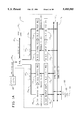
- FIGS. 1A and 2 A general view of the overall system involved is seen in FIGS. 1A and 2 wherein a pair of system busses 12 a and 12 b are each interconnected to a number of resource modules in the system.
- These resource modules include a central processing module 8 in which there resides a bus interface unit 10.
- This bus interface unit actually is a dual unit of which one operates with a system bus A, 12 a and the other unit cooperates with the system bus B, 12 b .
- the additional resources connected to both of the system busses include a memory control module MCM 48 (memory unit) and an input/output module 68 (IOM) which provides communication with various peripherals attached to the system in addition to a task control unit 88 (TCU) which controls the allocation of system tasks, and an external message interface unit 98 (PMIU) which connects to a system having non-compatible protocol operations.
- MCM 48 memory unit
- IOM input/output module 68
- TCU task control unit 88
- PMIU external message interface unit 98
- this disclosure is particularly involved with the function and operation of the bus interface unit 10 having two channels 10 a , 10 b operating in a dual capacity such that the system bus A, 12 a will have its own bus interface channel 10 a (FIG. 1) and also the other system bus B, 12 b will have its own dedicated bus interface channel 10 b (FIG. 1).
- FIG. 1 is a generalized overall view of the dual bus interface unit 10 indicating its major components for integrating communication between dual systems busses and the Translation Logic 20 and Processor 28.
- the M bus 28m connects the bus exchange 15 to the mainframe processor 28 while the T bus 20 t connects the translation logic unit 20 to the bus exchange.
- Channel A, 10 a and Channel B, 10 b respectively use the A bus 15 a and B bus 15 b with a series of state machines 10 ta , 10 tb ; 10 ra , 10 rb ; and 10 rta , 10 rtb .
- the bus interface unit 10 is further shown in FIG. 1A and functions to permit the processor 28 and the translation logic 20 to communicate with the dual bus system, that is to say, system busses 12 a and 12 b .
- the processor 28 is capable of executing Reads or Writes to the system memory 48 of FIG. 1A.
- the mainframe processor 28 can also read the time of day from the input/output module 68 which houses the system clock. Thus there can be enabled, through the bus interface unit 10, a flow of data from either one of the system busses A or B, to and from the mainframe processor 28 and/or the translation logic unit 20.
- FIG. 1B shows data sent to the system busses 12 a , 12 b
- FIG. 1C shows data returned from the system bus to the bus interface unit 10 (BIU) for transfer to the mainframe processor 28.
- FIG. 1B there is indicated the transfer of data and commands from the processor 28 through the memory bus exchange 15 and thence to either the A bus output register 16 a0 or to the B bus output register 16 b0 .
- a and B bus registers respectively connect to the system A bus 12 a and the system B 12 b .
- the processor interface logic in 28 sends a command to the bus interface logic unit 10 (BIU) along with a BIU 10 request signal.
- BIU bus interface logic unit 10
- the command and the address are loaded into the output registers 16 a0 and 16 b0 for conveyance to both system busses.
- the Bus Interface Unit 10 will then make a request to the system bus arbitrators (in the Central Processing Module 8 of FIGS. 2, 4) for use of a system bus.
- the bus interface unit 10 executes all the necessary system bus protocols unique to the system bus 12 in order to send the command, the address (and data if there is required an "overwrite” to the system memory 48). If a "Read” cycle is commanded, then the requested data is returned from the memory 48, checked for parity, and the data is then sent to the central processor 28, FIG. 1A.
- data taken from the memory unit 48 can be transferred on either bus, but, in this case specifically on system bus A, 12 a , over to the A bus input register 18 ai and thence on the A bus 15a to internal register 16 ai from which it is conveyed to the memory bus exchange 15 for subsequent transfer to the processor 28.
- the translation logic 20 serves the function of providing an interface for handling the mainframe processor protocol which uses one 52-bit word and transfers this into 4 word messages for compatibility with an external digital system 98 using a different clock rate and protocol; thus the translation logic 20 of FIGS. 3A and 3B "Writes to" and also receives four word messages from the system busses 12 a and 12 b .
- the data flow is seen in FIG. 3A as the transfer of four words from the translation logic 20 to the memory bus exchange 15 and thence to the A bus and B bus output registers (16 a0 , 16 b0 ) for conveyance to the system A bus 12 a and the system B bus 126.
- the translation logic 20 wants to send a message to the input/output module 68, a request is made to the bus interface unit BIU 10 (FIG. 1A). Once a grant is made by the bus interface unit, BIU 10, the message command word will be loaded into both of the BIU output registers 16 a0 , 16 b0 for both system busses. The BIU 10 (Bus Interface Unit) will then make a request to the system bus arbitrators (in the CPM 8) for use of a system bus such as 12 a or 12 b . When a system bus has been granted, the BIU 10 will execute all necessary system bus protocols which are required by the bus to send the command and also the four data words to the input/output module IOM 68.
- the BIU 10 (Bus Interface Unit) continuously monitors the system busses for messages which are addressed to the central processing module 8 (CPM).
- the system bus is continually loading data into the input registers 18 ai , 18 bi of the BIU 10.
- PENRDY denotes "processing element" not ready.
- the message transfer will pause until the "not ready” signal goes away and then the BIU 10 will then load it into the translation box logic unit 20.
- the BIU 10 may also issue a signal designated A-RETRY-B or B-RETRY-B to the message, if it is currently unable to process the message. Finally, when it can accept the message, and check the parity and send the four data words to the translation logic 20, the BIU 10 will do so. The BIU 10 will execute all necessary system bus protocols unique to the system bus in order to facilitate the message transfer.
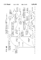
- FIG. 4 is a generalized block diagram showing the relationship of logic units the central processing module 8 which holds, the translator logic 20 and the bus interface unit 10. In addition, FIG. 1, also shows this relationship indicating how the two channels A and B (15 a , 15 b ) are organized.
- the central processing module 8 contains the mainframe processor 28 (IMP) and a number of other generalized functional blocks shown in FIG. 4. Connected to the processor logic of the CPM 8 is the translator logic 20. As shown in FIG. 4, this involves the translator box 20 x , the translator box controller 20 c , and the translator box memory RAM 20 r .
- the logic unit designated as the bus interface unit logic BIU 10 is shown in a generalized block form with blocks indicating the Mix unit 10 m , the Error Logging unit 10 u , the Parity Check Unit 10 pc , and the Timeout Unit 10 tm . Additionally, there are shown the return unit state machine RETURNA designated 10 rta and also the RETURN B unit state machine, 10 rtb . Additionally are shown the bus interface transmit programmable array logic such as 10 ta and 10 tb and the bus interface receive programmable array logic designated 10 ra and 10 rb . Each system bus A and system bus B will connect to a decoder 10 d (10 da and 10 db ) which provides decoding functions for the system busses 12 a and 12 b .
- the Mix Unit, 10m, of FIG. 4 combines control signals from both system busses into one signal for the processor control logic unit in CPM 8. It also functions to stop incoming messages to the CPM 8 from a system bus, if the CPM 8 is not ready to accept the message.
- the Decoder 10 da and 10 da of FIG. 4 functions to monitor the system busses, 12 a and 12 b to notify the BIU 10 that a bus message is designated for the host CPM 8. It also functions to see if a "Write Command" on the system bus should be invalidated in cache memory as being no longer valid data.
- the mainframe processor control logic in the CPM 8, FIG. 4 will receive completion status signals from a system bus when a given command cycle has been completed.
- the multiple bus exchange 15 allows the mainframe processor 28, the translation logic unit 20 and the BIU 10 to exchange data.
- the processor 28 can read or write the transfer unit 20 or read from or write data to the BIU 10.
- Control lines determine which modules are sources and which are receiving units.
- the bus interface unit logic 10 will be seen to have two programmable array logic state machines, one for each channel for each of the system busses. These are designated as transmit (XMT) state machines which provide the functions seen in FIGS. 5A and 5B.
- XMT transmit
- the BIU-XMT programmable array logic is a state machine which may be implemented by use of a Signetics chip PLUS405 running at 16 megahertz. Its main function is to handle the system bus protocols for carrying out the various system bus operations which are initiated by the processor 28 (IMP) or transfer box logic 20. There is one bus interface unit transmit PAL (BIU-XMT) for each system bus.
- FIG. 5A is a block diagram of the bus interface unit transmit programmable array logic unit (BIU-XMT) and the signals which interface with it.
- BIU-XMT programmable array logic unit
- x-RETRY-B refers to two signals, that is to say A-RETRY-B and also B-RETRY-B.
- n is used to indicate a number so that for instance--MSGn represents MSGn. MSG2, and so on. MSG stands for message number.
- FIG. 5A is a drawing illustrating the transmit function of the bus interface unit and its relationship to other modules in the system.
- FIG. 5A shows how various signals from the processor logic 28, the Error Logging unit 10 u and the translator box logic 20 are sent to the bus interface unit programmable transmit logic 10 ta .
- the bus transmit programmable array logic 10 ta receives a series of signals from the A Bus 12 a and also outputs a series of signals to the A Bus 12 a as shown in the drawings of FIG. 5A. Also the transmit unit 10 ta provides signals to the A Bus output register 16 a0 and to the A Bus output buffer 16 a0b .
- the timeout unit 10 tm and the parity check unit 10 pc provide signal lines into the bus interface unit transmit programmable logic 10 ta .
- FIG. 5A basically indicates commands and data transfers from the processor 28 (IMP) or from the transfer box 20 x to the system busses 12 a , 12 b .
- the transfer box messages can be serviced for transfer to the busses 12 a and 12 b .
- a system bus signal will permit commands to be transmitted from the IMP processor 28 or the transfer box 20 x .
- mainframe processor 28 and the translation box logic 20 are capable of sending and receiving messages via a dual system bus architecture which caries message protocols different from the message protocols used by the mainframe processor.
- the attached Table I will illustrate how the mainframe processor 28 provides message commands and how each command is encoded when it is sent to the bus interface unit-transmit programmable array logic 10 ta .
- the state machine will abort the operation and if the retry limit has not been met, will retry the operation at a later time.
- This signal indicates that some active receiver on the system bus has detected a parity error.
- PROCR (IMP) Command (M -- CMD016, M -- CMD116)
- This signal indicates that there is an operation which is active on the system bus.
- This signal validated with x -- BUSBUSY -- B, indicates that the requesting CPM has been granted the indicated system bus for a bus operation.
- This signal is used to determine when a bus operation has timed out. This can occur while waiting for a system bus grant after a system bus request, waiting for a not ready signal to go inactive while executing a bus operation, or waiting for data to be returned while executing a read type operation.
- This signal becomes active when the TBOX wishes to send a message to a system bus.
- This signal is asserted whenever a parity error is detected on one of the system buses.
- This signal is a test bit used during board debug. It causes the BIU-XMT PAL to assert the signals B -- DRIVE -- B and x -- BBSY -- B.
- This signal is asserted by the PMIU 98 when it has successfully accepted a message from the CPM or is acknowledging that it has received a read time of day, RTOD command.
- Source Sx -- MMACK -- B buffered by Receiver.
- This signal is asserted by memory to acknowledge that it has received a valid command.
- This signal validates the IMP Command bits.
- the BIU-XMT PAL is executing a system bus operation and this signal is asserted by the receiving module, the operation will be aborted and, if the retry limit has not been exceeded, the operation will be retried at a later time.
- This signal indicates that some active receiver on the system bus has detected a parity error.
- This signal indicates that the current bus operation has completed successfully.
- BIU-XMT States There are twenty operative states associated with this BIU-XMT state machine. It is to be noted that the bus interface unit transmit programmable array logic, 10ta will operate as a state machine. This is indicated in FIG. 5B which shows the various routines which can be provided by the bus interface transmit unit 10 ta . Similarly this set of routines is also provided by the second bus interface transmit programmable array logic 10 tb which performs the same set of automatic functions shown in FIG. 5B.
- FIG. 6A shows a drawing of the bus interface unit programmable array logic state machine designated 10ra.
- the BIU-RCV programmable array logic is a state machine which is implemented, for example, by means of a Signetics PLUS405 type of device running at 16 megahertz. Its chief function is to control and handle messages coming in on one of the system busses (12.sub., 12 b ) which is addressed for a particular central processing module CPM.
- the bus interface unit-receive state machine 10 ra is the central programmable array logic unit of FIG. 6A which is shown having a set of signal line connections to certain elements of the system. It should be noted that the programmable array logic will assert to the system certain signals such as bus retries, bus errors and not-ready signals as appropriate. In the described system there is one bus interface receive state machine for each of the system busses 12 a and 12 b .
- the bus interface unit-receive state machine will interchange signals with the system bus 12 a and also with the A Bus internal register 16 ai in addition to the cache unit 40 c and the translation box logic unit 20 x , FIG. 3A.
- Other input lines to the bus interface unit-receive state machine are seen to be supplied by the Mix unit 10 m , the parity check unit 10 pc , the timeout unit 10 tm , the return unit 10 rta and the decoder 10 d .
- the BIU-RCV state machine is a dual bus receiving and routing system for receiving non-compatible protocol messages for storage in TBOX 20 x and translation for message protocol compatibility to the Central Processing Module CPM 8. It controls and handles messages coming in on system busses 12 a , 12 b which are addressed to a particular CPM processor (if more than one CPM is used) or addressed to a translation box logic unit 20 in the CPM 8, FIG. 4.
- the BIU-RCV will also assert the signal Sx -- BERR -- B if a parity error is detected; or it can assert Sx -- RETRY -- B if a message should be retried at a later time; or it can assert Sx -- NRDY -- B if a message needs to be held a few clocks before it can be accepted.
- the BIU-RCV PAL detects a parity error on the system bus and is asserting x -- Bus error -- B, or the BIU-RCV is asserting x -- RETRY -- B, it will continue to assert these signals for two clocks after x -- PENRDY -- B has become inactive.
- This signal indicates to the BIU-RCV PAL that a message for the host CPM 8 has been detected on the system bus (12 a , 12 b ).
- the BIU-RCV PAL will assert x -- RETRY -- B.
- This signal is active during the data phase of system bus operations. It is a registered input to the CPM card.
- This signal indicates that some active receiver on the system bus has detected a parity error.
- the cache asserts this signal when its invalidation queue has filled or otherwise cannot proceed with invalidations. It causes the BIU-RCV PAL to assert a retry when a write operation initiated by a another processing element is detected on the system bus.
- This signal is asserted whenever a parity error is detected on one of the system buses.
- the TBOX asserts this signal whenever it is unable to process any new incoming messages from the system bus or is unable to service a request from the processor 28 IMP.
- the BIU-RCV detects a parity error on the system bus and is asserting x -- Bus error -- B, or the BIU-RCV PAL is asserting x -- RETRY -- B, it will continue to assert these signals for two clocks after x -- MMNRDY -- B has become inactive.
- This signal indicates that a bus requestor has control of the system bus.
- This signal indicates that the BIU-XMT PAL is currently executing a bus operation.
- This signal from the opposite BIU-RCV PAL indicates that it is asserting "not ready” on its system bus. This is used to detect and escape a possible dead lock condition.
- the bus interface unit receive state machine also has a number of output lines which are listed below together with their functions:
- This signal is the x -- INVCMD signal delayed for one clock.
- this signal is asserted on to the system bus to the message originator, to indicate the message has been correctly received.
- this signal loads the internal register as valid data is being received in the input register.
- This signal will be asserted for messages if the TBOX 20 is busy doing another operation or if simultaneous messages are received on both buses. It will also be asserted for write type system bus operations if the cache is currently unable to service the invalidation.
- This signal is asserted as Sx -- PENRDY -- B on the system bus after traveling through an inverting open collector buffer. It is asserted when a message is loaded into the input register while BIU -- NRDY -- B is active.
- the state machine functions provided by the bus interface unit-receive state machine involve some eleven automatic functions which are shown in FIG. 6B.
- bus interface unit-receive state machine The following list indicates the operations provided by the various functions of the bus interface unit-receive state machine:
- FIG. 7A is a block diagram showing the signals which relate to the RETURN A state machine 10rta.
- This state machine has the function to control the select lines of the multiple bus exchange 15 and to signal the mainframe processor logic 28 when "read" data is being returned to it or when an operation has been completed. It will also signal if there was an error that prevented the operation from being completed successfully.
- RETURN A 10 rta
- RETURN B 10 rtb
- the only difference between the two programmable array logic units is the encoding on the select lines to the multiple bus exchange 15 of the two busses.
- RETURN x will refer to the features of both of these programmable array logic units.
- the Return PAL is a state machine implemented with a Signetics PLUS 405 device operating at 16 MHZ.
- the RETURN programmable array logic 10 rta will be seen to receive signals from the parity check unit 10 pc , from the bus interface transmit unit 10 ta , from the error log bus interface 10 u , from the mainframe processor logic 28, from the translator box unit 20 x , and from the bus interface receive unit 10 ra and the timeout unit 10 tm . Additionally, there is an input line from the system bus such as 12 a to the return logic 10 rta .
- the RETURN programmable array logic 10 rta will be seen to provide output signals to the multi-bus exchange 15, to the processor logic 28, to the MIX unit 10 m and to the A Bus internal register 18 ai .
- the Return-PAL provides a dual bus signal control operation for a processor. It allows "read data" from a dual system bus to be sent to the mainframe processor 28 and signals whether the read command was completed successfully or unsuccessfully. It detects and decides whether the operation should be re-tried or not and tells the mainframe processor the final result status. This is accomplished for each bus of the dual system busses.
- FIG. 7A INPUTS TO RETURN PAL
- This signal becomes active when a system bus operation has completed successfully.
- This signal indicates that the bus operation in progress had an invalid address error. This means that the destination module did not provide an acknowledge when a operation was directed towards it.
- this signal becomes active, it indicates that the bus operation in progress had to be aborted. This could be because of a parity error on the system bus, a timeout, or a module asserting retry during an operation.
- This signal indicates the "data phase” during the current bus operation.
- This signal indicates the command phase during the current bus operation.
- PROCR (IMP) BIU Request (M -- BREQ16 -- B)
- This signal validates the mainframe processor IMP Command bits.
- This signal indicates that the mainframe processor (IMP) has received an invalid address error and is now reading the address out of the internal registers, 18 ai , 18 bi .
- This signal indicates to the BIU 10 that the TBOX 20 would like to start sending a message onto a system bus.
- this signal becomes active, it indicates that the present operation has timed out waiting for a system bus grant or waiting for data to be returned during a read type operation.
- This signal is active during the data phase of system bus operations. It is a registered input to the CPM 8 card.
- This signal will be active whenever the BIU-RCV PAL is in the process of receiving a message from the system bus.
- This signal is asserted whenever a parity error is detected on one of the system buses.
- This test signal causes the internal registers 18 ai , 18 bi to drive their data and the multiple bus exchange 15 to source the A or B bus.
- the RETURN programmable array logic unit-state machine, 10rta of FIG. 7A has a number of output lines which are listed hereinbelow in addition to Table II which indicates the RETURN select lines:
- This signal being active causes the internal registers (18 ai , 18 bi ) to load data on the RxBUS.
- this signal When this signal is returned from the BIU logic it indicates that an operation finished with an error such as a parity error, a retry limit, or an invalid address.
- This signal indicates which system bus an operation went out on. It is used to let the mainframe processor (IMP) logic know which bus to access when read data is returned.
- IMP mainframe processor
- This signal causes the internal register (18 ai , 18 bi ) to drive its contents onto the A or B bus.
- This signal indicates to the processor (IMP) logic that valid read data is being driven to the M -- BUS, 28 m .
- this signal will be driven to the IMP Logic.
- FIG. 7B shows the various functions provided by the RETURN PAL state machine which is resident in the hardware of FIG. 7A. As seen in FIG. 7B, there are 14 functional operational states associated with the RETURN state machine 10 rta or 10 rtb .
- the timeout state machine is a programmable array logic unit which is state machine implemented, usually by means of a Signetics PLUS405 device, which runs at 16 Megahertz.
- the chief function of the timeout state machine is to send out a request for use of the system bus (12a, 12b) and also to determine if an operation has already timed out.
- timeout state machine 10 tn is connected to various of the other modules in the bus interface unit system.
- the timeout state machine 10 tm will be seen to receive signals from the system bus such as 12 a , 12b, from the bus interface unit receive logic state machine 10 ra , from the error log unit 10 u , from the processor logic 28, from the translator box 20 x , from the mix unit 20 m , from the second bus interface unit receive state machine B, 10 rb .
- timeout state machine will provide certain output signals as seen in FIG. 8A to the bus 12 a or 12 b , to the A Bus output register 18 a0 , to the return array logic 10 rta , to the bus interface unit transmit state machine 10 ta , 10 tb , to the bus interface unit receive state machine 10 ra , to the processor logic 28 and, to the MIX unit 20 m and also to the transmit and receive state machines 10 ta , 10 tb , 10 ra , 10 rb , and the RETURN programmable array logic 10 rtb , and 10 rta .
- FIG. 8A shows the timeout state machine 10 tm and the related modules with which it operates. This could be described as a system for requesting bus access (system bus A and B) and setting time limitations for execution of command cycles.
- the timeout state machine FIG. 8B does several important things, for example it checks to see if a command operation has "timed out", and is considered as an "error". This indicates that the time allotted for a given operation has exceeded 512 microseconds. The system will allow up to 16 tries for this type error or other errors.
- timeout state machine also functions to put out a bus request to access a system bus.
- a number of input signals are provided to the timeout state machine 10 tm .
- the first group of inputs come from the system busses such as system bus A and system bus B. These signals include the system bus A grant and the system bus B grant. Once the timeout state machine has made a system bus request, this signal (validated with A bus busy or B bus busy) will indicate that the operation has been granted access to system bus, which ever bus is not busy A or system bus B.
- the other inputs to the timeout state machine from the system bus include the system bus A-busy and the system bus B-busy signals. These signals will indicate that a bus operation is already currently in progress on system bus A or system bus B.
- the other input from the system bus to the timeout state machine is the clock signal designated as the 512 microsecond clock signal. This clock signal is to determine when bus access operations have timed out because each bus is busy or not available for too long a period.
- the error logging bus interface unit 10 u There are a series of inputs from the error logging bus interface unit 10 u which signals include the processor bus interface unit request signal, and the Read invalid address signal which indicates that the processor has received an invalid address error and is now reading the address out of the internal registers.
- the processor bus interface unit request signal is a signal which validates the command signals for the processor 28.
- Added further inputs from the error log unit 10 u , to the timeout state machine 10 tm include the TBOX retry signal which causes the transfer box 20 x to stop sending a message and to retry again once the signal is inactive. It causes the timeout state machine 10 tm to remain in the idle state while it is active.
- the final signal from the error unit 10 u is the processor retry signal. If this signal becomes active, it causes the processor logic 28 to stop sending its commands to the bus interface unit 10 and to retry it again once the signal is inactive. It causes the timeout state machine to remain in the idle state while the signal is active
- processor command signals contain encoded values which were shown in Table I.
- the transfer box 20 x provides an input signal to the timeout state machine 10 tm which is designated as the transfer box bus interface unit request signal. This signal indicates to the bus interface unit 10 that the transfer box would like to start sending a message onto the system bus (12 a , 12 b ).
- the mix logic 20 m of FIG. 8A provides an output signal to the timeout state machine which is designated as the bus interface unit data acknowledge signal. This signal indicates to the receiver that the current operation is completed, and the data is being returned from the system bus to the processor 28, and is now valid.
- the bus interface receive state machines 10 ra and 10 rb each provide inputs to the timeout state machine. These are called the A side receiving message and the B side receiving messages so that this signal will be active whenever the receiving state machine is in the process of receiving a message from the A system bus 12 a or alternatively from the B system bus 12 b .
- Another input is provided to the timeout state machine 10 tm by a signal line from the MIX unit 20 m .
- This signal is the bus interface unit data acknowledge signal. This signal indicates to the timeout 10 tm state machine that the current operation has been completed and if data is being returned from the system bus (12 a , 12 b ) to the processor 28, this data is now valid.
- the timeout state machine 10 tm provides a series of output signals to the related modules in the system as discussed hereinunder.
- the bus interface unit processor grant signal is seen provided as an output from the timeout state machine to the processor 28. This signal indicates to the IMP processor logic that the bus interface unit 10 has accepted and loaded the command and the address and is now ready to accept the data during an operation.
- timeout state machine There are two outputs from the timeout state machine which are fed to the bus interface unit receive state machines A and B (10 ra , 10 rb ) by means of signals designated as the bus interface unit-not ready signal. This signal tells the BIU receive-state machine that any incoming message should get a "not ready”. The timeout state machine issues this command when it will be finishing an operation in a few clocks and when it is safe to write over the internal registers, 16 ai , 16 bi .
- timeout state machine 10 tm There are two outputs from the timeout state machine 10 tm to each of the A and B transmit state machines 10 ta and 10 tb . These signals are designated as the operation timeout signal. If this signal becomes active it indicates that the present operation has timed out waiting for a system bus grant or waiting for data to be returned during a read operation, or a destination module has asserted itself as not being ready for too long a period. It will be noted that this operation timeout signal is also conveyed to the return state machines 10 rta and 10 rtb .
- the timeout state machine 10 tm puts an output signal to the A and B bus output register 18 a0 , 18 ab , which is known as the load output register signal. This signal causes the output registers for the A bus and the B bus to load data.
- the final output line of the timeout state machine 10 tm is a signal line to the system busses (12 a , 12 b ,) and provides a signal designated as the system bus request signal.
- This signal causes a request to a system bus arbitrator in the central processing module 8 for use of one of the system busses. It will remain active until a bus is granted or else the request is timed out.
- FIG. 8B is a flow chart diagram which shows the functional operations of the timeout state machine. As seen in FIG. 8B the basic function in the timeout machine is to note that when a request for data is made, then there is a waiting or a busy period available for subsequent requests until the timeout period has occurred at which case the command cycle will come to a stop.
- the situation for a Write operation shows that after a bus grant and a Write wait period, then the condition will revert to the timeout period which will result in a stop indicating that none of the resources were available to allow the command cycle to be completed.
- this signal validated with A -- BUSBUSY -- B, will indicate that the operation has been granted system bus A.
- this signal validated with B -- BUSBUSY -- B, will indicate that the operation has been granted system bus B.
- This signal indicates that a bus operation is currently in progress on system bus A.
- This signal indicates that a bus operation is currently in progress on system bus B.
- This signal indicates to the receiver that the current operation has been completed and if data is being returned from the system bus to the processor logic, it is now valid.
- This signal indicates to the BIU 10 that the TBOX 20 would like to start sending a message onto the system bus.
- Source CMDREQ PAL synchronized in Error Log Unit.
- This signal validates the signals M -- CMD016 and M -- CMD116.
- This 512 microsecond clock is used to determine when bus operations have timed out.
- This signal indicates that the IMP processor has received an invalid address error and is now reading the address out of the internal registers.
- This signal indicates that valid data is being driven to the BIU logic by the IMP processor 28.
- This signal will be active whenever the BIU-RCV PAL is in the process of receiving a message from the A side system bus.
- This signal will be active whenever the BIU-RCV PAL is in the process of receiving a message from the B side system bus.
- this signal becomes active, it causes the TBOX 20 to stop sending a message and to retry again once the signal is inactive. It causes the TIMEOUT PAL to remain in the idle state while it is active.
- this signal becomes active, it causes the IMP processor logic to stop sending its operation to the BIU 10 and to retry again once the signal is inactive. It causes the TIMEOUT PAL to remain in the idle state while it is active.
- the Timeout state machine also includes a number of output signal lines which are listed hereinbelow together with their function:
- This signal makes a request to the system bus arbitrator for use of one of the system buses. It will remain active until a bus is granted or it is timed out.
- this signal becomes active, it indicates that the present operation has timed out waiting for a system bus grant, or waiting for data to be returned during a read type operation, or a destination module has asserted not-ready too long.
- This signal causes the output registers (16 ao , 16 bo ) for the A and B bus to load data.
- This signal indicates to the IMP processor logic that the BIU 10 has accepted and loaded the command and address, and is now ready to accept the data during an operation.
- This signal tells the BIU-RCV PAL that any incoming message should get a retry.
- the TIMEOUT PAL issues this command to prevent the internal registers from being overwritten.
- This signal tells the BIU-RCV PAL that any incoming message should get a not-ready.
- the TIMEOUT PAL issues this command when it will be finishing an operation in a few clocks and it is safe to write over the internal registers, 16 ai , 16 bi .
- the timeout state machine provides some twelve discrete functional states which are shown in FIG. 8B. The various states and the state transitions involved are listed hereinbelow together with the functions that they provide.
- Described herein has been a programmable timing logic system for allocating limited and predetermined time usage of two system busses for data transfers between a central processor and/or protocol translation unit (TBOX) and data on dual system busses which move to/from external digital modules connected to the system busses. Incomplete cycles are error logged and given a specified number of retries during a limited pre-set time period, after which the allocation of system bus usage is granted to other requesting units on a time limited basis.
- TBOX protocol translation unit
- the bus interface unit integrates data transfer operations between a first computer system, operating under a first message protocol and first clock speed, with a second digital system operating under a second message protocol type and second clock speed.
Landscapes
- Engineering & Computer Science (AREA)
- Theoretical Computer Science (AREA)
- General Engineering & Computer Science (AREA)
- Physics & Mathematics (AREA)
- General Physics & Mathematics (AREA)
- Computer Hardware Design (AREA)
- Bus Control (AREA)
Abstract
Description
              TABLE I
______________________________________
COMMAND ENCODINGS
PROC IMP Operation
             M CMD (1:0) (M Bus 28 m, FIG. 1
______________________________________
Read         00
Read Next Code
             00
Readcode     00
Fetchcode    00
Read TOD     01
Overwrite    10
Send Message 10
Readlock     11
______________________________________
______________________________________
IDLE   When the reset signal (405-RESET X) is applied to
       the BIU-RCV PAL, the internal state machine will
       go to the IDLE state. While in this state, all
       output signals are inactive.
CMD    This indicates the command phase of a bus
       operation. In this state the active outputs are
       .sub.x- BBSY.sub.- B, which indicates a valid operation is
       occurring on the system bus, B.sub.x- DRIVE.sub.- B, which
       output enables the output registers to the system
       bus; .sub.x- CMDVLD.sub.- B, which indicates that a valid bus
       command is on the system bus; and .sub.x- LDOREG.sub.- B,
       which loads the output registers with the data
       for the data phase of an operation.
MSGn   (For values of n equal to 1, 2, or 3) During
       these states the data words of a message are
       being sent out on the system bus. The active
       outputs are .sub.x- BBSY.sub.- B indicating the system bus is
       busy; B.sub.x- DRIVE.sub.- B, output enabling the output
       drivers; .sub.x- LDOREG.sub.- B, which loads the next data
       word to be sent out in the message; and
       .sub.x- DATVLD.sub.- B, which indicates there is valid data
       on the system bus.
MSG4   This state is similar to the above message states
       except .sub.x- LDOREG.sub.- B is no longer active.
CHPS   This is a one clock state waiting to look for
       .sub.x- PEACK.sub.- B from the message destination module.
       There are no active outputs. PEACK denotes
       Processing Element Acknowledgement.
CHPA   The state machine is looking for the xPEACK.sub.- B
       from the destination module during this state.
       There are no active outputs.
DAT1   This is the data phase state during overwrite and
       readlock operations. The active outputs are
       .sub.x- BBSY.sub.- B, B.sub.x- DRIVE.sub.- B, and
       .sub.x- DATVLD.sub.- B.
WAIT   During a read operation the state machine will
       pause here until .sub.x- MMNRDY.sub.- B and .sub.x- PENRDY.sub.- B
       are
       both inactive. The only active output is
       .sub.x- BBSY.sub.- B.
WAIT2  During a readlock operation the state machine
       will pause here one clock before looking for an
       acknowledge signal from the destination module.
       The only active output is xBBSY.sub.- B.
CHKS   During an overwrite operation the state machine
       will pause here one clock before looking for an
       acknowledge signal from the destination module.
       The only active output is .sub.x- BBSY.sub.- B.
CHKA   At this point in a read or a readlock operation
       the state machine is looking for the signal
       .sub.x- MMACK.sub.- B or .sub.x- PEACK.sub.- B from the
       destination
       module. The only active output is .sub.x- BBSY.sub.- B.
CHKO   At this point in an overwrite operation the state
       machine is looking for the signal .sub.x- MMACK.sub.- B from
       the destination module. The only active output
       is .sub.x- BBSY.sub.- B.
READ   The state machine will pause in this state during
       a read or readlock operation waiting for valid
       data to come back from the destination module.
       The only active output is x.sub.- BBSY.sub.- B.
RDDK   If valid data has been returned from the
       destination module, indicated by entering this
       state, the active outputs will be .sub.x- BBSY.sub.- B and
       .sub.x- DACK.sub.- B. It will then return to IDLE state.
DACK   If an overwrite or message operation has
       completed successfully, this state will assert
       .sub.x- DACK.sub.- B.
INVA   This state indicates that no valid acknowledge
       has been received from a destination module
       during a bus operation. The outputs are .sub.x- BBSY.sub.- B
       and .sub.x- INVADR.sub.- B. .sub.x- BBSY.sub.- B is asserted to
       protect
       the invalid address stored in the internal
       registers, as 16.sub.bi.
BERR   This state indicates that an error has occurred
       during a bus operation, such as a timeout or a
       parity error. It could also enter this state
       because another module on the system bus has
       asserted a retry. The only active output is
       .sub.x- ABORT.sub.- B.
TEST   This state is used during board test. When in
       this state the outputs are .sub.x- BBSY.sub.- B and
       B.sub.x- DRIVE.sub.- B.
______________________________________
______________________________________
State Transitions of BIU-XMT (FIG. 5B):
______________________________________
IDLE to If the system bus grant signal S.sub.x- BGNT.sub.x- B
CMD:    becomes active while .sub.x- BBSY.sub.- B and TIMEOUT.sub.- B
        are inactive, this indicates that the
        BIU-XMT state machine has been granted the
        system bus and can proceed to carry out a
        bus operation.
CMD to  If the TBOX 20 is the requestor to the
MSG1:   BIU 10 and TIMEOUT.sub.- B is not active, the
        transmit state machine will proceed to send
        the first data word of the message onto the
        system bus , 12.sub.a, 12.sub.b.
MSGn to If each of the four words of a TBOX
MSGn+1: message are sent correctly without any
        errors such as parity errors, timeouts,
        or retries, the transmit state machine
        will transition to the next state each
        clock. If .sub.x- PENRDY.sub.- B becomes active
        during any of these states, it will
        stay in that state until xPENRDY.sub.- B
        becomes inactive, transitioning to the
        next message state, or an error or a
        retry occurs which causes a transition
        to BERR.
MSG4    If the fourth data word of a message has
to CHPS:
        been sent correctly with no errors or
        retries, this transition will occur.
CHPS    If no errors occurred during CHPS state,
to CHPA:
        this transition will occur.
CHPS    If a bus error, retry, or timeout occurs,
to BERR:
        this transition will occur.
CHPA    If .sub.x- PEACK.sub.- B becomes active while in this
to DACK:
        state, indicating that the destination
        module has correctly received the message,
        this transition will occur indicating to the
        CPM logic 8 that the message has been sent
        correctly.
CHPA    If .sub.x- PEACK.sub.- B is not active during CHPA,
to INVA:
        indicating that the destination module did
        not correctly receive the message, this
        transition will occur indicating to the CPM
        logic 8 that the message had an invalid
        address error.
IDLE    If TS.sub.- XBDRV.sub.- B is active during a board test
to TEST:
        operation, this transition will occur.
CMD     During a read operation, if a timeout has
to WAIT:
        not occurred, this transition will be made.
        This is a transition to the data phase of a
        read operation. The state machine will stay
        in the WAIT state while either .sub.x- MMNRDY.sub.- B or
        .sub.x- PENRDY.sub.- B are active.
WAIT    If TIMEOUT.sub.- B becomes active, an error has
to BERR:
        occurred and this transition will be made.
WAIT    During a read operation, if the destination
to CHKA:
        module is ready and no timeout has occurred,
        this transition will be made.
CHKA    If the destination module has acknowledged
to READ:
        the bus operation by asserting either
        .sub.x- PEACK.sub.- B or .sub.x- MMACK.sub.- B, and a bus error
        or a
        retry do not occur, this transition will be
        made.
CHKA    This transition will be made if the
to INVA:
        destination module does not acknowledge the
        operation during this clock and a bus error
        or a retry do not occur.
CHKA    If a bus error or a retry occur during this
to BERR:
        clock, this transition will take place.
READ    The state machine will idle in this state
to RDDK:
        until .sub.x- DATVLDFF.sub.- B becomes active or until a
        parity error or a timeout occurs. When
        valid data has been received, this
        transition will occur.
READ    If a parity error or a timeout occur while
to BERR:
        waiting for valid data, this transition will
        signal these events.
RDDK    RDDK is a one clock state asserting .sub.x- DACK.sub.- B
to IDLE:
        to the rest of the CPM logic 8 indicating
        the read data has been received
        successfully.
CMD     For an overwrite or a readlock operation,
to DAT1:
        this is the transition to the data phase
        when there has been no timeout.
DAT1    If a timeout occurs while waiting for
to BERR:
        .sub.x- MMNRDY.sub.- B to become not active, this
        transition will take place.
DAT1    During a readlock operation, when .sub.x- MMNRDY.sub.- B
to WAIT2:
        becomes not active and no timeout occurs,
        this transition will take place.
DAT1    During an overwrite operation, when
to CHKS:
        x.sub.- MMNRDY.sub.- B becomes not active and no timeout
        occurs, this transition will take place.
WAIT2   This is a one clock wait state during a
to CHKA:
        readlock operation pausing until the next
        clock so acknowledgement can be checked.
        This transition will only occur if no bus
        error or retry signal becomes active.
WAIT2   If a bus error or retry signal becomes
to BERR:
        active, this transition will take place.
CHKS    If a bus error or retry signal becomes
to BERR:
        active, this transition will take place.
CHKS    If no bus error or retry signal becomes
to CHKO:
        active, this transition will take place.
CHKO    This is a one clock check state to look for
to DACK:
        an .sub.x- MMACK.sub.- B signal from memory on an
        overwrite command. If an acknowledge is
        made and no bus error's or retries are
        active, this transition will occur.
CHKS    If no acknowledge is received from memory,
to INVA:
        which indicates an invalid address, and no
        bus error or retry occurs, this transition
        will occur.
CHKS    If a bus error or retry signal becomes
to BERR:
        active, this transition will take place.
______________________________________
______________________________________
CFULLBFF This flip-flop is used to synchronize the 12Mhz
signal .sub.x- CACHEFULL.sub.- B to 16Mhz.
NRDYBFF  This flip-flop internally extends the "not ready"
         signals .sub.x- MMNRDY.sub.- B and .sub.x- PENRDY.sub.- B so
         the
         signal .sub.x- Bus error O will remain valid for two
         clocks after the "not ready" signals are no longer
         active. It is set when either signal is active
         and reset once both are inactive.
DELAYB   This flip-flop is used to delay the signal
         .sub.x- INVCMD one clock before it is sent to the cache
         invalidation logic.
______________________________________
______________________________________
IDLE   When the reset signal (405.sub.- RESETx) is applied to
       the BIU-RCV PAL, the internal state machine will
       go to the IDLE state (FIG. 6B). It will also
       return to this state after an operation is
       completed. While in this state, all output
       signals are inactive.
MSGn   In this state the active outputs are .sub.x- LDNREG1.sub.- B
       which loads message words into the internal
       register 16.sub.ai from the indicated system bus, and
       .sub.x- RCVG.sub.- B, which indicates that a valid message
       is currently being loaded from the system bus.
BERR   This state asserts the output .sub.x- BERRO. The
       current system bus requestor will see that a
       parity error has been detected and will take
       appropriate action.
RETRY  This state asserts the output .sub.x- RETRYO. This
       will cause the current system bus requestor to
       discontinue the operation and retry at a later
       time.
NRDY1  The current system bus requestor will wait in the
       data phase of the message while .sub.x- NRDYO is active
       in this state. The signals .sub.x- LDNREG1.sub.- B and
       xRCVG.sub.- B will also be asserted.
NRDY2  This state is the same as NRDY1 except that
       .sub.x- LDNREG1.sub.- B is not active because the first
       message word has already been loaded into the
       internal register, 16.sub.ai.
PAUSE  .sub.x- RCVG.sub.- B is asserted in this state while waiting
       for the message to resume being sent.
PEACK  When an entire valid message has been loaded
       from the system bus, this state will assert
       .sub.x- PEACKO.sub.- B. This indicates to the message
       originator that the message has been received
       correctly.
______________________________________
______________________________________
STATE TRANSITIONS: BIU-RCV, FIG. 6B:
______________________________________
IDLE to BERR:
            This transition will occur when a parity
            error has been detected on the system bus
            during the command phase of any bus
            operation and during the data phase of any
            operation in which the host CPM 8 is
            involved.
IDLE to RETRY:
            If a valid message for the host CPM 8 is
            detected on the system bus and the CPM is
            not able to accept it due to the TBOX 20
            being busy, or the cache spy register 40.sub.c
            being full with the cache unable to
            invalidate a system bus write type
            operation, this transition will occur. It
            will also occur in the system bus B BIU-
            RCV PAL if a message is simultaneously
            detected on both the A and B system buses
            at the same time.
IDLE to NRDY1:
            If a valid message for the host CPM 8 is
            detected while the TIMEOUT PAL is
            asserting BIU.sub.- NRDY.sub.- B, this transition will
            occur. This indicates that the BIU 10 is
            currently unable to accept the message but
            will soon be able to.
IDLE to MSG1:
            This transition will occur when an incoming
            message is detected and it would not
            otherwise go to the berr, retry, or nrdy1
            states. This transition will occur if
            .sub.x- MSG.sub.- B is active while none of the
            following are active: xDATAPE.sub.- B,
            BIU.sub.- NRDY.sub.- B, T.sub.- BUSY.sub.- B,
            .sub.x- STOPMSG.sub.- B, other side.sub.- NRDYO, and
            for the B bus BIU-RCV PAL, A.sub.- MSG.sub.- B.
BERR TO IDLE:
            The state machine will stay in the BERR
            state until two clocks after the not ready
            signals .sub.x- PENRDY.sub.- B and .sub.x- MMNRDY.sub.- B
            are no longer active. This is done by having
            the not ready signals set the internal flip-
            flop NRDYBFF and by transitioning, once
            all three signals are inactive.
RETRY to IDLE:
            The receive state machine will stay in the
            RETRY state until two clocks after the "not
            ready" signals .sub.x- PENRDY.sub.- B and
            .sub.x- MMNRDY.sub.- B are no longer active. This
            is done by having the "not ready" signals set
            the internal flip-flop NRDYBFF and by
            transitioning, once all three signals are
            inactive.
MSGn to BERR:
            If a parity error is detected on the system
            bus while a message is being loaded during
            any of these states, this transition will
            occur.
MSGn to IDLE:
            If the signal .sub.x- BBSYFF.sub.- B goes inactive
            while in any of these states, the message
            originator did not complete sending a valid
            message and the state machine will go back
            to idle.
PEACK to IDLE:
            This is an immediate transition once the
            PEACK state has been entered. The
            message has been correctly received and the
            BIU-RCV state machine is going back to
            idle.
NRDY1 to IDLE:
            If the signal .sub.x- Berr.sub.- B is detected on the
            system bus, an error has occurred while
            .sub.x- PENRDY.sub.- B is being asserted. The
            message originator will withdraw from the
            system bus and the state machine will go
            back to idle. If .sub.x- BBSYFF.sub.- B is no longer
            asserted, this indicates the message origina-
            tor has disconnected from the system bus
            and will not complete sending the message.
NRDY1 to    This transition is used to escape from
RETRY:      the "deadlock case" where the CPM 8 has
            sent a message out on one bus, which
            has received an S.sub.x- PENRDY.sub.- B from the
            destination module, while it is
            receiving a message on the other bus
            for which it is asserting its own
            S.sub.x- PENRDY.sub.- B. The signal
            .sub.x- STOPMSG.sub.- B has the signal
            TBXMSG.sub.- OUT or'ed into it which indi-
            cates that the host CPM 8 is sending out a
            message. If the signals .sub.x- STOPMSG.sub.- B and
            T.sub.- BUSY.sub.- B are active, and the BIU-RCV
            PAL is in the NRDY1 state, it knows that a
            deadlock condition has occurred. To escape
            from this, the BIU-RCV asserts a
            .sub.x- RETRYO to the message sending module,
            which will release the two modules from the
            deadlock.
NRDY1 to BERR:
            If the signal .sub.x- DATAPE.sub.- B is active
            during the NRDY1 state indicating a
            parity error on the bus, the BIU-RCV
            PAL will assert .sub.x- Bus error O.
NRDY1 to NRDY2:
            If the signal BIU.sub.- NRDY.sub.- B continues to
            be asserted, no deadlock condition is
            detected, and there are no parity
            errors detected, this transition will
            occur. This transition is necessary so
            the signal .sub.x- LDNREG1.sub.- B is not
            continuously active while .sub.x- NRDYO is
            being asserted.
NRDY1 to PAUSE:
            This transition is made if the signal
            BIU.sub.- NRDY.sub.- B is no longer active while in
            the NRDY1 state. If no deadlock
            condition is detected and there are no
            parity errors detected, this transition
            will occur. This state is necessary to
            wait for the module sending the message
            to see that S.sub.x- PENRDY.sub.- B is no longer
            being asserted and it can now continue
            sending the message.
NRDY2 to BERR:
            If a parity error is detected during this
            state, the BIU-RCV PAL must assert
            .sub.x- Berro and the message will no longer be
            accepted.
NRDY2 to IDLE:
            If the signal .sub.- Buserr.sub.- B is detected from the
            system bus, an error has occurred while
            PENRDY.sub.- B is being asserted. The message
            originator will withdraw from the system
            bus and the state machine will go back to
            idle. If .sub.x- BBSYFF.sub.- B is no longer asserted,
            this indicates the message originator has
            disconnected from the system bus and will
            not complete sending the message.
PAUSE to IDLE:
            If the signal .sub.x-Buserr.sub.- B is detected from
            the system bus, a system bus module has
            detected a parity error. The message
            originator will withdraw from the system
            bus and the state machine will go back to
            idle. If xBBSYFF.sub.- B is no longer asserted,
            this indicates the message originator has
            disconnected from the system bus and will
            not complete sending the message.
PAUSE to BERR:
            If a parity error is detected during this
            state, the BIU.sub.- RCV PAL must assert
            .sub.x- Buserro and the message will no longer
            be accepted.
PAUSE to MSG2:
            If there is no parity error and the message
            originator is still asserting .sub.x- BBSYFF.sub.- B,
            then the rest of the message can now be
            accepted normally.
______________________________________
TABLE II ______________________________________ A SELECT(1:0)A Port Status ______________________________________ 00 M.sub.- BUS drives A.sub.-BUS 01 T.sub.- BUS drives A.sub.-BUS 10 B.sub.- BUS drives A.sub.-BUS 11 Source ______________________________________ B SELECT(1:0)B Port Status ______________________________________ 00 M.sub.- BUS drives B.sub.-BUS 01 T.sub.- BUS drives B.sub.-BUS 10Source 11 A.sub.- BUS drives B.sub.- BUS ______________________________________
______________________________________
RETURN.sub.x :
        Internal Flip-Flop's
INVFF   This internal flip-flop is set when an invalid
        address occurs on the system bus for which each
        particular RETURN PAL is associated. It is used
        so the appropriate sides internal register (18.sub.ai,
        18.sub.bi) is driven when the read invalid address
        command is issued. It is reset when the read
        invalid address command is issued or if any other
        bus command is issued by the processor 28 (IMP).
WAIT    This internal flip-flop is used to assure that
        the invff does not reset during the same
        processor (IMP) operation it is set.
______________________________________
______________________________________
STATES FOR RETURN-PAL:
______________________________________
IDLE     When the reset signal (405.sub.- RESETx) is applied to
         the RETURN.sub.x PAL, the state machine will go to
         the IDLE state FIG. 7B. While in this state, all
         output signals are inactive.
TBOX     This state is entered when the TBOX 20 is attempt-
         ing to send a message out onto the system bus. Its
         purpose is to change the multiple bus exchange
         select lines to have the A and B bus accessing the
         T.sub.- BUS, 20.sub.t.
TBOX2    Once a message operation has been sent onto a
         system bus, this state becomes active. It
         continues to drive the multiple bus exchange
         select lines so the T.sub.- BUS drives the A or B bus.
         This state is waiting to determine whether the
         message is sent correctly or if an error occurs.
GOODTBX  This state means that the TBOX message was sent
         out with no errors. .sub.x- BIU.sub.- DACK.sub.- B is sent to
         the
         processor 28 (IMP) logic to indicate this. It
         waits in this state until the IMP processor logic
         acknowledges this information by turning off the
         its message request, which is M.sub.- CMD(1:0)
         16 = 10B.
BADTBX   This state means that an error occurred while
         trying to send out the TBOX message. This error
         could be an invalid address error or the retry
         limit being reached. It drives .sub.x- BIU.sub.- DACK.sub.- B
         and
         .sub.x- BIUERR.sub.- B to the IMP processor logic to
         indicate this. It waits in this state until the IMP
         processor logic acknowledges this information by
         turning off its message request, which is
         M.sub.- CMD(1:0)16 = 10B.
READYRD  The state machine waits in this state for read
         data to be returned from the system bus. It is
         constantly loading the internal registers with
         .sub.x- LDNREG3.sub.- B and has the multiple bus exchange
         select lines set to drive the appropriate A or B
         bus to the M.sub.- BUS. .sub.x- SIDE.sub.- B is active to tell
         the
         IMP processor logic which bus to expect read data
         from. The internal register output enable with
         .sub.x- NRGOE.sub.- B is also active so the A or B bus is
         driven rather than tri-stated.
GOODRD   This state means that a read type operation
         completed successfully and is driving data back
         to the IMP processor 28. The .sub.x- BIU.sub.- DACK.sub.- B and
         .sub.x- BIU.sub.- DATVLD.sub.- B signals are active to indicate
         to the IMP processor that data is being driven to
         it. The multiple bus exchange lines are set to
         drive the appropriate A or B bus to the M.sub.- BUS.
         .sub.x- SIDE.sub.- B is active to tell the IMP processor
         logic which bus to expect read data from. The
         internal register output enable .sub.x- NRGOE.sub.- B is also
         active to drive the data toward the IMP processor
         28.
WAIT     This state is entered when doing a readlock or
         overwrite operation after the command phase. It
         is only waiting until the data phase before its
         next transition. There are no active outputs.
READYWR  This state waits for the finish of an overwrite
         operation. There are no active outputs.
GOODWR   If this state is entered it indicates that the
         overwrite operation finished correctly. It
         drives .sub.x- BIU.sub.- DACK.sub.- B to the IMP processor
         logic
         to indicate this. Once the signal M.sub.- BREQ16.sub.- B
         becomes inactive to indicate the IMP processor
         logic acknowledged this information, it will
         transition back to the idle state.
BADWR    If this state is entered it indicates that the
         overwrite operation finished with an error,
         either an invalid address or a retry limit. it
         will indicate this information to the IMP
         processor 28 by driving .sub.x- BIU.sub.- DACK.sub.- B and
         .sub.x- BIUERR.sub.- B. Once the signal M.sub.- BREQ16.sub.- B
         becomes inactive to indicate the IMP processor
         logic acknowledged this information, it will
         transition back to the idle state.
RCVNG    This state becomes active when a message is being
         received from a system bus. Its purpose is to
         change the multiple bus exchange control lines so
         either the A or B bus is driving the T.sub.- BUS (20.sub.t)
         depending on which bus the message is being
         received from. It also drives .sub.x- NRGOE.sub.- B active
         to cause the internal registers to drive their
         message data.
______________________________________
______________________________________
STATE TRANSITIONS IN RETURN PAL, FIG. 7B
______________________________________
IDLE to TBOX:
           When the TBOX 20 makes a request with
           T.sub.- BREQ.sub.- B to use the BIU 10 to send a
           message, this transition is made.
TBOX to IDLE:
           If while waiting for .sub.x- CMDVLD.sub.- B to go
           active T.sub.- BREQ.sub.- B should go inactive, this
           transition will be made. The request signal
           could go away because the TBOX is retrying
           the operation at a later time due to timing out
           OR waiting to be granted a system bus.
TBOX to    When .sub.x- CMDVLD.sub.- B becomes active and
TBOX2:     T.sub.- BREQ.sub.- B is still active, this transition is
           made.
TBOX to    If the operation times out with
BADTBX:    TIMEOUT.sub.- B and LIMIT both being active,
           this transition will be made. This
           indicates that a retry limit has been
           reached, the operation will not be
           retried, and an error will be signaled
           back to the (IMP) processor logic.
TBOX2 to IDLE:
           If T.sub.- BREQ.sub.- B should go inactive during this
           state, it would indicate that an error
           occurred while sending out the message and
           it is being retried later. The state
           machine will therefore go back to the idle
           state.
TBOX2 to   This transition will be made if there
BADTBX:    is an error which must be reported back
           to the (IMP) processor logic. It can
           occur if there was an invalid address
           error, .sub.x- INVADR.sub.- B, or if the x.sub.- ABORT.sub.-
           B
           signal was active indicating a parity
           error or timeout and the LIMIT signal
           is active signifying the retry limit
           has been reached.
TBOX2 to   This transition is made when the
GOODTBX:   message has been sent successfully.
           The transition is caused by x.sub.- DACK.sub.- B
           going active.
BADTBX,    Once the message command on the
GOODTBX    M.sub.- CMD(1:0)16 signals has gone
to IDLE:   away, this will indicate that the
           processor (IMP) has acknowledged
           the end of the operation. These
           transitions will then be made.
IDLE to    This transition is made during a
GOODRD:    rdinvadr operation. If the internal
           flip-flop invff is set, this indicates
           that the previous operation on the
           system bus (related to the particular
           RETURN.sub.x PAL) got an invalid address
           error. The PAL therefore needs to
           drive the address from the internal
           register to the processor 28 (IMP) in
           the goodrd state.
IDLE to    During a read operation, when
READYRD:   .sub.x.sub.- CMDVLD.sub.- B becomes active, this
           transition is made.
READYRD    If the M.sub.- BREQ16.sub.- B signal goes inactive,
to IDLE:   this indicates that the IMP processor
           logic is retrying the operation at a
           later time and the state machine should
           go back to idle waiting for the
           operation to begin again.
READYRD    This transition indicates that a read
to GOODRD: operation has completed successfully.
           If .sub.x- DATVLDFF.sub.- B is active while
           .sub.x- DATAPE.sub.- B is inactive, the transition
           is made.
READYRD    This transition is made when a read
to BADRD:  operation is completed with an invalid
           address error, .sub.x- INVADR.sub.- B, or .sub.x- ABORT.sub.-
           B
           and LIMIT, indicating a retry limit
           error.
IDLE       During any operation from the processor
to BADRD:  (IMP) logic 28, indicated by M.sub.- BREQ16.sub.- B,
           if TIMEOUT.sub.- B and LIMIT are both active,
           this indicates a retry limit has been reached
           and the error should be reported back to
           the IMP processor logic.
IDLE to WAIT:
           During a readlock or overwrite operation,
           when .sub.x- CMDVLD.sub.- B becomes active, this
           transition is made.
WAIT to IDLE:
           If the M.sub.- BREQ16.sub.- B signal goes inactive, this
           indicates that the (IMP) processor logic is
           retrying the operation at a later time and
           the state machine should go back to idle
           waiting for the operation to begin again.
WAIT       Once the data phase of a readlock or
to PAUSE:  overwrite operation is reached with
           .sub.x- DATVLD.sub.- B becoming active, this transition
           is made.
PAUSE      If the M.sub.- BREQ16.sub.- B signal goes inactive, this
to IDLE:   indicates that the (IMP) processor logic is
           retrying the operation at a later time and
           the state machine should go back to idle
           waiting for the operation to begin again.
PAUSE      This transition is made for a readlock
to READYRD:
           operation while the return state
           machine is waiting for read data from
           memory. It is made once data is no
           longer being sent on the system bus,
           indicated by .sub.x- DATVLD.sub.- B no longer being
           active, and the operation is not
           aborted with .sub.x- ABORT.sub.- B.
PAUSE      This transition is made when the retry
to BADRD:  limit is reached during a readlock
           operation with both LIMIT and .sub.x- ABORT.sub.- B
           being active.
PAUSE      This transition is made for an
to READYWR:
           overwrite operation once data is no
           longer being sent on the system bus,
           indicated by .sub.x- DATVLD.sub.- B no longer being
           active, and the operation is not
           aborted with .sub.x- ABORT.sub.- B.
PAUSE      This transition is made when the retry
to BADWR:  limit is reached during an overwrite
           operation with both LIMIT and .sub.x- ABORT.sub.- B
           being active.
READYWR    This transition is made when an
to GOODWR: overwrite operation has been completed
           successfully. The transition is caused
           by .sub.x- DACK.sub.- B going active.
READYWR    This transition is made when the retry
to BADWR:  limit is reached during an overwrite
           operation with both LIMIT and .sub.x.sub.- ABORT.sub.- B
           being active, or when .sub.x- INVADR.sub.- B is
           active.
GOODWR,    If the M.sub.- BREQ16.sub.- B signal goes
BADWR to   inactive, this indicates the
IDLE:      (IMP) processor logic
           acknowledges the end of the
           operation. The return state
           machine will go back to idle and
           wait for the next operation.
______________________________________
______________________________________
TIMEOUT Non-Functional Signals: TIMEOUT Internal Flip-
Flop's
______________________________________
FF0, FF1  These two flip-flop's are used to create a single
          internal pulse to indicate when a 512 micro-
          second clock edge has occurred, since the pulse
          length of the 512 microsecond clock is longer
          than one 16MHz clock. When the 512 micro-
          second clock first becomes active, FF0 is set. It
          is reset when the 512 microsecond clock be-
          comes inactive. FF1 is set by FF0 becoming
          active while it is reset by FF0 becoming in-
          active. An edge is detected by looking for
          FF0 being active and FF1 being inactive.
EDGE      This flip-flop is set when a 512 microsecond
          clock edge is detected while the timeout state
          machine is in any of the following states: wait,
          busy, go, req, write, or wait. It is reset in
          the last state, stop, which will always be the
          last state during the state transitions. To
          detect a timeout, the different states need only
          to look for another edge, FF0 being active and
          FF1 being inactive when edge has already been
          set.
RCVNGFF   This flip-flop is set when either A.sub.- RCVG.sub.- B or
          B.sub.- RCVG.sub.- B is active. It is reset when both are
          inactive. It is used by the TIMEOUT PAL to
          determine whether a message is currently being
          received so as to determine whether it can safely
          accommodate an IMP processor request or a
          TBOX request.
______________________________________
______________________________________
IDLE    When the reset signal (405.sub.- RESETx) is applied to
        the TIMEOUT PAL, the state machine will go to
        the IDLE state (FIG. 8B). It will also return to
        this state after an operation is completed.
        While in this state all output signals are
        inactive.
INVADR  This state is entered when a read invalid address
        operation is in progress. Its active outputs are
        BIU.sub.- MGRNT.sub.- B to indicate that the BIU 10 has
        accepted and is handling the command, and
        STOP.sub.- MSG to prevent any incoming messages from
        overwriting the internal register, (16.sub.ai, 16.sub.bi).
PAUSE   This is the first state of an overwrite or
        readlock operation. Its active outputs are
        BIU.sub.- LDOREG.sub.- B to load the command and address
        data into the output registers, (16.sub.ao, 16.sub.bo) and
        STOP.sub.- MSG to prevent any incoming messages from
        loading into the internal register (16.sub.ai, 16.sub.bi).
GRNT    This state is necessary to indicate to the IMP
        processor logic that the command and address have
        been loaded into the output registers and the IMP
        processor can now drive the data phase of the
        operation. The active outputs are STOP.sub.- MSG to
        prevent any incoming messages from loading into
        the internal register, and BIU.sub.- MGRNT.sub.- B to
        indicate that the BIU 10 is ready for data.
WRITE   Once the data has been driven to the IMP
        processor, a system bus request can be issued.
        This is done with SA.sub.- BREQ.sub.x- B which requests both
        system buses. Only one will be granted. The
        state machine also starts checking for being
        timed out during this state. STOP.sub.- MSG and
        BIU.sub.- MGRNT.sub.- B are still active.
WAIT    If the first clock after a system bus request a
        system bus grant, SA.sub.- BGNT.sub.x- B or SB.sub.- BGNT.sub.x-
        B,
        has not been received, this state will be entered.
        It continues with the same active outputs as the
        write state.
GO      If the first clock after a system bus request is
        a system bus grant, SA.sub.- BGNT.sub.x- B or SB.sub.- BGNT.sub.x-
         B,
        this state will be entered. It continues keeping
        BIU.sub.- MGRNT.sub.- B active, and BIU.sub.- NRDY.sub.- B
        becomes
        active to hold off any incoming messages until the
        operation has been completed.
REQ     This is the first state of a read or send message
        operation. Its active outputs are SA.sub.- BREQ.sub.x- B to
        make the system bus request, and BIU.sub.- LDORG.sub.- B to
        load the output register with the command and
        address.
WAIT    If the first clock after a system bus request is
        a system bus grant, SA.sub.- BGNT.sub.x- B or SB.sub.- BGNT.sub.x-
         B,
        which has not been received, this state will be
        entered. It continues with the same active
        outputs as the req state.
BUSY    If the first clock after a system bus request is
        a system bus grant, SA.sub.- BGNT.sub.x- B or SB.sub.- BGNT.sub.x-
         B,
        this state will be entered. BIU.sub.- MGRNT.sub.- B becomes
        active to indicate that read data will soon be
        returned.
TIMEOUT This state is entered when the operation has
        timed out either waiting for a system bus to be
        granted or waiting for read data to be returned,
        or if a destination module asserts a not-ready
        for too long. The active outputs are TIMEOUT.sub.- B
        to indicate a timeout has occurred, and
        BIU.sub.- NRDY.sub.- B to hold off any messages.
STOP    This final state for all operations acts as a
        wait state while an operation finishes, allowing
        enough time for read data to be returned and
        signals that are synchronized to go inactive.
        The only active output is BIU.sub.- NRDY.sub.- B.
______________________________________
______________________________________
STATE TRANSITIONS:
TIMEOUT STATE MACHINE, FIG. 8B
______________________________________
IDLE to  This transition takes place when the
INVADR:  signal RDINVADR16 becomes active. It
         causes any incoming messages to be
         retried to prevent the invalid address
         saved in the internal register from
         being overwritten.
INVADR   Once a rdinvadr operation has been
to IDLE: completed, the RDINVADR16 signal will
         go inactive. The state machine will go
         back to idle to await the next
         operation.
IDLE to  If the IMP processor logic makes a request
REQ:     to do a read operation or the T.sub.- BREQ.sub.- B
         signal is active, and a message is not being
         received with A.sub.- RCVG.sub.- B or B.sub.- RCVG.sub.- B
         being
         active and no CPM internal retries such as
         M.sub.- RETRY.sub.- B or T.sub.- RETRY.sub.- B are pending,
         this
         transition will take place.
REQ to   Once a request has been made to the system
BUSY:    bus, if a grant is received on the first
         clock, SA.sub.- BGNT.sub.x- B and not A.sub.- BUSBUSY.sub.- B,
         or
         SB.sub.- BGNT.sub.x- B and not B.sub.- BUSBUSY.sub.- B, then
         this
         transition will be made. Otherwise, the
         state req will transition to wait.
REQ to   During the state req, if a system bus grant
WAIT:    is not received, this transition will be
         made.
BUSY to  If a timeout occurs due to waiting for
TIMEOUT: read data to return or a destination
         module asserts not-ready for too many
         clocks, this transition will take
         place. The process of timing out was
         discussed in prior section on TIMEOUT
         Internal Flip-Flop's.
BUSY to  The BIU logic will assert BIU.sub.- DACK.sub.- B which
STOP:    causes this transition to take place. This
         is done if the read or send message
         operation takes place successfully or a
         retry of the operation is done.
WAIT to  While in the wait state, the state machine
BUSY:    is waiting for either a timeout or a bus
         grant. This particular transition takes
         place when a system bus is granted.
WAIT to  If a timeout occurs while waiting for
TIMEOUT: the system bus to be granted, this
         transition will take place.
TIMEOUT  Once the a timeout has occurred, this
to STOP: transition takes place to allow various
         synchronized signals time to become
         inactive before the next operation.
IDLE to  If the IMP processor logic makes a request
PAUSE:   to do an overwrite or a readlock operation,
         and a message is not being received with
         A.sub.- RCVG.sub.- B or B.sub.- RCVG.sub.- B being active and
         no CPM internal retries such as M.sub.- RETRY.sub.- B or
         T.sub.- RETRY.sub.- B are pending, this transition will
         take place.
PAUSE    Pause is a one clock state to allow the
to GRNT: output registers (16.sub.ao, 16.sub.bo) to be loaded
         with the command and address before the
         BIU.sub.- MGRNT.sub.- B signal is issued to have the IMP
         processor logic begin the data phase of the
         operation.
GRNT to  This transition is made when the IMP
WRITE:   processor has indicated with the
         M.sub.- DATAVAL16.sub.- B signal that it is driving the
         data portion of the operation.
WRITE    Once a request has been made to the
to GOING:
         system bus, if a grant is received on
         the first clock, SA.sub.- BGNT.sub.x- B and not
         A.sub.- BUSBUSY.sub.- B, or SB.sub.- BGNT.sub.x- B and not
         B.sub.- BUSBUSY.sub.- B, than this transition will
         be made. Otherwise, the state write
         will transition to wait.
WRITE    During the state write, if a system bus
to WAIT: grant is not immediately received, this
         transition will be made.
GO to    If a timeout occurs because a destination
TIMEOUT: module asserts not ready for too many
         clocks, this transition will take place.
         The process of timing out is discussed in
         the prior section on TIMEOUT Internal Flip-
         Flop's.
GO to STOP:
         The BIU 10 logic will assert BIU.sub.- DACK.sub.- B
         which causes this transition to take place.
         This is done if the readlock or overwrite
         message operation takes place successfully
         or a retry of the operation is done.
______________________________________
Claims (13)
Priority Applications (1)
| Application Number | Priority Date | Filing Date | Title |
|---|---|---|---|
| US07/961,744 US5495585A (en) | 1992-10-16 | 1992-10-16 | Programmable timing logic system for dual bus interface |
Applications Claiming Priority (1)
| Application Number | Priority Date | Filing Date | Title |
|---|---|---|---|
| US07/961,744 US5495585A (en) | 1992-10-16 | 1992-10-16 | Programmable timing logic system for dual bus interface |
Publications (1)
| Publication Number | Publication Date |
|---|---|
| US5495585A true US5495585A (en) | 1996-02-27 |
Family
ID=25504927
Family Applications (1)
| Application Number | Title | Priority Date | Filing Date |
|---|---|---|---|
| US07/961,744 Expired - Lifetime US5495585A (en) | 1992-10-16 | 1992-10-16 | Programmable timing logic system for dual bus interface |
Country Status (1)
| Country | Link |
|---|---|
| US (1) | US5495585A (en) |
Cited By (12)
| Publication number | Priority date | Publication date | Assignee | Title |
|---|---|---|---|---|
| US5570381A (en) * | 1995-04-28 | 1996-10-29 | Mosaid Technologies Incorporated | Synchronous DRAM tester |
| US5717872A (en) * | 1996-01-11 | 1998-02-10 | Unisys Corporation | Flexible, soft, random-like counter system for bus protocol waiting periods |
| US5724343A (en) * | 1995-07-07 | 1998-03-03 | Sextant Avionique | Device for communications between a plurality of functional modules installed in a local unit and an ARINC 629 type external bus |
| US5761445A (en) * | 1996-04-26 | 1998-06-02 | Unisys Corporation | Dual domain data processing network with cross-linking data queues and selective priority arbitration logic |
| US5819054A (en) * | 1993-06-30 | 1998-10-06 | Hitachi, Ltd. | Storage system realizing scalability and fault tolerance |
| US5897656A (en) * | 1996-09-16 | 1999-04-27 | Corollary, Inc. | System and method for maintaining memory coherency in a computer system having multiple system buses |
| US6049847A (en) * | 1996-09-16 | 2000-04-11 | Corollary, Inc. | System and method for maintaining memory coherency in a computer system having multiple system buses |
| US6249833B1 (en) * | 1997-12-22 | 2001-06-19 | Nec Corporation | Dual bus processing apparatus wherein second control means request access of first data bus from first control means while occupying second data bus |
| US6654845B1 (en) * | 2000-07-06 | 2003-11-25 | Intel Corporation | System and method implementing a secondary bus to avoid read data latency |
| US6658510B1 (en) | 2000-10-18 | 2003-12-02 | International Business Machines Corporation | Software method to retry access to peripherals that can cause bus timeouts during momentary busy periods |
| CN106648772A (en) * | 2016-12-15 | 2017-05-10 | 北京珠穆朗玛移动通信有限公司 | Task processing method based on double systems and mobile terminal |
| WO2021254224A1 (en) * | 2020-06-17 | 2021-12-23 | 阿里巴巴集团控股有限公司 | Bus network access units, conveying line electrical control system, and deployment method |
Citations (8)
| Publication number | Priority date | Publication date | Assignee | Title |
|---|---|---|---|---|
| US4456965A (en) * | 1980-10-14 | 1984-06-26 | Texas Instruments Incorporated | Data processing system having multiple buses |
| US4511969A (en) * | 1983-05-20 | 1985-04-16 | At&T Information Systems Inc. | Control channel interface circuit |
| US4982321A (en) * | 1987-10-23 | 1991-01-01 | Honeywell Inc. | Dual bus system |
| US5050066A (en) * | 1988-10-14 | 1991-09-17 | Intel Corporation | Apparatus with a single memory and a plurality of queue counters for queuing requests and replies on a pipelined packet bus |
| US5245703A (en) * | 1988-06-27 | 1993-09-14 | Bull S.A. | Data processing system with multiple communication buses and protocols |
| US5255374A (en) * | 1992-01-02 | 1993-10-19 | International Business Machines Corporation | Bus interface logic for computer system having dual bus architecture |
| US5265211A (en) * | 1992-01-02 | 1993-11-23 | International Business Machines Corporation | Arbitration control logic for computer system having dual bus architecture |
| US5345566A (en) * | 1991-01-25 | 1994-09-06 | Hitachi, Ltd. | Method and apparatus for controlling dual bus system |
-
1992
- 1992-10-16 US US07/961,744 patent/US5495585A/en not_active Expired - Lifetime
Patent Citations (8)
| Publication number | Priority date | Publication date | Assignee | Title |
|---|---|---|---|---|
| US4456965A (en) * | 1980-10-14 | 1984-06-26 | Texas Instruments Incorporated | Data processing system having multiple buses |
| US4511969A (en) * | 1983-05-20 | 1985-04-16 | At&T Information Systems Inc. | Control channel interface circuit |
| US4982321A (en) * | 1987-10-23 | 1991-01-01 | Honeywell Inc. | Dual bus system |
| US5245703A (en) * | 1988-06-27 | 1993-09-14 | Bull S.A. | Data processing system with multiple communication buses and protocols |
| US5050066A (en) * | 1988-10-14 | 1991-09-17 | Intel Corporation | Apparatus with a single memory and a plurality of queue counters for queuing requests and replies on a pipelined packet bus |
| US5345566A (en) * | 1991-01-25 | 1994-09-06 | Hitachi, Ltd. | Method and apparatus for controlling dual bus system |
| US5255374A (en) * | 1992-01-02 | 1993-10-19 | International Business Machines Corporation | Bus interface logic for computer system having dual bus architecture |
| US5265211A (en) * | 1992-01-02 | 1993-11-23 | International Business Machines Corporation | Arbitration control logic for computer system having dual bus architecture |
Cited By (19)
| Publication number | Priority date | Publication date | Assignee | Title |
|---|---|---|---|---|
| US20010056527A1 (en) * | 1993-06-30 | 2001-12-27 | Tatuya Ninomiya | Storage system |
| US7120738B2 (en) | 1993-06-30 | 2006-10-10 | Hitachi, Ltd. | Storage system having data format conversion function |
| US6578100B1 (en) | 1993-06-30 | 2003-06-10 | Hitachi, Ltd. | Storage system having plural buses |
| US5819054A (en) * | 1993-06-30 | 1998-10-06 | Hitachi, Ltd. | Storage system realizing scalability and fault tolerance |
| US7444467B2 (en) | 1993-06-30 | 2008-10-28 | Hitachi, Ltd. | Storage system having a semiconductor memory device which stores data and parity data permanently |
| US20060248245A1 (en) * | 1993-06-30 | 2006-11-02 | Tatuya Ninomiya | Storage system |
| US6581128B2 (en) | 1993-06-30 | 2003-06-17 | Hitachi, Ltd. | Storage system |
| US5570381A (en) * | 1995-04-28 | 1996-10-29 | Mosaid Technologies Incorporated | Synchronous DRAM tester |
| US5724343A (en) * | 1995-07-07 | 1998-03-03 | Sextant Avionique | Device for communications between a plurality of functional modules installed in a local unit and an ARINC 629 type external bus |
| US5717872A (en) * | 1996-01-11 | 1998-02-10 | Unisys Corporation | Flexible, soft, random-like counter system for bus protocol waiting periods |
| US5761445A (en) * | 1996-04-26 | 1998-06-02 | Unisys Corporation | Dual domain data processing network with cross-linking data queues and selective priority arbitration logic |
| US5897656A (en) * | 1996-09-16 | 1999-04-27 | Corollary, Inc. | System and method for maintaining memory coherency in a computer system having multiple system buses |
| US6622214B1 (en) | 1996-09-16 | 2003-09-16 | Intel Corporation | System and method for maintaining memory coherency in a computer system having multiple system buses |
| US6049847A (en) * | 1996-09-16 | 2000-04-11 | Corollary, Inc. | System and method for maintaining memory coherency in a computer system having multiple system buses |
| US6249833B1 (en) * | 1997-12-22 | 2001-06-19 | Nec Corporation | Dual bus processing apparatus wherein second control means request access of first data bus from first control means while occupying second data bus |
| US6654845B1 (en) * | 2000-07-06 | 2003-11-25 | Intel Corporation | System and method implementing a secondary bus to avoid read data latency |
| US6658510B1 (en) | 2000-10-18 | 2003-12-02 | International Business Machines Corporation | Software method to retry access to peripherals that can cause bus timeouts during momentary busy periods |
| CN106648772A (en) * | 2016-12-15 | 2017-05-10 | 北京珠穆朗玛移动通信有限公司 | Task processing method based on double systems and mobile terminal |
| WO2021254224A1 (en) * | 2020-06-17 | 2021-12-23 | 阿里巴巴集团控股有限公司 | Bus network access units, conveying line electrical control system, and deployment method |
Similar Documents
| Publication | Publication Date | Title |
|---|---|---|
| US5404462A (en) | Dual bus interface transfer system for central processing module | |
| US5509127A (en) | Transmission logic apparatus for dual bus network | |
| US5386517A (en) | Dual bus communication system connecting multiple processors to multiple I/O subsystems having a plurality of I/O devices with varying transfer speeds | |
| US4494193A (en) | Deadlock detection and resolution scheme | |
| US5850530A (en) | Method and apparatus for improving bus efficiency by enabling arbitration based upon availability of completion data | |
| US5392446A (en) | Multiple cluster signal processor architecture | |
| US8082378B1 (en) | Master and slave side arbitrators associated with programmable chip system components | |
| US4204251A (en) | Interconnection unit for multiple data processing systems | |
| US5191656A (en) | Method and apparatus for shared use of a multiplexed address/data signal bus by multiple bus masters | |
| KR100207887B1 (en) | Data processing system and method | |
| US4245307A (en) | Controller for data processing system | |
| US5519883A (en) | Interbus interface module | |
| EP1466255B1 (en) | Supercharge message exchanger | |
| US5119480A (en) | Bus master interface circuit with transparent preemption of a data transfer operation | |
| US5764929A (en) | Method and apparatus for improving bus bandwidth by reducing redundant access attempts | |
| US5469435A (en) | Bus deadlock avoidance during master split-transactions | |
| AU628407B2 (en) | High speed bus with virtual memory data transfer capability | |
| EP0524684A2 (en) | A universal buffered interface for coupling multiple processors, memory units, and I/O interfaces to a common high-speed bus | |
| EP0081961A2 (en) | Synchronous data bus system with automatically variable data rate | |
| US5418914A (en) | Retry scheme for controlling transactions between two busses | |
| US6282598B1 (en) | PCI bus system wherein target latency information are transmitted along with a retry request | |
| JPS62500549A (en) | Method and apparatus for ordering multiprocessor operations in a multiprocessor system | |
| US5495585A (en) | Programmable timing logic system for dual bus interface | |
| JPH0775016B2 (en) | Data processing system and data communication bus system | |
| EP0508634B1 (en) | Memory access for data transfer within an I/O device |
Legal Events
| Date | Code | Title | Description |
|---|---|---|---|
| AS | Assignment |
Owner name: UNISYS CORPORATION, PENNSYLVANIA Free format text: ASSIGNMENT OF ASSIGNORS INTEREST.;ASSIGNORS:DATWYLER, WAYNE C.;RICCI, PAUL B.;REEL/FRAME:006311/0120 Effective date: 19921015 |
|
| STCF | Information on status: patent grant |
Free format text: PATENTED CASE |
|
| FPAY | Fee payment |
Year of fee payment: 4 |
|
| FPAY | Fee payment |
Year of fee payment: 8 |
|
| FPAY | Fee payment |
Year of fee payment: 12 |
|
| AS | Assignment |
Owner name: UNISYS CORPORATION, PENNSYLVANIA Free format text: RELEASE BY SECURED PARTY;ASSIGNOR:CITIBANK, N.A.;REEL/FRAME:023312/0044 Effective date: 20090601 Owner name: UNISYS HOLDING CORPORATION, DELAWARE Free format text: RELEASE BY SECURED PARTY;ASSIGNOR:CITIBANK, N.A.;REEL/FRAME:023312/0044 Effective date: 20090601 Owner name: UNISYS CORPORATION,PENNSYLVANIA Free format text: RELEASE BY SECURED PARTY;ASSIGNOR:CITIBANK, N.A.;REEL/FRAME:023312/0044 Effective date: 20090601 Owner name: UNISYS HOLDING CORPORATION,DELAWARE Free format text: RELEASE BY SECURED PARTY;ASSIGNOR:CITIBANK, N.A.;REEL/FRAME:023312/0044 Effective date: 20090601 |
|
| AS | Assignment |
Owner name: UNISYS CORPORATION, PENNSYLVANIA Free format text: RELEASE BY SECURED PARTY;ASSIGNOR:CITIBANK, N.A.;REEL/FRAME:023263/0631 Effective date: 20090601 Owner name: UNISYS HOLDING CORPORATION, DELAWARE Free format text: RELEASE BY SECURED PARTY;ASSIGNOR:CITIBANK, N.A.;REEL/FRAME:023263/0631 Effective date: 20090601 Owner name: UNISYS CORPORATION,PENNSYLVANIA Free format text: RELEASE BY SECURED PARTY;ASSIGNOR:CITIBANK, N.A.;REEL/FRAME:023263/0631 Effective date: 20090601 Owner name: UNISYS HOLDING CORPORATION,DELAWARE Free format text: RELEASE BY SECURED PARTY;ASSIGNOR:CITIBANK, N.A.;REEL/FRAME:023263/0631 Effective date: 20090601 |
|
| AS | Assignment |
Owner name: DEUTSCHE BANK TRUST COMPANY AMERICAS, AS COLLATERA Free format text: PATENT SECURITY AGREEMENT (PRIORITY LIEN);ASSIGNOR:UNISYS CORPORATION;REEL/FRAME:023355/0001 Effective date: 20090731 |
|
| AS | Assignment |
Owner name: DEUTSCHE BANK TRUST COMPANY AMERICAS, AS COLLATERA Free format text: PATENT SECURITY AGREEMENT (JUNIOR LIEN);ASSIGNOR:UNISYS CORPORATION;REEL/FRAME:023364/0098 Effective date: 20090731 |
|
| AS | Assignment |
Owner name: GENERAL ELECTRIC CAPITAL CORPORATION, AS AGENT, IL Free format text: SECURITY AGREEMENT;ASSIGNOR:UNISYS CORPORATION;REEL/FRAME:026509/0001 Effective date: 20110623 |
|
| AS | Assignment |
Owner name: UNISYS CORPORATION, PENNSYLVANIA Free format text: RELEASE BY SECURED PARTY;ASSIGNOR:DEUTSCHE BANK TRUST COMPANY;REEL/FRAME:030004/0619 Effective date: 20121127 |
|
| AS | Assignment |
Owner name: UNISYS CORPORATION, PENNSYLVANIA Free format text: RELEASE BY SECURED PARTY;ASSIGNOR:DEUTSCHE BANK TRUST COMPANY AMERICAS, AS COLLATERAL TRUSTEE;REEL/FRAME:030082/0545 Effective date: 20121127 |
|
| AS | Assignment |
Owner name: UNISYS CORPORATION, PENNSYLVANIA Free format text: RELEASE BY SECURED PARTY;ASSIGNOR:WELLS FARGO BANK, NATIONAL ASSOCIATION (SUCCESSOR TO GENERAL ELECTRIC CAPITAL CORPORATION);REEL/FRAME:044416/0358 Effective date: 20171005 |