US5400949A - Circuit board assembly - Google Patents
Circuit board assembly Download PDFInfo
- Publication number
- US5400949A US5400949A US08/183,577 US18357794A US5400949A US 5400949 A US5400949 A US 5400949A US 18357794 A US18357794 A US 18357794A US 5400949 A US5400949 A US 5400949A
- Authority
- US
- United States
- Prior art keywords
- housing
- circuit board
- shielding
- wall
- soldering
- Prior art date
- Legal status (The legal status is an assumption and is not a legal conclusion. Google has not performed a legal analysis and makes no representation as to the accuracy of the status listed.)
- Expired - Lifetime
Links
- 238000005476 soldering Methods 0.000 claims description 21
- 238000000034 method Methods 0.000 claims description 4
- 238000010438 heat treatment Methods 0.000 claims description 3
- 229910000679 solder Inorganic materials 0.000 claims 3
- 238000002844 melting Methods 0.000 claims 1
- 230000008018 melting Effects 0.000 claims 1
- 239000007787 solid Substances 0.000 claims 1
- 238000004519 manufacturing process Methods 0.000 description 4
- 239000000758 substrate Substances 0.000 description 4
- 238000005266 casting Methods 0.000 description 3
- 239000004020 conductor Substances 0.000 description 3
- 239000000463 material Substances 0.000 description 3
- 238000005452 bending Methods 0.000 description 2
- 238000001816 cooling Methods 0.000 description 2
- 238000009434 installation Methods 0.000 description 2
- 239000002184 metal Substances 0.000 description 2
- 230000000007 visual effect Effects 0.000 description 2
- 229910000831 Steel Inorganic materials 0.000 description 1
- 230000000712 assembly Effects 0.000 description 1
- 238000000429 assembly Methods 0.000 description 1
- 238000007689 inspection Methods 0.000 description 1
- 238000012986 modification Methods 0.000 description 1
- 230000004048 modification Effects 0.000 description 1
- 238000000465 moulding Methods 0.000 description 1
- 239000012811 non-conductive material Substances 0.000 description 1
- 238000004080 punching Methods 0.000 description 1
- 239000010959 steel Substances 0.000 description 1
- 238000009423 ventilation Methods 0.000 description 1
- 230000003313 weakening effect Effects 0.000 description 1
Images


Classifications
-
- H—ELECTRICITY
- H05—ELECTRIC TECHNIQUES NOT OTHERWISE PROVIDED FOR
- H05K—PRINTED CIRCUITS; CASINGS OR CONSTRUCTIONAL DETAILS OF ELECTRIC APPARATUS; MANUFACTURE OF ASSEMBLAGES OF ELECTRICAL COMPONENTS
- H05K9/00—Screening of apparatus or components against electric or magnetic fields
- H05K9/0007—Casings
- H05K9/002—Casings with localised screening
- H05K9/0022—Casings with localised screening of components mounted on printed circuit boards [PCB]
- H05K9/0024—Shield cases mounted on a PCB, e.g. cans or caps or conformal shields
- H05K9/0026—Shield cases mounted on a PCB, e.g. cans or caps or conformal shields integrally formed from metal sheet
- H05K9/0028—Shield cases mounted on a PCB, e.g. cans or caps or conformal shields integrally formed from metal sheet with retainers or specific soldering features
-
- H—ELECTRICITY
- H05—ELECTRIC TECHNIQUES NOT OTHERWISE PROVIDED FOR
- H05K—PRINTED CIRCUITS; CASINGS OR CONSTRUCTIONAL DETAILS OF ELECTRIC APPARATUS; MANUFACTURE OF ASSEMBLAGES OF ELECTRICAL COMPONENTS
- H05K9/00—Screening of apparatus or components against electric or magnetic fields
- H05K9/0007—Casings
- H05K9/002—Casings with localised screening
- H05K9/0022—Casings with localised screening of components mounted on printed circuit boards [PCB]
- H05K9/0024—Shield cases mounted on a PCB, e.g. cans or caps or conformal shields
- H05K9/0026—Shield cases mounted on a PCB, e.g. cans or caps or conformal shields integrally formed from metal sheet
-
- H—ELECTRICITY
- H05—ELECTRIC TECHNIQUES NOT OTHERWISE PROVIDED FOR
- H05K—PRINTED CIRCUITS; CASINGS OR CONSTRUCTIONAL DETAILS OF ELECTRIC APPARATUS; MANUFACTURE OF ASSEMBLAGES OF ELECTRICAL COMPONENTS
- H05K9/00—Screening of apparatus or components against electric or magnetic fields
- H05K9/0007—Casings
- H05K9/002—Casings with localised screening
- H05K9/0022—Casings with localised screening of components mounted on printed circuit boards [PCB]
- H05K9/0024—Shield cases mounted on a PCB, e.g. cans or caps or conformal shields
- H05K9/003—Shield cases mounted on a PCB, e.g. cans or caps or conformal shields made from non-conductive materials comprising an electro-conductive coating
-
- H—ELECTRICITY
- H05—ELECTRIC TECHNIQUES NOT OTHERWISE PROVIDED FOR
- H05K—PRINTED CIRCUITS; CASINGS OR CONSTRUCTIONAL DETAILS OF ELECTRIC APPARATUS; MANUFACTURE OF ASSEMBLAGES OF ELECTRICAL COMPONENTS
- H05K3/00—Apparatus or processes for manufacturing printed circuits
- H05K3/30—Assembling printed circuits with electric components, e.g. with resistor
- H05K3/32—Assembling printed circuits with electric components, e.g. with resistor electrically connecting electric components or wires to printed circuits
- H05K3/34—Assembling printed circuits with electric components, e.g. with resistor electrically connecting electric components or wires to printed circuits by soldering
- H05K3/341—Surface mounted components
-
- Y—GENERAL TAGGING OF NEW TECHNOLOGICAL DEVELOPMENTS; GENERAL TAGGING OF CROSS-SECTIONAL TECHNOLOGIES SPANNING OVER SEVERAL SECTIONS OF THE IPC; TECHNICAL SUBJECTS COVERED BY FORMER USPC CROSS-REFERENCE ART COLLECTIONS [XRACs] AND DIGESTS
- Y10—TECHNICAL SUBJECTS COVERED BY FORMER USPC
- Y10S—TECHNICAL SUBJECTS COVERED BY FORMER USPC CROSS-REFERENCE ART COLLECTIONS [XRACs] AND DIGESTS
- Y10S174/00—Electricity: conductors and insulators
- Y10S174/35—Box or housing mounted on substrate or PCB
Definitions
- the shielding housing together with the components beneath it, is soldered to the circuit board by soldering pins at its edges, for example by reflow soldering.
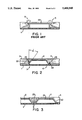
- FIG. 6 depicts a partly cutaway view of a circuit board assembly including, components shielded by a circuit board within a housing in accordance with the present invention
- the angle ( ⁇ ) of inclination from the vertical plane is approximately 20°-40°.
- the most preferred angle of inclination ( ⁇ ) is 30°.
- FIG. 4 illustrates a still further embodiment of the invention in which the soldering pins of the shielding housing have soldering ridges 9.
- soldering pins of the shielding housing have soldering ridges 9.
- FIG. 2 area 6, and in FIG. 3, the housing 2 has been surface-mounted by soldering to the surface of the circuit board 1 in such a manner that the grounding pins are oriented outwardly from the edge of the housing 2.
- Area 7 in FIG. 2 shows how the attachment means can also be oriented inwardly from the edge of the housing 2, in which case more freedom can be provided in the de:sign of the layout of the circuit board.
- Ease of production is specifically improved because the housing design allows the housing to be soldered simultaneously with the components below it.
- the air apertures promote the transfer of heat at the soldering stage to the components beneath the shielding housing, and thereby the success of the soldering is ensured. Without such holes, reflow soldering is slow and uncertain. This means that soldering is achieved, but the heating time is much longer. Long-time high heat may be dangerous for the components used outside the shield. Providing such a long heating period in a hot-air reflow kiln may be difficult.
- Another advantage of the housing 2 is that handling can easily be automated in the same manner as the automatic installation of components on a circuit board.
Abstract
A circuit board assembly including a shielding housing mounted on a circuit board (1), the shielding housing being intended for radio-frequency shieldings. The shielding housing (2) having a wall inclined at an angle α to a plane orthogonal to the plane of the circuit board. The housing of the circuit board assembly being suitable for at least a partial embedding into an exterior wall of an electronic apparatus.
Description
This is a continuation of application Ser. No. 07/945,607, filed on Sep. 16, 1992, now abandoned.
Originally shielding was provided using RF tape. Thereafter housings made from a tinned steel sheet by bending and by soldering the corners were used. The housings were usually affixed to the circuit board manually, normally by manual soldering, the components being accessed by removing or opening the shielding housing.
Opening the shielding housings for inspection and tuning is no longer necessary due to the quality of the state of the art components. Tuning is also achieved by some method other than by turning screws beneath the cover, for example through software or in some other more economical manner.
The most significant characteristics of a housing are ease of assembly and minimum space consumption so that the components of an electronic device may be shielded in an assembly which is easy to manufacture and which may be located within as small a device as possible.
According to a first aspect of the present invention there is provided, a circuit board assembly, comprising a circuit board, electronic components mounted on the circuit board, and at least one housing, for interference shielding, comprising a top surface, a wall and means for attachment to a substantially flat substrate in which a portion of the wall is inclined relative to a plane orthogonal to the plane of the substrate; wherein the housing is mounted on the circuit board and encloses at least some of the electronic components.
In the circuit board assembly the shielding housing, together with the components beneath it, is soldered to the circuit board by soldering pins at its edges, for example by reflow soldering.
An important advantage of the invention is improved production. The work time required is considerably reduced.
The housing can also be embedded into the wall of the casing surrounding the assembly, such as the outer shell of a telephone, saving a considerable amount of space. The outer dimensions of the telephone are therefore reduced without weakening the flow characteristics of the wall in terms of casting techniques.
According to a second aspect of the present invention there is provided an electronic apparatus including a circuit board assembly further comprising an external wall portion, wherein the housing of said assembly is embedded at least partially in said external wall portion.
Even if two or more shielding housings were placed very close to each other and embedded into a wall, owing to the design of the shielding housings there will be left in the wall so-called flow channels which are advantageous in terms of casting techniques. Previously it has not been possible to embed the shielding housings into a wall as in such a case the wall will be weak and of a low visual quality.
Embodiments of the present invention will now be described herewith, by way of example, with reference to the accompanying drawings, in which:
FIG. 1 depicts a prior art shielding housings embedded in a casing in which the wall portion is weak and of a low visual quality.
FIGS. 2 and 3 depict shielding housings according to the invention, embedded into a wall;
FIG. 4 depicts a cross section of a shielding housing according to one embodiment of the present invention;
FIG. 5 depicts a cross section of a housing according to another embodiment of the present invention;
FIG. 6 depicts a partly cutaway view of a circuit board assembly including, components shielded by a circuit board within a housing in accordance with the present invention;
FIG. 7 depicts a shielding housing according to another embodiment of the present invention; and
FIG. 8 depicts prior art rectangular housings are embedded into an exterior wall.
FIGS. 2 to 7 illustrate circuit board assemblies including housings 2 for providing shielding against radio frequency interference, comprising a top surface 21, a wall portion 22 and means 6 and 8 for attachment to a substantially flat substrate 1, in which the wall portion 22 is inclined, at an angle (α) relative to a plane orthogonal to the plane of the substrate 1.
such a housing 2 may also be manufactured by deep drawing or punching and will be dimensionally highly precise, as compared with a housing made by bending metal. Also the requirement for the soldering of the corners of the housing is eliminated.
Furthermore, the structure is more rigid, which facilitates installation by machine, and the attachment of such a housing 2 can be easily automated. The design of the housing 2 enables the housing 2 to be stored in small spaces and at the same time in proper order considering automatic assembling. Owing to the shape of the housing, housings can be positioned very close to each other and soldered by manual soldering.
The angle (α) of inclination from the vertical plane is approximately 20°-40°. The most preferred angle of inclination (α) is 30°.
FIGS. 2 and 3 show a housing 2 embedded into the exterior wall 3 of a casing such as the outer shell of a telephone. Due to the shape of the housing 2, at the time of the casting of the exterior wall 3, the structural material can flow smoothly, in the manner indicated by the arrows 4, and thus as the material fills the space 25 around the inclined wall portion 22. A strong exterior wall 3 may be produced with the housing 2 embedded therein causing the wall thickness, along the top surface 21 of the housing 2 to be thin, the wall gaining strength from the thicker area 25 around the inclined wall portions 22. Therefore, the wall thickness is not excessive, as in the prior art exterior wall 31. The moulding is, furthermore, accomplished with substantially less eddying of the material, in which case the wall will be strong and outwardly visible surface quality flaws (FIG. 1, area 5) can be avoided.
FIG. 8 illustrates a pair of prior art housing 21, as shown in FIG. 1, embedded in an exterior wall, and illustrates the fact that with the said housing 23 the outer exterior wall 31 must be thick to provide the required strength. Thus the prior art housing if embedded in the exterior wall 31 of a telephone will result in the exterior dimensions of the telephone being larger than that possible when the housing 2 is used, see FIG. 3.
FIGS. 6 and 7 illustrate a circuit board assembly, comprising a circuit board 1 and a housing 2 for providing shielding against radio frequency interference, the housing comprising a top surface 21 a wall portion 22 and means 6 for attachment to the circuit board, wherein there are apertures 10,11,13 providing ventilation for the volume within the housing 2.
FIG. 6 illustrates an embodiment wherein the air apertures 13 are located in the circuit board, beneath the housing 2.
FIG. 7 illustrated an embodiment wherein the air apertures 10,11,13 are located in the housing. These air apertures 10,11,13 also serve as cooling holes, and these holes can be made use of in the automation of the production. It is simple to arrange in them so-called gripping points by which it is easy for an automatic device to "grip". If it is necessary to use different housings in a product, it is also easy, by different positioning of the holes 11, to provide automatic identification between the different shielding housings.
FIG. 7 also illustrates an embodiment wherein the air apertures 10 are located between the soldering pins 6 of the housing 2.
FIG. 2 illustrates an embodiment wherein the housing is soldered by a surface joint 7 to the surface of the circuit board i by soldering pins which are oriented outwardly from the edge of the housing. In a further embodiment the hounding 2 is surface mounted by soldering to the surface of the circuit board I by soldering pins 6, some or all of which are oriented inwardly from the edge of the housing.
In a further embodiment the housing 2 is surface mounted by soldering to the surface of the circuit board 1 by soldering pins the edges of which are perpendicular to the surface of the circuit board 1. Embodiments such as these thus allow more freedom in the design of the layout of the circuit board 1.
FIG. 4 illustrates a still further embodiment of the invention in which the soldering pins of the shielding housing have soldering ridges 9. Thus necessary clearances for conductors (not shown), for example, are obtained at the lower edge of the housing 1.
The housing is soldered, simultaneously with the components inside it, to the circuit board, for example in a fellow kiln.
In FIG. 2, area 6, and in FIG. 3, the housing 2 has been surface-mounted by soldering to the surface of the circuit board 1 in such a manner that the grounding pins are oriented outwardly from the edge of the housing 2. Area 7 in FIG. 2 shows how the attachment means can also be oriented inwardly from the edge of the housing 2, in which case more freedom can be provided in the de:sign of the layout of the circuit board.
FIG. 5 depicts an embodiment in which the edge of the housing 2 has separate tags 8 passing through the circuit board 1. Thus the housing 2 can be soldered to the circuit board by these tags 8, namely the attachment means 6.
A further embodiment of the housing as shown in FIG. 4 has soldering ridges 9 in the attachment means of the housing 2 in such a manner that clearance holes 10 for conductors are left between the ridges 9. Also, the housing 2 may have cooling holes 11, normally in the top surface.
Ease of production is specifically improved because the housing design allows the housing to be soldered simultaneously with the components below it. The air apertures promote the transfer of heat at the soldering stage to the components beneath the shielding housing, and thereby the success of the soldering is ensured. Without such holes, reflow soldering is slow and uncertain. This means that soldering is achieved, but the heating time is much longer. Long-time high heat may be dangerous for the components used outside the shield. Providing such a long heating period in a hot-air reflow kiln may be difficult. Another advantage of the housing 2 is that handling can easily be automated in the same manner as the automatic installation of components on a circuit board.
The housing is preferably fabricated from metal sheet, in which case it will have all the properties desired. The housing 2 may also be made of some other electrically conductive material, and if a compromise is made regarding its EMI-shielding properties, also from an electrically non-conductive material.
In view of the foregoing description it will be evident to a person skilled in the art that modifications and improvements may be incorporated without departing from the scope of the present invention.
Claims (1)
1. A method of reflow soldering components to a circuit board comprising steps of:
positioning an interference shielding housing on the circuit board to enclose predetermined electronic components located on the circuit board, the housing having apertures extending through a top surface and located between the circuit board and a bottom edge of the housing and, a substantially solid inclined wall between the bottom edge and top surface that does not have holes; and
heating the circuit board, electronic components and housing by use of hot air, wherein the hot air flows into the apertures at the bottom edge of the housing and out of the housing through the apertures at the top surface with a chimney-like air flow such that the hot air heats solder enclosed by the housing to thereby cause melting and reflow of the solder to simultaneously reflow solder the housing and the enclosed predetermined electronic components to the circuit board.
Priority Applications (2)
| Application Number | Priority Date | Filing Date | Title |
|---|---|---|---|
| US08/183,577 US5400949A (en) | 1991-09-19 | 1994-01-18 | Circuit board assembly |
| US08/345,610 US5442521A (en) | 1991-09-19 | 1994-11-28 | Circuit board assembly |
Applications Claiming Priority (4)
| Application Number | Priority Date | Filing Date | Title |
|---|---|---|---|
| FI914416 | 1991-09-19 | ||
| FI914416A FI109960B (en) | 1991-09-19 | 1991-09-19 | Electronic device |
| US94560792A | 1992-09-16 | 1992-09-16 | |
| US08/183,577 US5400949A (en) | 1991-09-19 | 1994-01-18 | Circuit board assembly |
Related Parent Applications (1)
| Application Number | Title | Priority Date | Filing Date |
|---|---|---|---|
| US94560792A Continuation | 1991-09-19 | 1992-09-16 |
Related Child Applications (1)
| Application Number | Title | Priority Date | Filing Date |
|---|---|---|---|
| US08/345,610 Division US5442521A (en) | 1991-09-19 | 1994-11-28 | Circuit board assembly |
Publications (1)
| Publication Number | Publication Date |
|---|---|
| US5400949A true US5400949A (en) | 1995-03-28 |
Family
ID=8533160
Family Applications (2)
| Application Number | Title | Priority Date | Filing Date |
|---|---|---|---|
| US08/183,577 Expired - Lifetime US5400949A (en) | 1991-09-19 | 1994-01-18 | Circuit board assembly |
| US08/345,610 Expired - Lifetime US5442521A (en) | 1991-09-19 | 1994-11-28 | Circuit board assembly |
Family Applications After (1)
| Application Number | Title | Priority Date | Filing Date |
|---|---|---|---|
| US08/345,610 Expired - Lifetime US5442521A (en) | 1991-09-19 | 1994-11-28 | Circuit board assembly |
Country Status (5)
| Country | Link |
|---|---|
| US (2) | US5400949A (en) |
| EP (1) | EP0519767B1 (en) |
| AT (1) | ATE122532T1 (en) |
| DE (1) | DE69202405T2 (en) |
| FI (1) | FI109960B (en) |
Cited By (81)
| Publication number | Priority date | Publication date | Assignee | Title |
|---|---|---|---|---|
| US5603103A (en) * | 1993-11-26 | 1997-02-11 | Nokia Mobile Phones Ltd. | Radio telephone with compliant shield and method |
| US5621363A (en) * | 1994-10-03 | 1997-04-15 | Motorola, Inc. | Modem having an electromagnetic shield for a controller |
| US5742488A (en) * | 1994-09-07 | 1998-04-21 | Nokia Mobile Phones Limited | Shielding device and method of mounting |
| US5761053A (en) * | 1996-05-08 | 1998-06-02 | W. L. Gore & Associates, Inc. | Faraday cage |
| US5838551A (en) * | 1996-08-01 | 1998-11-17 | Northern Telecom Limited | Electronic package carrying an electronic component and assembly of mother board and electronic package |
| US5844166A (en) * | 1994-06-16 | 1998-12-01 | Nokia Mobile Phones, Ltd. | Lattice RF shield |
| US5895884A (en) * | 1995-02-07 | 1999-04-20 | Nokia Mobile Phones, Ltd. | Shielding device with push fit lid |
| US5911356A (en) * | 1996-08-19 | 1999-06-15 | Sony Corporation | Method for attaching lead parts and shield case to printed circuit board, and method for attaching chip parts, lead parts and shield case to printed circuit board |
| US5917710A (en) * | 1995-05-12 | 1999-06-29 | Nokia Mobile Phones Limited | Electromagnetic shield assembly |
| US5952922A (en) * | 1996-12-31 | 1999-09-14 | Lucent Technologies Inc. | In-building modulated backscatter system |
| US6046683A (en) * | 1996-12-31 | 2000-04-04 | Lucent Technologies Inc. | Modulated backscatter location system |
| US6052045A (en) * | 1999-03-12 | 2000-04-18 | Kearney-National, Inc. | Electromechanical switching device package with controlled impedance environment |
| US6051780A (en) * | 1996-07-19 | 2000-04-18 | Nokia Mobiles Phones Ltd. | Screening device against electromagnetic radiation |
| US6084530A (en) * | 1996-12-30 | 2000-07-04 | Lucent Technologies Inc. | Modulated backscatter sensor system |
| US6110563A (en) * | 1995-12-22 | 2000-08-29 | Nokia Mobile Phones, Ltd. | Method and arrangement for electromagnetically shielding an electronic means |
| US6130623A (en) * | 1996-12-31 | 2000-10-10 | Lucent Technologies Inc. | Encryption for modulated backscatter systems |
| US6178097B1 (en) | 1999-01-22 | 2001-01-23 | Dial Tool Industries, Inc. | RF shield having removable cover |
| US6184841B1 (en) | 1996-12-31 | 2001-02-06 | Lucent Technologies Inc. | Antenna array in an RFID system |
| US6201876B1 (en) | 1997-01-31 | 2001-03-13 | Nokia Mobile Phones Ltd. | Device for protecting a microphone from external disturbances |
| US6235985B1 (en) * | 1998-04-13 | 2001-05-22 | Lucent Technologies, Inc. | Low profile printed circuit board RF shield for radiating pin |
| US6297967B1 (en) | 1997-02-05 | 2001-10-02 | Nokia Mobile Phones Ltd. | Self-securing RF screened housing |
| US6324074B1 (en) | 1997-07-18 | 2001-11-27 | Nokia Mobile Phones Ltd. | Electronic device having a shield member and a shield gasket |
| US6369710B1 (en) | 2000-03-27 | 2002-04-09 | Lucent Technologies Inc. | Wireless security system |
| US6456668B1 (en) | 1996-12-31 | 2002-09-24 | Lucent Technologies Inc. | QPSK modulated backscatter system |
| US6459886B1 (en) | 1997-11-04 | 2002-10-01 | Nokia Mobile Phones Limited | Communication terminal with a partition wall |
| US6499215B1 (en) * | 2000-06-29 | 2002-12-31 | International Business Machines Corporation | Processing of circuit boards with protective, adhesive-less covers on area array bonding sites |
| EP1320077A2 (en) * | 2001-12-15 | 2003-06-18 | Francotyp-Postalia AG & Co. KG | Security Housing |
| US20030169138A1 (en) * | 2002-03-08 | 2003-09-11 | Motta James J. | Surface mount molded relay package and method of manufacturing same |
| US6621910B1 (en) | 1997-10-06 | 2003-09-16 | Nokia Mobile Phones Ltd. | Method and arrangement for improving leak tolerance of an earpiece in a radio device |
| US20030223211A1 (en) * | 2002-05-30 | 2003-12-04 | Hannstar Display Corp. | Electromagnetic interference (EMI) shield structure |
| USRE38381E1 (en) | 2000-07-21 | 2004-01-13 | Kearney-National Inc. | Inverted board mounted electromechanical device |
| US20040150977A1 (en) * | 2003-01-20 | 2004-08-05 | Chia-Ming Hsieh | Ball grid array package with an electromagnetic shield connected directly to a printed circuit board |
| US20040162143A1 (en) * | 2000-06-07 | 2004-08-19 | Toru Morita | Program execution system, program execution device, relay device, and recording medium |
| US20040165369A1 (en) * | 2003-02-13 | 2004-08-26 | Lionetta William G. | Combination metal and plastic EMI shield |
| US7005573B2 (en) | 2003-02-13 | 2006-02-28 | Parker-Hannifin Corporation | Composite EMI shield |
| US20060086518A1 (en) * | 2003-03-31 | 2006-04-27 | Toshiyuki Kawaguchi | Shield box and shield method |
| US20060172570A1 (en) * | 2005-01-31 | 2006-08-03 | Minich Steven E | Surface-mount connector |
| US20060223362A1 (en) * | 2005-04-05 | 2006-10-05 | Swain Wilfred J | Electrical connector with cooling features |
| US20060228948A1 (en) * | 2004-12-22 | 2006-10-12 | Swain Wilfred J | Electrical power connector |
| US20060228927A1 (en) * | 2003-12-31 | 2006-10-12 | Fci Americas Technology | Electrical power contacts and connectors comprising same |
| US20070014092A1 (en) * | 2001-06-12 | 2007-01-18 | Naoya Tanaka | Resin-packaged protection circuit module for rechargeable batteries and method of making the same |
| US20070197063A1 (en) * | 2006-02-21 | 2007-08-23 | Ngo Hung V | Electrical connectors having power contacts with alignment and/or restraining features |
| US20070275586A1 (en) * | 2006-05-26 | 2007-11-29 | Ngo Hung V | Connectors and contacts for transmitting electrical power |
| US20080000683A1 (en) * | 2004-01-29 | 2008-01-03 | Igor Vinokor | Ultra-low height electromagnetic shielding enclosure |
| US20080248680A1 (en) * | 2007-04-04 | 2008-10-09 | Fci Americas Technology, Inc. | Power cable connector |
| US20080293267A1 (en) * | 2007-05-21 | 2008-11-27 | Fci | Electrical connector with stress-distribution features |
| US20080292846A1 (en) * | 2007-05-21 | 2008-11-27 | Fujitsu Media Devices Limited | Electronic component and manufacturing method therefor |
| USD608293S1 (en) | 2009-01-16 | 2010-01-19 | Fci Americas Technology, Inc. | Vertical electrical connector |
| US20100029126A1 (en) * | 2008-07-29 | 2010-02-04 | Hung Viet Ngo | Electrical communication system having latching and strain relief features |
| USD610548S1 (en) | 2009-01-16 | 2010-02-23 | Fci Americas Technology, Inc. | Right-angle electrical connector |
| USRE41283E1 (en) | 2003-01-28 | 2010-04-27 | Fci Americas Technology, Inc. | Power connector with safety feature |
| US7726982B2 (en) | 2006-06-15 | 2010-06-01 | Fci Americas Technology, Inc. | Electrical connectors with air-circulation features |
| USD618180S1 (en) | 2009-04-03 | 2010-06-22 | Fci Americas Technology, Inc. | Asymmetrical electrical connector |
| USD618181S1 (en) | 2009-04-03 | 2010-06-22 | Fci Americas Technology, Inc. | Asymmetrical electrical connector |
| USD619099S1 (en) | 2009-01-30 | 2010-07-06 | Fci Americas Technology, Inc. | Electrical connector |
| US7762857B2 (en) | 2007-10-01 | 2010-07-27 | Fci Americas Technology, Inc. | Power connectors with contact-retention features |
| US20100197166A1 (en) * | 2009-01-30 | 2010-08-05 | Hung Viet Ngo | Electrical connector having power contacts |
| USD640637S1 (en) | 2009-01-16 | 2011-06-28 | Fci Americas Technology Llc | Vertical electrical connector |
| USD641709S1 (en) | 2009-01-16 | 2011-07-19 | Fci Americas Technology Llc | Vertical electrical connector |
| USD664096S1 (en) | 2009-01-16 | 2012-07-24 | Fci Americas Technology Llc | Vertical electrical connector |
| US20120314385A1 (en) * | 2011-06-07 | 2012-12-13 | Sony Corporation | Circuit board and electronic apparatus |
| USD718253S1 (en) | 2012-04-13 | 2014-11-25 | Fci Americas Technology Llc | Electrical cable connector |
| US8905651B2 (en) | 2012-01-31 | 2014-12-09 | Fci | Dismountable optical coupling device |
| USD720698S1 (en) | 2013-03-15 | 2015-01-06 | Fci Americas Technology Llc | Electrical cable connector |
| US8944831B2 (en) | 2012-04-13 | 2015-02-03 | Fci Americas Technology Llc | Electrical connector having ribbed ground plate with engagement members |
| US9006880B1 (en) | 2000-11-28 | 2015-04-14 | Knowles Electronics, Llc | Top port multi-part surface mount silicon condenser microphone |
| USD727268S1 (en) | 2012-04-13 | 2015-04-21 | Fci Americas Technology Llc | Vertical electrical connector |
| USD727852S1 (en) | 2012-04-13 | 2015-04-28 | Fci Americas Technology Llc | Ground shield for a right angle electrical connector |
| US9040360B1 (en) | 2000-11-28 | 2015-05-26 | Knowles Electronics, Llc | Methods of manufacture of bottom port multi-part surface mount MEMS microphones |
| US9048583B2 (en) | 2009-03-19 | 2015-06-02 | Fci Americas Technology Llc | Electrical connector having ribbed ground plate |
| USD733662S1 (en) | 2013-01-25 | 2015-07-07 | Fci Americas Technology Llc | Connector housing for electrical connector |
| US9078063B2 (en) | 2012-08-10 | 2015-07-07 | Knowles Electronics, Llc | Microphone assembly with barrier to prevent contaminant infiltration |
| USD746236S1 (en) | 2012-07-11 | 2015-12-29 | Fci Americas Technology Llc | Electrical connector housing |
| US9257778B2 (en) | 2012-04-13 | 2016-02-09 | Fci Americas Technology | High speed electrical connector |
| US9374643B2 (en) | 2011-11-04 | 2016-06-21 | Knowles Electronics, Llc | Embedded dielectric as a barrier in an acoustic device and method of manufacture |
| US9543703B2 (en) | 2012-07-11 | 2017-01-10 | Fci Americas Technology Llc | Electrical connector with reduced stack height |
| US9794661B2 (en) | 2015-08-07 | 2017-10-17 | Knowles Electronics, Llc | Ingress protection for reducing particle infiltration into acoustic chamber of a MEMS microphone package |
| US9980368B2 (en) | 2015-08-18 | 2018-05-22 | Foxcomm Interconnect Technology Limited | Detachable shielding device |
| US20210051825A1 (en) * | 2018-06-15 | 2021-02-18 | Hewlett-Packard Development Company, L.P. | Circuit board assemblies |
| US20210307220A1 (en) * | 2020-03-27 | 2021-09-30 | Lapis Semiconductor Co., Ltd. | Shield case |
| US11432442B2 (en) | 2018-10-03 | 2022-08-30 | Interplex Industries, Inc. | EMC shield and method of producing the same |
Families Citing this family (22)
| Publication number | Priority date | Publication date | Assignee | Title |
|---|---|---|---|---|
| FI109960B (en) * | 1991-09-19 | 2002-10-31 | Nokia Corp | Electronic device |
| DE4236593A1 (en) * | 1992-10-29 | 1994-05-05 | Siemens Ag | Backplane circuit board for a module frame |
| KR0175000B1 (en) * | 1994-12-14 | 1999-02-01 | 윤종용 | Semiconductor device having electromagnetic waves control structure |
| DE29505327U1 (en) * | 1995-03-29 | 1995-08-03 | Siemens Ag | Shielding for logic and high frequency circuits |
| DE19522455A1 (en) * | 1995-06-21 | 1997-01-02 | Telefunken Microelectron | Electromagnetic compatibility screening of electronic components esp. integrated circuits in motor vehicles |
| TW486238U (en) * | 1996-08-18 | 2002-05-01 | Helmut Kahl | Shielding cap |
| SE511426C2 (en) | 1996-10-28 | 1999-09-27 | Ericsson Telefon Ab L M | Apparatus and method of shielding electronics |
| US6491528B1 (en) * | 1998-12-24 | 2002-12-10 | At&T Wireless Services, Inc. | Method and apparatus for vibration and temperature isolation |
| US6191360B1 (en) * | 1999-04-26 | 2001-02-20 | Advanced Semiconductor Engineering, Inc. | Thermally enhanced BGA package |
| DE10026353A1 (en) | 2000-05-27 | 2001-11-29 | Mannesmann Vdo Ag | Shielded electronic circuit |
| CN1905851B (en) * | 2004-01-27 | 2010-11-17 | Xo卡雷公司 | A dental practice operating system |
| EP1826867A1 (en) * | 2006-02-22 | 2007-08-29 | Alps Electric Co., Ltd. | Antenna-integrated module |
| US20080002384A1 (en) * | 2006-06-30 | 2008-01-03 | Motorola, Inc. | Apparatus for providing radio frequency shielding and heat dissipation for electronic components |
| US20080143608A1 (en) * | 2006-12-13 | 2008-06-19 | Alps Electric Co., Ltd. | Antenna-integrated module |
| FR2934749B1 (en) * | 2008-07-31 | 2010-08-27 | Wavecom | DEVICE FOR ELECTROMAGNETIC SHIELDING AND HEAT DISSIPATION DISENGAGED BY AN ELECTRONIC COMPONENT AND CORRESPONDING ELECTRONIC CIRCUIT. |
| EP2197258A1 (en) * | 2008-12-12 | 2010-06-16 | BAE Systems PLC | Shield |
| DK2374340T3 (en) * | 2008-12-12 | 2017-07-17 | Bae Systems Plc | Screen |
| DE102009033258B4 (en) * | 2009-07-14 | 2019-01-10 | Sew-Eurodrive Gmbh & Co Kg | casing |
| US20170215305A1 (en) * | 2016-01-27 | 2017-07-27 | Raymond Kirk Price | Emi shield for an electronic optical device |
| DE102016001617A1 (en) | 2016-02-14 | 2017-08-17 | Efkon Ag | Shielding device for an antenna arrangement of a vehicle toll collection device |
| DE102017208076A1 (en) * | 2017-05-12 | 2018-11-15 | Magna Powertrain Bad Homburg GmbH | Component with EMC protection for electronic board |
| CN113615328B (en) * | 2019-03-28 | 2023-10-20 | 三菱电机株式会社 | shielding shell |
Citations (12)
| Publication number | Priority date | Publication date | Assignee | Title |
|---|---|---|---|---|
| US4370515A (en) * | 1979-12-26 | 1983-01-25 | Rockwell International Corporation | Electromagnetic interference |
| US4410874A (en) * | 1975-03-03 | 1983-10-18 | Hughes Aircraft Company | Large area hybrid microcircuit assembly |
| US4517738A (en) * | 1982-04-24 | 1985-05-21 | Tokyo Shibaura Denki Kabushiki Kaisha | Method for packaging electronic parts |
| JPS60148158A (en) * | 1984-01-12 | 1985-08-05 | Nec Corp | Hybrid integrated circuit |
| US4626963A (en) * | 1985-02-28 | 1986-12-02 | Rca Corporation | Wave solderable RF shield member for a printed circuit board |
| EP0262332A2 (en) * | 1986-08-01 | 1988-04-06 | Siemens Aktiengesellschaft | Printed circuit board for communication art |
| US4839774A (en) * | 1988-01-25 | 1989-06-13 | Digital Equipment Corporation | Apparatus and method for cooling electronic component packages using an array of directed nozzles fabricated in the circuit board |
| US4838475A (en) * | 1987-08-28 | 1989-06-13 | Motorola, Inc. | Method and apparatus for EMI/RFI shielding an infrared energy reflow soldered device |
| FR2629664A1 (en) * | 1988-04-02 | 1989-10-06 | Messerschmitt Boelkow Blohm | HOUSING FOR HYBRID CIRCUITS |
| JPH03206691A (en) * | 1990-01-08 | 1991-09-10 | Nec Corp | Hybrid integrated circuit |
| EP0519768A2 (en) * | 1991-05-21 | 1992-12-23 | Thomson-Csf | High density information storage carrier and method of reading such a carrier |
| FI914416A (en) * | 1991-09-19 | 1993-03-20 | Nokia Mobile Phones Ltd | FOERFARANDE FOER FASTSAETTNING AV EN SKYDDSKAOPA PAO KRETSKORT OCH SKYDDSKAOPA |
Family Cites Families (2)
| Publication number | Priority date | Publication date | Assignee | Title |
|---|---|---|---|---|
| JPH03195094A (en) * | 1989-12-25 | 1991-08-26 | Nippon Chemicon Corp | Shield structure of circuit device |
| JPH04179256A (en) * | 1990-11-13 | 1992-06-25 | Mitsubishi Electric Corp | Semiconductor device |
-
1991
- 1991-09-19 FI FI914416A patent/FI109960B/en active
-
1992
- 1992-09-17 DE DE69202405T patent/DE69202405T2/en not_active Expired - Lifetime
- 1992-09-17 EP EP92308478A patent/EP0519767B1/en not_active Expired - Lifetime
- 1992-09-17 AT AT92308478T patent/ATE122532T1/en not_active IP Right Cessation
-
1994
- 1994-01-18 US US08/183,577 patent/US5400949A/en not_active Expired - Lifetime
- 1994-11-28 US US08/345,610 patent/US5442521A/en not_active Expired - Lifetime
Patent Citations (12)
| Publication number | Priority date | Publication date | Assignee | Title |
|---|---|---|---|---|
| US4410874A (en) * | 1975-03-03 | 1983-10-18 | Hughes Aircraft Company | Large area hybrid microcircuit assembly |
| US4370515A (en) * | 1979-12-26 | 1983-01-25 | Rockwell International Corporation | Electromagnetic interference |
| US4517738A (en) * | 1982-04-24 | 1985-05-21 | Tokyo Shibaura Denki Kabushiki Kaisha | Method for packaging electronic parts |
| JPS60148158A (en) * | 1984-01-12 | 1985-08-05 | Nec Corp | Hybrid integrated circuit |
| US4626963A (en) * | 1985-02-28 | 1986-12-02 | Rca Corporation | Wave solderable RF shield member for a printed circuit board |
| EP0262332A2 (en) * | 1986-08-01 | 1988-04-06 | Siemens Aktiengesellschaft | Printed circuit board for communication art |
| US4838475A (en) * | 1987-08-28 | 1989-06-13 | Motorola, Inc. | Method and apparatus for EMI/RFI shielding an infrared energy reflow soldered device |
| US4839774A (en) * | 1988-01-25 | 1989-06-13 | Digital Equipment Corporation | Apparatus and method for cooling electronic component packages using an array of directed nozzles fabricated in the circuit board |
| FR2629664A1 (en) * | 1988-04-02 | 1989-10-06 | Messerschmitt Boelkow Blohm | HOUSING FOR HYBRID CIRCUITS |
| JPH03206691A (en) * | 1990-01-08 | 1991-09-10 | Nec Corp | Hybrid integrated circuit |
| EP0519768A2 (en) * | 1991-05-21 | 1992-12-23 | Thomson-Csf | High density information storage carrier and method of reading such a carrier |
| FI914416A (en) * | 1991-09-19 | 1993-03-20 | Nokia Mobile Phones Ltd | FOERFARANDE FOER FASTSAETTNING AV EN SKYDDSKAOPA PAO KRETSKORT OCH SKYDDSKAOPA |
Cited By (147)
| Publication number | Priority date | Publication date | Assignee | Title |
|---|---|---|---|---|
| US5603103A (en) * | 1993-11-26 | 1997-02-11 | Nokia Mobile Phones Ltd. | Radio telephone with compliant shield and method |
| US5844166A (en) * | 1994-06-16 | 1998-12-01 | Nokia Mobile Phones, Ltd. | Lattice RF shield |
| US5742488A (en) * | 1994-09-07 | 1998-04-21 | Nokia Mobile Phones Limited | Shielding device and method of mounting |
| US5621363A (en) * | 1994-10-03 | 1997-04-15 | Motorola, Inc. | Modem having an electromagnetic shield for a controller |
| US5895884A (en) * | 1995-02-07 | 1999-04-20 | Nokia Mobile Phones, Ltd. | Shielding device with push fit lid |
| US5917710A (en) * | 1995-05-12 | 1999-06-29 | Nokia Mobile Phones Limited | Electromagnetic shield assembly |
| US6110563A (en) * | 1995-12-22 | 2000-08-29 | Nokia Mobile Phones, Ltd. | Method and arrangement for electromagnetically shielding an electronic means |
| US5761053A (en) * | 1996-05-08 | 1998-06-02 | W. L. Gore & Associates, Inc. | Faraday cage |
| US6051780A (en) * | 1996-07-19 | 2000-04-18 | Nokia Mobiles Phones Ltd. | Screening device against electromagnetic radiation |
| US5838551A (en) * | 1996-08-01 | 1998-11-17 | Northern Telecom Limited | Electronic package carrying an electronic component and assembly of mother board and electronic package |
| US5911356A (en) * | 1996-08-19 | 1999-06-15 | Sony Corporation | Method for attaching lead parts and shield case to printed circuit board, and method for attaching chip parts, lead parts and shield case to printed circuit board |
| US6084530A (en) * | 1996-12-30 | 2000-07-04 | Lucent Technologies Inc. | Modulated backscatter sensor system |
| US6456668B1 (en) | 1996-12-31 | 2002-09-24 | Lucent Technologies Inc. | QPSK modulated backscatter system |
| US5952922A (en) * | 1996-12-31 | 1999-09-14 | Lucent Technologies Inc. | In-building modulated backscatter system |
| US6130623A (en) * | 1996-12-31 | 2000-10-10 | Lucent Technologies Inc. | Encryption for modulated backscatter systems |
| US6046683A (en) * | 1996-12-31 | 2000-04-04 | Lucent Technologies Inc. | Modulated backscatter location system |
| US6184841B1 (en) | 1996-12-31 | 2001-02-06 | Lucent Technologies Inc. | Antenna array in an RFID system |
| US6201876B1 (en) | 1997-01-31 | 2001-03-13 | Nokia Mobile Phones Ltd. | Device for protecting a microphone from external disturbances |
| US6297967B1 (en) | 1997-02-05 | 2001-10-02 | Nokia Mobile Phones Ltd. | Self-securing RF screened housing |
| US6324074B1 (en) | 1997-07-18 | 2001-11-27 | Nokia Mobile Phones Ltd. | Electronic device having a shield member and a shield gasket |
| US6621910B1 (en) | 1997-10-06 | 2003-09-16 | Nokia Mobile Phones Ltd. | Method and arrangement for improving leak tolerance of an earpiece in a radio device |
| US6459886B1 (en) | 1997-11-04 | 2002-10-01 | Nokia Mobile Phones Limited | Communication terminal with a partition wall |
| US6235985B1 (en) * | 1998-04-13 | 2001-05-22 | Lucent Technologies, Inc. | Low profile printed circuit board RF shield for radiating pin |
| US6178097B1 (en) | 1999-01-22 | 2001-01-23 | Dial Tool Industries, Inc. | RF shield having removable cover |
| US6052045A (en) * | 1999-03-12 | 2000-04-18 | Kearney-National, Inc. | Electromechanical switching device package with controlled impedance environment |
| US6369710B1 (en) | 2000-03-27 | 2002-04-09 | Lucent Technologies Inc. | Wireless security system |
| US20040162143A1 (en) * | 2000-06-07 | 2004-08-19 | Toru Morita | Program execution system, program execution device, relay device, and recording medium |
| US6499215B1 (en) * | 2000-06-29 | 2002-12-31 | International Business Machines Corporation | Processing of circuit boards with protective, adhesive-less covers on area array bonding sites |
| US6700068B2 (en) | 2000-06-29 | 2004-03-02 | International Business Machines Corporation | Adhesive-less cover on area array bonding site of circuit board |
| USRE38381E1 (en) | 2000-07-21 | 2004-01-13 | Kearney-National Inc. | Inverted board mounted electromechanical device |
| US9150409B1 (en) | 2000-11-28 | 2015-10-06 | Knowles Electronics, Llc | Methods of manufacture of bottom port surface mount MEMS microphones |
| US9067780B1 (en) | 2000-11-28 | 2015-06-30 | Knowles Electronics, Llc | Methods of manufacture of top port surface mount MEMS microphones |
| US10321226B2 (en) | 2000-11-28 | 2019-06-11 | Knowles Electronics, Llc | Top port multi-part surface mount MEMS microphone |
| US9006880B1 (en) | 2000-11-28 | 2015-04-14 | Knowles Electronics, Llc | Top port multi-part surface mount silicon condenser microphone |
| US9980038B2 (en) | 2000-11-28 | 2018-05-22 | Knowles Electronics, Llc | Top port multi-part surface mount silicon condenser microphone |
| US9024432B1 (en) | 2000-11-28 | 2015-05-05 | Knowles Electronics, Llc | Bottom port multi-part surface mount MEMS microphone |
| US9023689B1 (en) | 2000-11-28 | 2015-05-05 | Knowles Electronics, Llc | Top port multi-part surface mount MEMS microphone |
| US9338560B1 (en) | 2000-11-28 | 2016-05-10 | Knowles Electronics, Llc | Top port multi-part surface mount silicon condenser microphone |
| US9156684B1 (en) | 2000-11-28 | 2015-10-13 | Knowles Electronics, Llc | Methods of manufacture of top port surface mount MEMS microphones |
| US9040360B1 (en) | 2000-11-28 | 2015-05-26 | Knowles Electronics, Llc | Methods of manufacture of bottom port multi-part surface mount MEMS microphones |
| US9148731B1 (en) | 2000-11-28 | 2015-09-29 | Knowles Electronics, Llc | Top port surface mount MEMS microphone |
| US9139422B1 (en) | 2000-11-28 | 2015-09-22 | Knowles Electronics, Llc | Bottom port surface mount MEMS microphone |
| US9139421B1 (en) | 2000-11-28 | 2015-09-22 | Knowles Electronics, Llc | Top port surface mount MEMS microphone |
| US9051171B1 (en) | 2000-11-28 | 2015-06-09 | Knowles Electronics, Llc | Bottom port surface mount MEMS microphone |
| US9133020B1 (en) | 2000-11-28 | 2015-09-15 | Knowles Electronics, Llc | Methods of manufacture of bottom port surface mount MEMS microphones |
| US9096423B1 (en) | 2000-11-28 | 2015-08-04 | Knowles Electronics, Llc | Methods of manufacture of top port multi-part surface mount MEMS microphones |
| US9061893B1 (en) | 2000-11-28 | 2015-06-23 | Knowles Electronics, Llc | Methods of manufacture of top port multi-part surface mount silicon condenser microphones |
| US20070014092A1 (en) * | 2001-06-12 | 2007-01-18 | Naoya Tanaka | Resin-packaged protection circuit module for rechargeable batteries and method of making the same |
| US7657998B2 (en) * | 2001-12-06 | 2010-02-09 | Rohm Co., Ltd. | Method of making a resin-packaged protection circuit module for rechargeable batteries |
| EP1320077A2 (en) * | 2001-12-15 | 2003-06-18 | Francotyp-Postalia AG & Co. KG | Security Housing |
| US20030169138A1 (en) * | 2002-03-08 | 2003-09-11 | Motta James J. | Surface mount molded relay package and method of manufacturing same |
| US20030223211A1 (en) * | 2002-05-30 | 2003-12-04 | Hannstar Display Corp. | Electromagnetic interference (EMI) shield structure |
| US6859371B2 (en) * | 2002-05-30 | 2005-02-22 | Hannstar Display Corp. | Electromagnetic interference (EMI) shield structure |
| US6947295B2 (en) * | 2003-01-20 | 2005-09-20 | Benq Corporation | Ball grid array package with an electromagnetic shield connected directly to a printed circuit board |
| US20040150977A1 (en) * | 2003-01-20 | 2004-08-05 | Chia-Ming Hsieh | Ball grid array package with an electromagnetic shield connected directly to a printed circuit board |
| USRE41283E1 (en) | 2003-01-28 | 2010-04-27 | Fci Americas Technology, Inc. | Power connector with safety feature |
| US7326862B2 (en) | 2003-02-13 | 2008-02-05 | Parker-Hannifin Corporation | Combination metal and plastic EMI shield |
| US7005573B2 (en) | 2003-02-13 | 2006-02-28 | Parker-Hannifin Corporation | Composite EMI shield |
| US20040165369A1 (en) * | 2003-02-13 | 2004-08-26 | Lionetta William G. | Combination metal and plastic EMI shield |
| US20060086518A1 (en) * | 2003-03-31 | 2006-04-27 | Toshiyuki Kawaguchi | Shield box and shield method |
| US20070202748A1 (en) * | 2003-12-31 | 2007-08-30 | Fci Americas Technology, Inc. | Electrical power contacts and connectors comprising same |
| US7862359B2 (en) | 2003-12-31 | 2011-01-04 | Fci Americas Technology Llc | Electrical power contacts and connectors comprising same |
| US8062046B2 (en) | 2003-12-31 | 2011-11-22 | Fci Americas Technology Llc | Electrical power contacts and connectors comprising same |
| US20090042417A1 (en) * | 2003-12-31 | 2009-02-12 | Hung Viet Ngo | Electrical connectors having power contacts with alignment/or restraining features |
| US7775822B2 (en) | 2003-12-31 | 2010-08-17 | Fci Americas Technology, Inc. | Electrical connectors having power contacts with alignment/or restraining features |
| US20080248670A1 (en) * | 2003-12-31 | 2008-10-09 | Fci Americas Technology, Inc. | Electrical power contacts and connectors comprising same |
| US20060228927A1 (en) * | 2003-12-31 | 2006-10-12 | Fci Americas Technology | Electrical power contacts and connectors comprising same |
| US7452249B2 (en) | 2003-12-31 | 2008-11-18 | Fci Americas Technology, Inc. | Electrical power contacts and connectors comprising same |
| US7402064B2 (en) | 2003-12-31 | 2008-07-22 | Fci Americas Technology, Inc. | Electrical power contacts and connectors comprising same |
| US8187017B2 (en) | 2003-12-31 | 2012-05-29 | Fci Americas Technology Llc | Electrical power contacts and connectors comprising same |
| US20100048056A1 (en) * | 2003-12-31 | 2010-02-25 | Fci Americas Technology, Inc. | Electrical Power Contacts and Connectors Comprising Same |
| US7690937B2 (en) | 2003-12-31 | 2010-04-06 | Fci Americas Technology, Inc. | Electrical power contacts and connectors comprising same |
| US7345248B2 (en) * | 2004-01-29 | 2008-03-18 | Laird Technologies, Inc. | Ultra-low height electromagnetic shielding enclosure |
| US20080000683A1 (en) * | 2004-01-29 | 2008-01-03 | Igor Vinokor | Ultra-low height electromagnetic shielding enclosure |
| US20060228948A1 (en) * | 2004-12-22 | 2006-10-12 | Swain Wilfred J | Electrical power connector |
| US7476108B2 (en) | 2004-12-22 | 2009-01-13 | Fci Americas Technology, Inc. | Electrical power connectors with cooling features |
| US7384289B2 (en) | 2005-01-31 | 2008-06-10 | Fci Americas Technology, Inc. | Surface-mount connector |
| US20080207038A1 (en) * | 2005-01-31 | 2008-08-28 | Fci Americas Technology, Inc. | Surface-mount connector |
| US7749009B2 (en) | 2005-01-31 | 2010-07-06 | Fci Americas Technology, Inc. | Surface-mount connector |
| US20060172570A1 (en) * | 2005-01-31 | 2006-08-03 | Minich Steven E | Surface-mount connector |
| US7541135B2 (en) | 2005-04-05 | 2009-06-02 | Fci Americas Technology, Inc. | Power contact having conductive plates with curved portions contact beams and board tails |
| US7303427B2 (en) | 2005-04-05 | 2007-12-04 | Fci Americas Technology, Inc. | Electrical connector with air-circulation features |
| US20060223362A1 (en) * | 2005-04-05 | 2006-10-05 | Swain Wilfred J | Electrical connector with cooling features |
| US20080038956A1 (en) * | 2005-04-05 | 2008-02-14 | Fci Americas Technology, Inc. | Electrical connector with air-circulation features |
| US7458839B2 (en) | 2006-02-21 | 2008-12-02 | Fci Americas Technology, Inc. | Electrical connectors having power contacts with alignment and/or restraining features |
| US20070197063A1 (en) * | 2006-02-21 | 2007-08-23 | Ngo Hung V | Electrical connectors having power contacts with alignment and/or restraining features |
| US20070275586A1 (en) * | 2006-05-26 | 2007-11-29 | Ngo Hung V | Connectors and contacts for transmitting electrical power |
| US7425145B2 (en) | 2006-05-26 | 2008-09-16 | Fci Americas Technology, Inc. | Connectors and contacts for transmitting electrical power |
| US7726982B2 (en) | 2006-06-15 | 2010-06-01 | Fci Americas Technology, Inc. | Electrical connectors with air-circulation features |
| US20080248680A1 (en) * | 2007-04-04 | 2008-10-09 | Fci Americas Technology, Inc. | Power cable connector |
| US7641500B2 (en) | 2007-04-04 | 2010-01-05 | Fci Americas Technology, Inc. | Power cable connector system |
| US7905731B2 (en) | 2007-05-21 | 2011-03-15 | Fci Americas Technology, Inc. | Electrical connector with stress-distribution features |
| US8199527B2 (en) * | 2007-05-21 | 2012-06-12 | Taiyo Yuden Co., Ltd. | Electronic component and manufacturing method therefor |
| US20080292846A1 (en) * | 2007-05-21 | 2008-11-27 | Fujitsu Media Devices Limited | Electronic component and manufacturing method therefor |
| US20080293267A1 (en) * | 2007-05-21 | 2008-11-27 | Fci | Electrical connector with stress-distribution features |
| US7762857B2 (en) | 2007-10-01 | 2010-07-27 | Fci Americas Technology, Inc. | Power connectors with contact-retention features |
| US20100029126A1 (en) * | 2008-07-29 | 2010-02-04 | Hung Viet Ngo | Electrical communication system having latching and strain relief features |
| US8062051B2 (en) | 2008-07-29 | 2011-11-22 | Fci Americas Technology Llc | Electrical communication system having latching and strain relief features |
| USD647058S1 (en) | 2009-01-16 | 2011-10-18 | Fci Americas Technology Llc | Vertical electrical connector |
| USD610548S1 (en) | 2009-01-16 | 2010-02-23 | Fci Americas Technology, Inc. | Right-angle electrical connector |
| USD696199S1 (en) | 2009-01-16 | 2013-12-24 | Fci Americas Technology Llc | Vertical electrical connector |
| USD664096S1 (en) | 2009-01-16 | 2012-07-24 | Fci Americas Technology Llc | Vertical electrical connector |
| USD608293S1 (en) | 2009-01-16 | 2010-01-19 | Fci Americas Technology, Inc. | Vertical electrical connector |
| USD660245S1 (en) | 2009-01-16 | 2012-05-22 | Fci Americas Technology Llc | Vertical electrical connector |
| USD651981S1 (en) | 2009-01-16 | 2012-01-10 | Fci Americas Technology Llc | Vertical electrical connector |
| USD641709S1 (en) | 2009-01-16 | 2011-07-19 | Fci Americas Technology Llc | Vertical electrical connector |
| USD640637S1 (en) | 2009-01-16 | 2011-06-28 | Fci Americas Technology Llc | Vertical electrical connector |
| US8323049B2 (en) | 2009-01-30 | 2012-12-04 | Fci Americas Technology Llc | Electrical connector having power contacts |
| USD619099S1 (en) | 2009-01-30 | 2010-07-06 | Fci Americas Technology, Inc. | Electrical connector |
| US20100197166A1 (en) * | 2009-01-30 | 2010-08-05 | Hung Viet Ngo | Electrical connector having power contacts |
| US9048583B2 (en) | 2009-03-19 | 2015-06-02 | Fci Americas Technology Llc | Electrical connector having ribbed ground plate |
| US9461410B2 (en) | 2009-03-19 | 2016-10-04 | Fci Americas Technology Llc | Electrical connector having ribbed ground plate |
| US10096921B2 (en) | 2009-03-19 | 2018-10-09 | Fci Usa Llc | Electrical connector having ribbed ground plate |
| US10720721B2 (en) | 2009-03-19 | 2020-07-21 | Fci Usa Llc | Electrical connector having ribbed ground plate |
| USD653621S1 (en) | 2009-04-03 | 2012-02-07 | Fci Americas Technology Llc | Asymmetrical electrical connector |
| USD618180S1 (en) | 2009-04-03 | 2010-06-22 | Fci Americas Technology, Inc. | Asymmetrical electrical connector |
| USD618181S1 (en) | 2009-04-03 | 2010-06-22 | Fci Americas Technology, Inc. | Asymmetrical electrical connector |
| US20120314385A1 (en) * | 2011-06-07 | 2012-12-13 | Sony Corporation | Circuit board and electronic apparatus |
| US9374643B2 (en) | 2011-11-04 | 2016-06-21 | Knowles Electronics, Llc | Embedded dielectric as a barrier in an acoustic device and method of manufacture |
| US8905651B2 (en) | 2012-01-31 | 2014-12-09 | Fci | Dismountable optical coupling device |
| US8944831B2 (en) | 2012-04-13 | 2015-02-03 | Fci Americas Technology Llc | Electrical connector having ribbed ground plate with engagement members |
| USD727852S1 (en) | 2012-04-13 | 2015-04-28 | Fci Americas Technology Llc | Ground shield for a right angle electrical connector |
| USD748063S1 (en) | 2012-04-13 | 2016-01-26 | Fci Americas Technology Llc | Electrical ground shield |
| US9257778B2 (en) | 2012-04-13 | 2016-02-09 | Fci Americas Technology | High speed electrical connector |
| USD750030S1 (en) | 2012-04-13 | 2016-02-23 | Fci Americas Technology Llc | Electrical cable connector |
| USD750025S1 (en) | 2012-04-13 | 2016-02-23 | Fci Americas Technology Llc | Vertical electrical connector |
| USD718253S1 (en) | 2012-04-13 | 2014-11-25 | Fci Americas Technology Llc | Electrical cable connector |
| USD727268S1 (en) | 2012-04-13 | 2015-04-21 | Fci Americas Technology Llc | Vertical electrical connector |
| USD816044S1 (en) | 2012-04-13 | 2018-04-24 | Fci Americas Technology Llc | Electrical cable connector |
| US9831605B2 (en) | 2012-04-13 | 2017-11-28 | Fci Americas Technology Llc | High speed electrical connector |
| USD790471S1 (en) | 2012-04-13 | 2017-06-27 | Fci Americas Technology Llc | Vertical electrical connector |
| US9871323B2 (en) | 2012-07-11 | 2018-01-16 | Fci Americas Technology Llc | Electrical connector with reduced stack height |
| US9543703B2 (en) | 2012-07-11 | 2017-01-10 | Fci Americas Technology Llc | Electrical connector with reduced stack height |
| USD751507S1 (en) | 2012-07-11 | 2016-03-15 | Fci Americas Technology Llc | Electrical connector |
| USD746236S1 (en) | 2012-07-11 | 2015-12-29 | Fci Americas Technology Llc | Electrical connector housing |
| US9078063B2 (en) | 2012-08-10 | 2015-07-07 | Knowles Electronics, Llc | Microphone assembly with barrier to prevent contaminant infiltration |
| USD766832S1 (en) | 2013-01-25 | 2016-09-20 | Fci Americas Technology Llc | Electrical connector |
| USD772168S1 (en) | 2013-01-25 | 2016-11-22 | Fci Americas Technology Llc | Connector housing for electrical connector |
| USD745852S1 (en) | 2013-01-25 | 2015-12-22 | Fci Americas Technology Llc | Electrical connector |
| USD733662S1 (en) | 2013-01-25 | 2015-07-07 | Fci Americas Technology Llc | Connector housing for electrical connector |
| USD720698S1 (en) | 2013-03-15 | 2015-01-06 | Fci Americas Technology Llc | Electrical cable connector |
| US9794661B2 (en) | 2015-08-07 | 2017-10-17 | Knowles Electronics, Llc | Ingress protection for reducing particle infiltration into acoustic chamber of a MEMS microphone package |
| US9980368B2 (en) | 2015-08-18 | 2018-05-22 | Foxcomm Interconnect Technology Limited | Detachable shielding device |
| US20210051825A1 (en) * | 2018-06-15 | 2021-02-18 | Hewlett-Packard Development Company, L.P. | Circuit board assemblies |
| US11432442B2 (en) | 2018-10-03 | 2022-08-30 | Interplex Industries, Inc. | EMC shield and method of producing the same |
| US20210307220A1 (en) * | 2020-03-27 | 2021-09-30 | Lapis Semiconductor Co., Ltd. | Shield case |
| US11510348B2 (en) * | 2020-03-27 | 2022-11-22 | Lapis Semiconductor Co., Ltd. | Shield case |
Also Published As
| Publication number | Publication date |
|---|---|
| EP0519767A3 (en) | 1993-01-20 |
| FI109960B (en) | 2002-10-31 |
| FI914416A (en) | 1993-03-20 |
| EP0519767B1 (en) | 1995-05-10 |
| EP0519767A2 (en) | 1992-12-23 |
| ATE122532T1 (en) | 1995-05-15 |
| US5442521A (en) | 1995-08-15 |
| DE69202405T2 (en) | 1996-01-18 |
| DE69202405D1 (en) | 1995-06-14 |
| FI914416A0 (en) | 1991-09-19 |
Similar Documents
| Publication | Publication Date | Title |
|---|---|---|
| US5400949A (en) | Circuit board assembly | |
| US4829432A (en) | Apparatus for shielding an electrical circuit from electromagnetic interference | |
| US5895884A (en) | Shielding device with push fit lid | |
| US5704535A (en) | Shield and method for selective wave soldering | |
| EP1951021B1 (en) | Electromagnetic interference shielding apparatus and methods of making the same | |
| US4370700A (en) | RF Package including RF shielding for a multiple PC board | |
| CA2084499C (en) | Emi shield apparatus and methods | |
| US5045973A (en) | Procedure for manufacturing a radio telephone chassis and a chassis manufactured according to this procedure | |
| EP1633015B1 (en) | Sealing member and sealing structure of electronic circuit unit | |
| FI82169B (en) | RF-SKYDDAD HYBRIDKRETS. | |
| US7663895B2 (en) | Electromagnetic shielding device for printed circuit board | |
| GB2151411A (en) | A case for an electronic device | |
| US5092035A (en) | Method of making printed circuit board assembly | |
| US5742488A (en) | Shielding device and method of mounting | |
| EP0726700B1 (en) | A shielding device | |
| US5270903A (en) | Printed circuit board manufacturing method accommodates wave soldering and press fitting of components | |
| US5946199A (en) | Shielding case | |
| JPH10126083A (en) | High-frequency module for tuner etc. | |
| GB2153152A (en) | Case for electronic devices | |
| EP0957665B1 (en) | Electronic device | |
| US5933946A (en) | Process for providing an electronic module with a cover and terminal pins | |
| JPH04322498A (en) | High-frequency apparatus | |
| JP2001177424A (en) | Tuner unit | |
| JPH07142906A (en) | Cover body fitting structure for dielectric filter | |
| EP0674476A2 (en) | Shielding device |
Legal Events
| Date | Code | Title | Description |
|---|---|---|---|
| STCF | Information on status: patent grant |
Free format text: PATENTED CASE |
|
| FPAY | Fee payment |
Year of fee payment: 4 |
|
| FPAY | Fee payment |
Year of fee payment: 8 |
|
| FPAY | Fee payment |
Year of fee payment: 12 |
|
| FEPP | Fee payment procedure |
Free format text: PAYOR NUMBER ASSIGNED (ORIGINAL EVENT CODE: ASPN); ENTITY STATUS OF PATENT OWNER: LARGE ENTITY |