US5357155A - Dual input signal summer circuit - Google Patents

Dual input signal summer circuit Download PDF

Info

Publication number
US5357155A
US5357155A US07/926,594 US92659492A US5357155A US 5357155 A US5357155 A US 5357155A US 92659492 A US92659492 A US 92659492A US 5357155 A US5357155 A US 5357155A
Authority
US
United States
Prior art keywords
stage
input
input stage
collector
transistor
Prior art date
Legal status (The legal status is an assumption and is not a legal conclusion. Google has not performed a legal analysis and makes no representation as to the accuracy of the status listed.)
Expired - Lifetime
Application number
US07/926,594
Inventor
Donald T. Wile
Current Assignee (The listed assignees may be inaccurate. Google has not performed a legal analysis and makes no representation or warranty as to the accuracy of the list.)
National Semiconductor Corp
Original Assignee
National Semiconductor Corp
Priority date (The priority date is an assumption and is not a legal conclusion. Google has not performed a legal analysis and makes no representation as to the accuracy of the date listed.)
Filing date
Publication date
Application filed by National Semiconductor Corp filed Critical National Semiconductor Corp
Priority to US07/926,594 priority Critical patent/US5357155A/en
Assigned to NATIONAL SEMICONDUCTOR CORPORATION reassignment NATIONAL SEMICONDUCTOR CORPORATION ASSIGNMENT OF ASSIGNORS INTEREST. Assignors: WILE, DONALD T.
Priority to EP93302344A priority patent/EP0582365A1/en
Priority to JP5158524A priority patent/JPH06103389A/en
Application granted granted Critical
Publication of US5357155A publication Critical patent/US5357155A/en
Anticipated expiration legal-status Critical
Expired - Lifetime legal-status Critical Current

Links

Images

Classifications

    • GPHYSICS
    • G06COMPUTING OR CALCULATING; COUNTING
    • G06GANALOGUE COMPUTERS
    • G06G7/00Devices in which the computing operation is performed by varying electric or magnetic quantities
    • G06G7/12Arrangements for performing computing operations, e.g. operational amplifiers
    • G06G7/24Arrangements for performing computing operations, e.g. operational amplifiers for evaluating logarithmic or exponential functions, e.g. hyperbolic functions

Definitions

  • the basic concept is related to a tunable IC filter which is composed of a Gilbert cell (an analog multiplier) with a capacitor connected across its current output terminals. This creates an R-C filter which can be tuned by means of the Gilbert cell transconductance.
  • This basic concept was published in the February 1981, issue of ELECTRONIC DESIGN on page 44. The teaching in this publication is incorporated herein by reference.
  • FIG. 1 is a simplified schematic diagram of a circuit that has come into common usage wherein a pair of differential amplifiers are coupled together to provide a common output and a pair of differential inputs (four input terminals).
  • the circuit operates from a common V CC power supply connected + to terminal 10 and - to ground terminal 11.
  • the common output terminals 12 and 13 respectively are developed at the collectors of transistors 14 and 15 which are operated differentially by a constant tail current element 16.
  • the current in element 16 is labeled I TOP because it represents the current flowing in the top portion of the circuit.
  • Constant current sources 17 and 18 respectively supply collector currents to transistors 14 and 15. Each of sources 17 and 18 supply one-half of the current flowing in tail current element 16.
  • I TOP I 17 +I 18 .
  • Constant current sinks 41 and 42 each conduct current I 1 as bias current for transistors 37 and 38.
  • Resistor 43 couples the emitters of transistors 36 and 37 together for direct current biasing and ensures differential biasing operation.
  • Capacitor 44 which shunts resistor 43, functions in the same manner as capacitor 30. This second differential input stage operates in the same manner as the first stage and its output is coupled in parallel therewith.
  • This object is achieved in a circuit that employs a pair of summing diodes in each of the input stage loads in a dual input stage configuration.
  • Each input stage supplies a pair of currents to the summing diodes which thereby bias the output stage in proportion to the summed currents.
  • This configuration results in a doubling of the overall circuit transconductance.
  • FIG. 1 is a schematic diagram illustrating a well known prior art dual differential input signal summer circuit.
  • FIG. 2 is a schematic diagram illustrating a circuit in accordance with the invention.
  • FIG. 2 is a schematic diagram of a circuit in accordance with the invention, a pair of differential input signals are summed to produce a single differential output.
  • circuit nodes 23 and 24 which represent the input summing terminals of the output stage, comprise the nodes where the two input stages are coupled together indirectly rather than directly connected as in FIG. 1.
  • the summing of the two input stages is accomplished by means of a pair of emitter-follower buffers.
  • transistor 45 buffers transistor 38 from node 24 while providing the desired coupling.
  • I 1 flows out of node 24 into transistor 26.
  • I 1 flows through diode 22 into transistor 38. It can be seen that diode 19 passes 4 I 1 .
  • nodes 23 and 24 both operate at a potential of three diodes below V CC as does the circuit of FIG. 1.
  • the transconductance is double that of the circuit of FIG. 1. While this is not a spectacular improvement, it can be significant.
  • the filter can employ a large number of cascaded filter stages. For example, in a typical product as many as eight FIG. 2 circuits can exist on a single chip. If the FIG. 1 approach were to be employed, twice the operating current, in transistors 14 and 15 (i.e., TOP), would be required to achieve the same transconductance as that of the invention shown in FIG. 2. This extra power dissipation is significant.

Landscapes

  • Physics & Mathematics (AREA)
  • Engineering & Computer Science (AREA)
  • Mathematical Physics (AREA)
  • Theoretical Computer Science (AREA)
  • Software Systems (AREA)
  • Computer Hardware Design (AREA)
  • General Physics & Mathematics (AREA)
  • Amplifiers (AREA)
  • Networks Using Active Elements (AREA)

Abstract

A dual input differential signal summer combines a pair of differential input signals logarithmically to produce a differential output. The input signals are applied to a pair of differential amplifiers the outputs of which are buffered so that they do not interact. The result is an increased circuit transconductance. Where the circuit is employed in a tunable filter integrated circuit employing plural cascaded filter elements, a substantial reduction in chip power is achieved.

Description

BACKGROUND OF THE INVENTION
The basic concept is related to a tunable IC filter which is composed of a Gilbert cell (an analog multiplier) with a capacitor connected across its current output terminals. This creates an R-C filter which can be tuned by means of the Gilbert cell transconductance. This basic concept was published in the February 1981, issue of ELECTRONIC DESIGN on page 44. The teaching in this publication is incorporated herein by reference.
This basic concept has been expanded to create an analog computer filter that is composed of a large number of cascaded tunable filter elements whose tuning are ganged together and operated from a single control. This filter has evolved into a configuration wherein a plurality of cascaded tunable stages incorporate stabilizing amplifier feedback elements. Since the feedforward and feedback amplifier elements share common outputs a single stage involves a differential output and four inputs representing a pair of differential inputs. Thus, the configuration is that of a pair of differential amplifiers having a common output. Ideally, the pair of amplifiers will have the same transconductance which can be varied by a common control.
DESCRIPTION OF THE PRIOR ART
FIG. 1 is a simplified schematic diagram of a circuit that has come into common usage wherein a pair of differential amplifiers are coupled together to provide a common output and a pair of differential inputs (four input terminals). The circuit operates from a common VCC power supply connected + to terminal 10 and - to ground terminal 11. The common output terminals 12 and 13 respectively are developed at the collectors of transistors 14 and 15 which are operated differentially by a constant tail current element 16. The current in element 16 is labeled ITOP because it represents the current flowing in the top portion of the circuit. Constant current sources 17 and 18 respectively supply collector currents to transistors 14 and 15. Each of sources 17 and 18 supply one-half of the current flowing in tail current element 16. Thus, ITOP =I17 +I18. The bases of transistors 14 and 15 comprise summing nodes 23 and 24, which combine the differential currents flowing in a pair of input stages. Nodes 23 and 24 are each biased at a potential level three diodes below VCC by the action of diodes 19 through 22.
Transistors 25 and 26 form the first differential input stage, the collectors of which are respectively connected to nodes 23 and 24. Constant current sinks 27 and 28 each conduct I1 to respectively bias transistors 25 and 26 which have their emitters coupled together by resistor 29 (RE). Thus, transistors 25 and 26 are biased so as to be differentially operated. Capacitor 30, which shunts resistor 29, couples the emitters of transistors 25 and 26 together at high frequencies. Capacitor 30 functions to ensure differential operation at the applied signal frequencies. Schottky diodes 31 and 32 respectively clamp transistors 25 and 26 so that they cannot be driven into saturation by the applied signals. Input terminals 33 and 34 comprise the differential input of the first differential input stage.
Under quiescent conditions the circuit is balanced and no current will flow in resistor 29. However, when a differential input is present, it will shift the operating potentials so that the input potential difference will appear across resistor 29. This differential bias will appear between the emitters of transistors 25 and 26. An amplified version will then appear between the collectors of transistors 25 and 26 at nodes 23 and 24.
Input terminals 35 and 36 comprise the second differential input and respectively connect to the bases of transistors 37 and 38. Schottky diodes 39 and 40 respectively clamp transistors 37 and 38 so as to avoid saturation in the second differential input stage.
Constant current sinks 41 and 42 each conduct current I1 as bias current for transistors 37 and 38. Resistor 43 couples the emitters of transistors 36 and 37 together for direct current biasing and ensures differential biasing operation. Capacitor 44, which shunts resistor 43, functions in the same manner as capacitor 30. This second differential input stage operates in the same manner as the first stage and its output is coupled in parallel therewith.
Since current I1 flows in transistors 25 and 37 as well as in transistors 26 and 38, it can be seen that 2 I1 flows in each of summing nodes 23 and 24. The basic overall transconductance of the circuit of FIG. 1 is:
g.sub.m =I.sub.TOP /[2 I.sub.1 RE)
The factor 2 in the denominator is due to the fact that 2 I1 flows in each of diodes 21 and 22 which function as logarithermic mixing impedances for nodes 23 and 24. The presence of the factor 2 is a circuit configuration function which effectively halves the overall transconductance. This effect might be avoided by reducing the value of I1, but this would reduce the signal handling capability at the differential input terminals which is unacceptable.
SUMMARY OF THE INVENTION
It is an object of the invention to produce a summing circuit in a dual input signal summer that results in enhanced transconductance.
This object is achieved in a circuit that employs a pair of summing diodes in each of the input stage loads in a dual input stage configuration. Each input stage supplies a pair of currents to the summing diodes which thereby bias the output stage in proportion to the summed currents. This configuration results in a doubling of the overall circuit transconductance.
BRIEF DESCRIPTION OF THE DRAWING
FIG. 1 is a schematic diagram illustrating a well known prior art dual differential input signal summer circuit.
FIG. 2 is a schematic diagram illustrating a circuit in accordance with the invention.
DESCRIPTION OF THE INVENTION
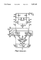
Referring to FIG. 2, which is a schematic diagram of a circuit in accordance with the invention, a pair of differential input signals are summed to produce a single differential output. Where the various circuit components function as they do in FIG. 1, the same designations are used. One of the major differences is that circuit nodes 23 and 24, which represent the input summing terminals of the output stage, comprise the nodes where the two input stages are coupled together indirectly rather than directly connected as in FIG. 1. In FIG. 2, the summing of the two input stages is accomplished by means of a pair of emitter-follower buffers. Thus, while coupled in common to the output stage, there is no direct connection to both input stages.
Emitter follower transistor 46, couples the collector of transistor 37 to node 23, which is directly connected to the collector of transistor 25. Thus, I1 flows out of node 23 into transistor 25. A second quantity of I1 flows through diode 21 into transistor 37. As a result, transistor 46 buffers transistor 37 from node 23 while providing the desired coupling.
Likewise, transistor 45 buffers transistor 38 from node 24 while providing the desired coupling. I1 flows out of node 24 into transistor 26. A similar quantity, I1, flows through diode 22 into transistor 38. It can be seen that diode 19 passes 4 I1. It is also to be noted that nodes 23 and 24 both operate at a potential of three diodes below VCC as does the circuit of FIG. 1.
As a result of the buffering action of transistors 44 and 45, nodes 23 and 24 are not commonly connected to the two input stages. The transconductance of the circuit is:
g.sub.m =I.sub.TOP /I.sub.1 *RE
It will be noted that the transconductance is double that of the circuit of FIG. 1. While this is not a spectacular improvement, it can be significant. In the proposed tunable filter application employing an integrated circuit the filter can employ a large number of cascaded filter stages. For example, in a typical product as many as eight FIG. 2 circuits can exist on a single chip. If the FIG. 1 approach were to be employed, twice the operating current, in transistors 14 and 15 (i.e., TOP), would be required to achieve the same transconductance as that of the invention shown in FIG. 2. This extra power dissipation is significant.
The invention has been described and a preferred embodiment detailed. When a person skilled in the art reads the foregoing description, alternatives and equivalents, within the spirit and intent of the invention, will be apparent. Accordingly, it is intended that the scope of the invention be limited only by the claims that follow.

Claims (6)

I claim:
1. A dual input signal summer circuit comprising:
an output stage that includes first and second differentially operated output stage bipolar transistors, the respective bases of the first and second output stage bipolar transistors being connected to first and second signal summing nodes;
a first input stage that includes first and second differentially operated first input stage bipolar transistors, the respective collectors of the first and second first input stage bipolar transistors being connected to the first and second signal summing nodes, the respective bases of the first and second first input stage bipolar transistors being connected to receive first and second signals of a first differential input signal;
a first emitter follower bipolar buffer transistor having a base, an emitter and a collector, the emitter of the first buffer transistor being connected to the first signal summing node;
a second emitter follower bipolar buffer transistor having a base, an emitter and a collector, the emitter of the second buffer transistor being connected to the second signal summing node; and
a second input stage that includes first and second differentially operated second input stage bipolar transistors, the respective bases of the first and second second input stage bipolar transistors being connected to receive first and second signals of a second differential input signal, the collector of the first second input stage bipolar transistor being connected to the base of the first buffer transistor, the collector of the second second input stage bipolar transistor being connected to the base of the second buffer transistor.
2. A dual input signal summer circuit as in claim 1 and further comprising:
a first constant current source connected between the collector of the first output stage bipolar transistor and a positive power supply, the collector of the first output stage bipolar transistor providing a first output signal of a differential output of the dual input signal summer circuit; and
a second constant current source connected between the collector of the second output stage bipolar transistor and the positive power supply, the collector of the second output stage bipolar transistor providing a second output signal of the differential output.
3. A dual input signal summer circuit as in claim 2 and wherein the emitters of the first and second output stage bipolar transistors are commonly connected to a negative supply voltage via a constant tail current element.
4. A dual input signal summer circuit as in claim 3 and further comprising:
a first diode string connected between the positive power supply and the first signal summing node; and
a second diode string connected between the positive power supply and the second signal summing node.
5. A dual input signal summer circuit as in claim 2 and wherein the first input stage further includes:
a first first stage Schottky diode connected between the base and the collector of the first first input stage bipolar transistor;
a second first stage Schottky diode connected between the base and the collector of the second first input stage bipolar transistor;
a first first stage constant current sink connected between the emitter of the first first input stage bipolar transistor and the negative power supply;
a second first stage constant current sink connected between the emitter of the second first input stage bipolar transistor and the negative power supply;
a first stage capacitor connected between the emitters of the first and second first input stage bipolar transistors; and
a first stage resistor connected between the emitters of the first and second first input stage bipolar transistors.
6. A dual input signal summer circuit as in claim 2 and wherein the second input stage further includes:
a first second stage Schottky diode connected between the base and the collector of the first second input stage bipolar transistor;
a second second stage Schottky diode connected between the base and the collector of the second second input stage bipolar transistor;
a first second stage constant current sink connected between the emitter of the first second input stage bipolar transistor and the negative power supply;
a second second stage constant current sink connected between the emitter of the second second input stage bipolar transistor and the negative power supply;
a second stage capacitor connected between the emitters of the first and second second input stage bipolar transistors; and
a second stage resistor connected between the emitters of the first and second second input stage bipolar transistor.
US07/926,594 1992-08-07 1992-08-07 Dual input signal summer circuit Expired - Lifetime US5357155A (en)

Priority Applications (3)

Application Number Priority Date Filing Date Title
US07/926,594 US5357155A (en) 1992-08-07 1992-08-07 Dual input signal summer circuit
EP93302344A EP0582365A1 (en) 1992-08-07 1993-03-26 Dual input signal summer circuit
JP5158524A JPH06103389A (en) 1992-08-07 1993-06-29 Adding circuit for double-input signal

Applications Claiming Priority (1)

Application Number Priority Date Filing Date Title
US07/926,594 US5357155A (en) 1992-08-07 1992-08-07 Dual input signal summer circuit

Publications (1)

Publication Number Publication Date
US5357155A true US5357155A (en) 1994-10-18

Family

ID=25453411

Family Applications (1)

Application Number Title Priority Date Filing Date
US07/926,594 Expired - Lifetime US5357155A (en) 1992-08-07 1992-08-07 Dual input signal summer circuit

Country Status (3)

Country Link
US (1) US5357155A (en)
EP (1) EP0582365A1 (en)
JP (1) JPH06103389A (en)

Cited By (3)

* Cited by examiner, † Cited by third party
Publication number Priority date Publication date Assignee Title
US5717350A (en) * 1994-11-09 1998-02-10 Micro Linear Corporation Degenerated differential pair waveform builder
US5913181A (en) * 1995-06-30 1999-06-15 Dallas Semiconductor Corp. Circuit for providing a switch signal to trigger changer in a digital potentiometer
US20090080309A1 (en) * 2005-05-18 2009-03-26 Rohm Co., Ltd. Arithmetic Processing Circuit Unit and Disc Device

Families Citing this family (1)

* Cited by examiner, † Cited by third party
Publication number Priority date Publication date Assignee Title
EP0846369A1 (en) * 1996-06-21 1998-06-10 Koninklijke Philips Electronics N.V. Variable-gain amplifier with pseudo-logarithmic gain control

Citations (4)

* Cited by examiner, † Cited by third party
Publication number Priority date Publication date Assignee Title
US4429416A (en) * 1982-03-26 1984-01-31 National Semiconductor Corporation Multistage cascade/cascode limiting IF amplifier and meter circuit
US4442549A (en) * 1982-05-27 1984-04-10 Motorola, Inc. Meter drive circuit
US4546275A (en) * 1983-06-02 1985-10-08 Georgia Tech Research Institute Quarter-square analog four-quadrant multiplier using MOS integrated circuit technology
US5057717A (en) * 1990-02-01 1991-10-15 Nec Corporation Logarithmic amplifier circuit

Patent Citations (4)

* Cited by examiner, † Cited by third party
Publication number Priority date Publication date Assignee Title
US4429416A (en) * 1982-03-26 1984-01-31 National Semiconductor Corporation Multistage cascade/cascode limiting IF amplifier and meter circuit
US4442549A (en) * 1982-05-27 1984-04-10 Motorola, Inc. Meter drive circuit
US4546275A (en) * 1983-06-02 1985-10-08 Georgia Tech Research Institute Quarter-square analog four-quadrant multiplier using MOS integrated circuit technology
US5057717A (en) * 1990-02-01 1991-10-15 Nec Corporation Logarithmic amplifier circuit

Non-Patent Citations (2)

* Cited by examiner, † Cited by third party
Title
M. J. Zuber et al., "A Wide-Bandwidth, High Accuracy Logarithmic Amplifier for Line-Scan Imaging Systems," Proceedings of the IEEE 1987 Custom Integrated Circuits Conference, May 4-7, 1987.
M. J. Zuber et al., A Wide Bandwidth, High Accuracy Logarithmic Amplifier for Line Scan Imaging Systems, Proceedings of the IEEE 1987 Custom Integrated Circuits Conference, May 4 7, 1987. *

Cited By (4)

* Cited by examiner, † Cited by third party
Publication number Priority date Publication date Assignee Title
US5717350A (en) * 1994-11-09 1998-02-10 Micro Linear Corporation Degenerated differential pair waveform builder
US5913181A (en) * 1995-06-30 1999-06-15 Dallas Semiconductor Corp. Circuit for providing a switch signal to trigger changer in a digital potentiometer
US20090080309A1 (en) * 2005-05-18 2009-03-26 Rohm Co., Ltd. Arithmetic Processing Circuit Unit and Disc Device
US7791989B2 (en) 2005-05-18 2010-09-07 Rohm Co., Ltd. Arithmetic processing circuit unit and disc device

Also Published As

Publication number Publication date
EP0582365A1 (en) 1994-02-09
JPH06103389A (en) 1994-04-15

Similar Documents

Publication Publication Date Title
EP0600852B1 (en) Logic circuit arrangements
JPH0775289B2 (en) Transconductance amplifier circuit
US3392342A (en) Transistor amplifier with gain stability
KR890001892B1 (en) Voltage addition circuit
GB1322516A (en) Signal translating stage
US3534279A (en) High current transistor amplifier stage operable with low current biasing
US3999139A (en) Monolithic alternately stacked IF amplifier
EP0114731A1 (en) Differential amplifier with high common-mode rejection
US4587491A (en) IC class AB amplifier output stage
US5357155A (en) Dual input signal summer circuit
EP0475507B1 (en) Amplifier arrangement
JPS61214807A (en) Amplification circuit
KR940001817B1 (en) Voltage-current transformation circuit for active filter
US5999050A (en) Differential amplifier, an integrated circuit, and a telephone
US4425551A (en) Differential amplifier stage having bias compensating means
US6734720B2 (en) Operational amplifier in which the idle current of its output push-pull transistors is substantially zero
US6278299B1 (en) Voltage to current converter
US3371286A (en) Stabilized direct-coupled push-pull amplifier
US4553107A (en) Current mirror circuit having stabilized output current
US4524330A (en) Bipolar circuit for amplifying differential signal
JP2569497B2 (en) Multiplier
US5525924A (en) Log conversion circuit
JPH0527282B2 (en)
JP3548127B2 (en) Low supply voltage analog multiplier
JPH0239881B2 (en)

Legal Events

Date Code Title Description
AS Assignment

Owner name: NATIONAL SEMICONDUCTOR CORPORATION A CORP. OF DE,

Free format text: ASSIGNMENT OF ASSIGNORS INTEREST.;ASSIGNOR:WILE, DONALD T.;REEL/FRAME:006185/0621

Effective date: 19920805

Owner name: NATIONAL SEMICONDUCTOR CORPORATION,CALIFORNIA

Free format text: ASSIGNMENT OF ASSIGNORS INTEREST;ASSIGNOR:WILE, DONALD T.;REEL/FRAME:006185/0621

Effective date: 19920805

STCF Information on status: patent grant

Free format text: PATENTED CASE

FEPP Fee payment procedure

Free format text: PAYOR NUMBER ASSIGNED (ORIGINAL EVENT CODE: ASPN); ENTITY STATUS OF PATENT OWNER: LARGE ENTITY

FPAY Fee payment

Year of fee payment: 4

FPAY Fee payment

Year of fee payment: 8

REMI Maintenance fee reminder mailed
FPAY Fee payment

Year of fee payment: 12