US5352943A - ECL to GaAs logic level shift interface circuit - Google Patents
ECL to GaAs logic level shift interface circuit Download PDFInfo
- Publication number
- US5352943A US5352943A US08/013,641 US1364193A US5352943A US 5352943 A US5352943 A US 5352943A US 1364193 A US1364193 A US 1364193A US 5352943 A US5352943 A US 5352943A
- Authority
- US
- United States
- Prior art keywords
- circuit
- power source
- output
- source voltage
- level
- Prior art date
- Legal status (The legal status is an assumption and is not a legal conclusion. Google has not performed a legal analysis and makes no representation as to the accuracy of the status listed.)
- Expired - Lifetime
Links
Images


Classifications
-
- H—ELECTRICITY
- H03—ELECTRONIC CIRCUITRY
- H03K—PULSE TECHNIQUE
- H03K19/00—Logic circuits, i.e. having at least two inputs acting on one output; Inverting circuits
- H03K19/0175—Coupling arrangements; Interface arrangements
- H03K19/0185—Coupling arrangements; Interface arrangements using field effect transistors only
- H03K19/018507—Interface arrangements
- H03K19/018535—Interface arrangements of Schottky barrier type [MESFET]
- H03K19/018542—Interface arrangements of Schottky barrier type [MESFET] with at least one differential stage
Definitions
- the present invention generally relates to compound semiconductor integrated circuits, and more particularly to a compound semiconductor integrated circuit such as a gallium arsenide (GaAs) integrated circuit having a built-in input interface circuit for converting an incoming logic signal of an emitter-coupled logic (ECL) level into a logic signal of a GaAs level which is used in an internal circuit which is provided at a stage subsequent to the interface circuit.
- GaAs gallium arsenide
- GaAs integrated circuits Recently, the integration density of GaAs integrated circuits has increased considerably, and thus, the GaAs integrated circuits are popularly used in applications where high speed operation and low power consumption are demanded. In such cases, there is a demand to use the GaAs integrated circuit together with the conventional ECL integrated circuit.
- an input interface circuit for converting the logic signal of the ECL level into the logic signal of the GaAs level is provided at the input part of the GaAs integrated circuit.
- FIG. 1 shows an essential part of an example of a conventional GaAs integrated circuit having a built-in input interface circuit for converting an input logic signal of the ECL level into a logic signal of the GaAs level.
- a logic signal SA having the ECL level that is, a high level of -1.14 [V] and a low level of -1.52 [V], for example, is input to an input terminal 1.
- An input interface circuit 2 converts the logic signal SA of the ECL level into complementary logic signals SC and SC having the GaAs level, that is, a high level of -0.45 [V] and a low level of -1.25 [V], for example.
- An internal circuit 3 is provided at a stage subsequent to the input interface circuit 2.
- This internal circuit 3 includes a positive phase input terminal 3A and an inverted phase input terminal 3B.
- An input part which is coupled to the positive and negative phase input terminals 3A and 3B has a threshold voltage of -0.8 [V] on the high level side and -0.9 [V] on the low level side, for example.
- a power line 4 is set to a ground voltage GND, and a power line 5 supplies a power source voltage V SS1 which is lower than the ground voltage GND.
- the power source voltage V SS1 is -1.25 [V].
- the internal circuit 3 operates using the ground voltage GND as the power source voltage on the high voltage side, and using the power source voltage V SS1 as the power source voltage on the low voltage side.
- a differential amplifier circuit 6 forms an input buffer.
- Power lines 7 and 8 are set to the ground voltage GND.
- a power line 9 supplies a power source voltage VS SS2 which is lower than the power source voltage V SS1 .
- the power source voltage V SS2 is -2.0 [V].
- the power source voltage V SS1 which is smaller in absolute value compared to the power source voltage V SS2 is used to drive the internal circuit 3.
- the power source voltages V SS1 and V SS2 are supplied from independent power sources.
- Enhancement type Schottky gate field effect transistors (hereinafter simply referred to as E-FETs) 10 and 11 are provided as driving transistors.
- a reference voltage V ref is applied to a reference voltage input terminal 12 and is supplied to E-FET 11.
- the reference voltage V ref is -1.33 [V].
- a depletion type Schottky gate field effect transistor (hereinafter simply referred to as D-FET) 13 forms a current source.
- the D-FETs 14 and 15 are used as loads.
- the circuit constants of the differential amplifier circuit 6 are set so that the high level threshold voltage is -0.9 [V] and the low level threshold voltage is -1.9 [V], for example, and outputs a positive phase logic signal SB via a node 16 and an inverted phase logic signal SB via a node 17.
- the positive and inverted phase logic signals SB and SB have a high level of 0 [V] and a low level of -1.0 [V].
- a level conversion circuit 18 converts the positive phase logic signal SB output from the differential amplifier circuit 6 into the positive phase logic signal SC having the GaAs level.
- This level conversion circuit 18 includes an E-FET 21 connected to a power line 19 which is set to the ground voltage GND, a diode 22, and a D-FET 23 connected to a power line 20 which supplies the power source voltage V SS2 .
- the positive phase logic signal SC of the GaAs level is output via a node 24.
- the circuit constants of the level conversion circuit 18 are set so that the level conversion circuit 18 outputs -0.45 [V], for example, which is the high level of the GaAs level when the E-FET 21 is ON and outputs -1.25 [V], for example, which is the low level of the GaAs level when the E-FET 21 is OFF.
- a level conversion circuit 25 converts the inverted phase logic signal SB which is output from the differential amplifier circuit 6 into the inverted phase logic signal SC of the GaAs level.
- This level conversion circuit 25 includes an E-FET 28 connected to a power line 26 which is set to the ground voltage GND, a diode 29, and a D-FET 30 which is connected to a power line 27 which supplies the power source voltage V SS2 .
- the inverted phase logic signal SC of the GaAs level is output via a node 31.
- the circuit constants of the level conversion circuit 25 are set so that the level conversion circuit 25 outputs -0.45 [V], for example, which is the high level of the GaAs level when the E-FET 28 is ON and outputs -1.25 [V], for example, which is the low level of the GaAs level when the E-FET 28 is OFF.
- the logic signal SA of the ECL level input to the input terminal 1 has the high level
- the E-FET 10 of the differential amplifier circuit 6 turns ON and the E-FET 11 of the differential amplifier circuit 6 turns OFF.
- the positive and negative phase signals SB and SB output from the differential amplifier circuit 6 respectively have the high level and the low level.
- the E-FET 21 of the level conversion circuit 18 turns ON, and a signal having the high level of the GaAs level is output via the node 24.
- This signal output via the node 24 is supplied to the positive phase input terminal 3A of the internal circuit 3.
- the E-FET 28 of the level conversion circuit 25 turns OFF, and a signal having the low level of the GaAs level is output via the node 31.
- This signal output via the node 31 is supplied to the inverted phase input terminal 3B of the internal circuit 3.
- the logic signal SA of the ECL level input to the input terminal 1 has the low level
- the E-FETs 10 and 11 of the differential amplifier circuit 6 respectively turn OFF and ON.
- the positive phase logic signal SB and the inverted phase logic signal SB output from the differential amplifier circuit 6 respectively have the low level and the high level.
- the E-FET 21 of the level conversion circuit 18 turns OFF, and a signal having the low level of the GaAs level is output via the node 31.
- This signal output via the node 31 is supplied to the inverted phase input terminal 3B of the internal circuit 3.
- the input interface circuit 2 and the internal circuit 3 use mutually different power source voltages on the low voltage side. For this reason, if the power source voltage V SS1 undergoes an absolute or relative deviation with respect to the power source voltage V SS2 , the threshold voltages of the input part of the internal circuit 3 undergo an absolute or relative deviation with respect to the logic signals SC and SC which are output from the interface circuit 2. If the threshold voltages of the input part of the internal circuit 3 undergo an absolute or relative deviation with respect to the logic signals SC and SC, the logic signals SC and SC output from the input interface circuit 2 cannot be transferred correctly to the internal circuit 3, and there is a problem in that an erroneous operation is generated.
- FIG. 2 is a diagram for explaining the deviation of the threshold voltages of the input part of the internal circuit 3.
- FIG. 2(a) shows the high level and the low level of the logic signals SC and SC which are output from the input interface circuit 2, where VOH and VOL respectively denote the high level and the low level.
- FIG. 2(b) shows the threshold voltages of the input part of the internal circuit 3 for the case where the power source voltage V SS1 undergoes no absolute or relative deviation with respect to the power source voltage V SS2 , where VIH and VIL respectively denote the high level and the low level of the threshold voltages.
- VIH and VIL respectively denote the high level and the low level of the threshold voltages.
- VOH>VIH and VOL ⁇ VIL the input part of the internal circuit 3 can accurately judge the high and low levels of the signals output from the input interface circuit 2.
- FIG. 2(c) shows an example of a deviation in the threshold voltages of the input part of the internal circuit 3 for the case where the power source voltage V SS1 undergoes an absolute or relative deviation in the negative direction with respect to the power source voltage V SS2 , where VIH' and VIL' respectively denote the threshold voltages for the high level and the low level. Since VOL>VIL' in this case, the input part of the internal circuit 3 cannot judge the low level of the signals which are output from the input interface circuit 2.
- FIG. 2(d) shows an example of a deviation in the threshold voltages of the input part of the internal circuit 3 for the case where the power source voltage V SS1 undergoes an absolute or relative deviation in the positive direction with respect to the power source voltage V SS2 , where VIH" and VIL" respectively denote the threshold voltages for the high level and the low level. Since VOH ⁇ VIH" in this case, the input part of the internal circuit 3 cannot judge the high level of the signals which are output from the input interface circuit 2.
- Another and more specific object of the present invention is to provide a compound semiconductor integrated circuit adapted to provide an interface with respect to an internal circuit which is driven by first and second power source voltages and operates responsive to a logic signal having a predetermined logic level which is different from an emitter-coupled logic level, comprising an input terminal for receiving an input logic signal having the emitter-coupled logic level, input circuit means, coupled to the input terminal and driven by the first and third power source voltages, for receiving the input logic signal via the input terminal, and output circuit means, coupled to the input circuit means and driven by the first and second power source voltages, for converting an output signal of the input circuit means into a signal having the predetermined logic level, where the second power source voltage is lower than the first power source voltage, the third power source voltage is different from the second power source voltage and is lower than the first power source voltage, and the output circuit means supplies an output thereof to the internal circuit.
- the compound semiconductor integrated circuit of the present invention it is possible to correctly transfer the logic level of the input logic signal to the internal circuit even if a relative deviation occurs in a difference between the second and third power source voltages. As a result, it is possible to prevent an erroneous operation of the internal circuit.
- FIG. 1 is a circuit diagram showing an essential part of an example of a conventional GaAs integrated circuit
- FIG. 2 is a diagram for explaining a deviation in threshold voltages of an input part of an internal circuit shown in FIG. 1;
- FIG. 3 is a system block diagram for explaining the operating principle of the present invention.
- FIG. 4 is a circuit diagram showing an essential part of a first embodiment of a compound semiconductor integrated circuit according to the present invention.
- FIGS. 5 and 6 respectively are diagrams for explaining the relationship of high and low levels of logic signals output from an input interface circuit of the first embodiment and threshold voltages of an input part of an internal circuit of the first embodiment;
- FIG. 7 is a graph showing a power source voltage dependency of a positive phase logic signal output from the input interface circuit of the first embodiment
- FIG. 8 is a graph showing a power source voltage dependency of an inverted phase logic signal output fro the input interface circuit of the first embodiment
- FIG. 9 is a circuit diagram showing an essential part of a second embodiment of the compound semiconductor ingegrated circuit according to the present invention.
- FIG. 10 is a circuit diagram showing an equivalent circuit of the second embodiment for describing the operation thereof.
- FIG. 11 is a circuit diagram showing an equivalent logic circuit of the first embodiment
- FIG. 12 is a circuit diagram showing an equivalent circuit of the second embodiment
- FIG. 13 is a circuit diagram showing an essential part of a third embodiment of the compound semiconductor integrated circuit according to the present invention.
- FIG. 14 is a circuit diagram showing an essential part of a fourth embodiment of the compound semiconductor integrated circuit according to the present invention.
- FIG. 15 is a circuit diagram showing an essential part of a fifth embodiment of the compound semiconductor integrated circuit according to the present invention.
- FIGS. 16 and 17 respectively are graphs for explaining the power source voltage dependencies of positive and inverted phase logic signals output fro the input interface circuit of the fifth embodiment for different power source voltages V SS1 ;
- FIGS. 18 and 19 respectively are graphs for explaining the power source voltage dependencies of positive and inverted phase logic signals output from the input interface circuit of the fifth embodiment for different power source voltages V SS2 .
- an input interface circuit 34 includes an input circuit part 35 and an output circuit part 36. This input interface circuit 34 is coupled to an internal circuit 32.
- the internal circuit 32 operates with logic signals having levels different from the ECL level which is used in the input interface circuit 34.
- the input interface circuit 34 and the internal circuit 32 may be provided on a single semiconductor chip.
- the input and output circuit parts 35 and 36 of the input interface circuit 34 and the internal circuit 32 are coupled to a power line which supplies a power source voltage V1.
- the internal circuit 32 is also coupled to a power line which supplies a power source voltage V2 which is lower than the power source voltage V1.
- the power source voltage V1 is on the high voltage side
- the power source voltage V2 is on the low voltage side.
- the input circuit part 35 of the input interface circuit 34 is also coupled to a power line which supplies a power source voltage V3, and the output circuit part 36 of the input interface circuit 34 is also coupled to the power line which supplies the power source voltage V2.
- the input interface circuit 34 uses the power source voltage V1 as power source voltage on the high voltage side, and the power source voltage V3 which is lower than the power source voltage V1 as the power source voltage on the low voltage side.
- the input circuit part 35 of the input interface circuit 34 operates using the power source voltage V3 as the power source voltage on the low voltage side.
- the output circuit part of the input interface circuit 34 uses the power source voltage V1 as the power source voltage on the high voltage side and the power source voltage V2 as the power source voltage on the low voltage side, similarly as in the case of the internal circuit 32.
- FIGS. 4 through 9 those parts which are the same as those corresponding parts in FIG. 1 are designated by the same reference numerals, and a description thereof will be omitted.
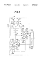
- FIG. 4 shows an essential part of the first embodiment.
- an input circuit part of an input interface circuit 37 includes a differential amplifier circuit 6, and level conversion circuits 18 and 25.
- An output circuit part of the input interface circuit 37 includes push-pull circuits 38 and 39.
- the push-pull circuits 38 and 39 are respectively connected between the level conversion circuit 18 and a positive phase input terminal 3A of an internal circuit 3 and between the level conversion circuit 25 and an inverted phase input terminal 3B of the internal circuit 3.
- this embodiment is constructed similarly to the conventional GaAs integrated circuit shown in FIG. 1.
- the push-pull circuit 38 outputs a positive phase logic signal SD of the GaAs level.
- a power line 40 is set to the ground voltage GND, and a power line 41 supplies the power source voltage V SS1 .
- the push-pull circuit 38 includes an E-FET 42 and a D-FET 43, and the drain of the E-FET 42 is connected to the power line 40 which is set to the ground voltage GND.
- the gate of the E-FET 42 is connected to a node 16 of the differential amplifier circuit 6.
- the D-FET 43 has its drain connected to the source of the E-FET 42, its gate connected to a node 31 of the level conversion circuit 25, and its source connected to the power line 41.
- a node 44 which connects the source of the E-FET 42 and the drain of the D-FET 43 is connected to the positive phase input terminal 3A of the internal circuit 3.
- the circuit constants of the push-pull circuit 38 are set so that a high level of the GaAs level, that is, -0.45 [V], for example, is output via the node 44 when the E-FET 42 and the D-FET 43 are respectively turned ON and OFF, and a low level of the GaAs level, that is, -1.25 [V], for example, is output via the node 44 when the E-FET 42 and the D-FET 43 are respectively turned OFF and ON.
- the push-pull circuit 39 outputs an inverted phase logic signal SD of the GaAs level.
- a power line 45 is set to the ground voltage GND, and a power line 46 supplies the power source voltage V SS1 .
- the push-pull circuit 39 includes an E-FET 47 and a D-FET 48, and the drain of the E-FET 47 is connected to the power line 45 which is set to the ground voltage GND.
- the gate of the E-FET 47 is connected to a node 17 of the differential amplifier circuit 6.
- the D-FET 48 has its drain connected to the source of the E-FET 47, its gate connected to a node 24 of the level conversion circuit 18, and its source connected to the power line 46.
- a node 49 which connects the source of the E-FET 47 and the drain of the D-FET 48 is connected to the inverted phase input terminal 3B of the internal circuit 3.
- the circuit constants of the push-pull circuit 39 are set so that a high level of the GaAs level, that is, -0.45 [V], for example, is output via the node 49 when the E-FET 47 and the D-FET 48 are respectively turned ON and OFF, and a low level of the GaAs level, that is, -1.25 [V], for example, is output via the node 49 when the E-FET 47 and the D-FET 48 are respectively turned OFF and ON.
- the E-FETs 10 and 11 of the differential amplifier circuit 6 respectively turn ON and OFF, and the positive and inverted phase output signals SB and SB respectively have the high level and the low level.
- the E-FET 21 of the level conversion circuit 18 turns ON, and a high-level signal having the voltage V SS1 , for example, is output via the node 24.
- the E-FET 28 of the level conversion circuit 25 turns OFF, and a low-level signal having the voltage V SS2 , for example, is output via the node 31.
- the E-FET 42 turns ON, the D-FET 43 turns OFF, and a high-level signal of the GaAs level is output via the node 44.
- the E-FET 47 turns OFF, the D-FET 48 turns ON, and a low-level signal of the GaAs level is output via the node 49.
- the logic signal SA of the ECL level input to the input terminal 1 has the low level
- the E-FETs 10 and 11 of the differential amplifier circuit 6 respectively turn OFF and ON
- the positive and inverted phase output signals SB and SB respectively have the low level and the high level.
- the E-FET 21 of the level conversion circuit 18 turns OFF, and a low-level signal having the voltage V SS2 , for example, is output via the node 24.
- the E-FET 28 of the level conversion circuit 25 turns ON, and a high-level signal having the voltage V SS1 , for example, is output via the node 31.
- the E-FET 42 turns OFF, the D-FET 43 turns ON, and a low-level signal of the GaAs level is output via the node 44.
- the E-FET 47 turns ON, the D-FET 48 turns OFF, and a high-level signal of the GaAs level is output via the node 49.
- the differential amplifier circuit 6 and the level conversion circuits 18 and 25 which form the input circuit part of the input interface circuit 37 are designed to operate using the ground voltage GND as the power source voltage on the high voltage side and the power source voltage V SS2 as the power source voltage on the low voltage side.
- the push-pull circuits 38 and 39 which form the output circuit part of the input interface circuit 37 are designed to operate using the ground voltage GND as the power source voltage on the high voltage side and the power source voltage V SS1 as the power source voltage on the low voltage side, similarly as in the case of the internal circuit 3.
- the power source voltage V SS1 undergoes an absolute or relative deviation in the negative direction with respect to the power source voltage V SS2 , the high-level voltage VOH and the low-level voltage VOL of the logic signals SD and SD output from the input interface circuit 37 and the threshold voltages VIH and VIL of the input part of the internal circuit 3 respectively shift in the negative direction as shown in FIG. 5.
- the high-level voltage VOH and the low-level voltage VOL of the logic signals SD and SD output from the input interface circuit 37 and the threshold voltages VIH and VIL of the input part of the internal circuit 3 respectively shift in the positive direction as shown in FIG. 6.
- FIG. 7 shows a simulation result of the amount of shift of the positive phase logic signal SD which is output from the input interface circuit 37 when the power source voltage V SS2 is -2.0 [V] and the power source voltage V SS1 deviates, where the abscissa indicates the voltage of the logic signal SA of the ECL level and the ordinate indicates the voltage of the logic signal SD.
- FIG. 8 shows a simulation result of the amount of shift of the inverted phase logic signal SD which is output from the input interface circuit 37 when the power source voltage V SS2 is -2.0 [V] and the power source voltage V SS1 deviates, where the abscissa indicates the voltage of the logic signal SA of the ECL level and the ordinate indicates the voltage of the logic signal SD.
- the logic signals SD and SD output from the input interface circuit 37 and the threshold voltages VIH and VIL of the input part of the internal circuit 3 in the same direction when the power source voltage V SS1 undergoes an absolute or relative deviation in the positive direction with respect to the power source voltage V SS2 .
- the logic signals SD and SD output from the input interface circuit 37 can be transferred correctly to the internal circuit 3. In other words, it is possible to positively avoid an erroneous operation which is caused by an incorrect transfer of the logic signals SD and SD to the internal circuit 3.
- FIG. 9 shows an essential part of the second embodiment
- FIG. 10 shows an equivalent circuit of an essential part of the second embodiment.
- those parts which are the same as those corresponding parts in FIG. 4 are designated by the same reference numerals, and a description thereof will be omitted.
- circuits 51 and 52 are provided as shown in FIG. 9 in place of the level conversion circuits 18 and 19 and the push-pull circuits 38 and 39.
- the circuit 51 includes E-FETs 54 and 55, and a D-FET 56.
- the circuit 52 includes E-FETs 57 and 58, and a D-FET 59.
- the differential amplifier circuit 6 forms an input circuit part of the input interface circuit 37
- the circuits 51 and 52 form an output circuit part of the input interface circuit 37.
- the logic signal SD is output from a node which connects the E-FET 55 and the D-FET 56
- the logic signal SD is output from a node which connects the E-FET 58 and the D-FET 59.
- the ground voltage GND is 0 [V]
- the power source voltage V SS1 is -1.6 [V]
- the power source voltage V SS2 is -2.0 [V].
- the D-FET 14 and the E-FET 57 form a level conversion circuit
- the D-FET 15 and the E-FET 54 form another level conversion circuit.
- the D-FET 14 and the E-FET 57 and the D-FET 15 and the E-FET 54 are respectively coupled to mutually different power source voltages V SS2 and V SS1
- the provision of the D-FET 13 which is used as a current source sets a node 60 to a kind of a floating state when the level conversion takes place. That is, the node 60 is maintained to an intermediate level weven if the power source voltage V SS1 (or V SS2 ) deviates.
- the logic signal SD takes a high level (for example, approximately -0.9 [V]) in response to the high level (for example, approximately 0 to -0.5 [V]) of the logic signal SD.
- the E-FET 57 turns ON resposive to the high-level logic signal SD, and the logic signal SB is pulled towards the low level. Accordingly, the transition of the logic signal SB to the high level is accelerated by the low-level logic signal SB.
- the logic signal SA which is applied to the input terminal 1 controls the logic signals SB and SB.
- a push-pull circuit means including the E-FETs 54 and 57 accelerates the changes when the logic signals SB and SB are controlled.
- the logic signal SB takes a low level as is clear from the logic circuit of the second embodiment shown in FIG. 12.
- the source potential of the E-FET 11 which receives the reference voltage V ref via the input terminal 12 rises due to the operation of the current source formed by the D-FET 13, and the E-FET 11 turns OFF as a result.
- the logic signal SA changes from the low level to the high level, it appears within the input interface circuit 37 as if the reference voltage V ref changed from the high level to the low level, because the E-FET 11 turns OFF.
- the actual reference voltage V ref is fixed and does not change.
- Each circuit part surrounded by a dotted line in FIG. 10 functions as a 2-input NOR circuit which is coupled to a source follower, and also functions as a level conversion circuit which carries out a level conversion between the power source voltages V SS1 and V SS2 .
- the source follower is formed by the E-FET 58 and the D-FET 59 which may be considered as a buffer circuit.
- each D-FET which functions as a current source is indicated as a current source.
- an equivalent logic circuit of this embodiment becomes as shown in FIG. 12 compared to an equivalent logic circuit of the first embodiment shown in FIG. 11.
- the first embodiment is suited for use in a memory such as a RAM, and basically comprises inverters and buffers INV1 through INV4 which are connected as shown in FIG. 11.
- the second embodiment is suited for use in a register or a latch circuit, and basically comprises two 2-input NOR circuits NOR1 and NOR2. Hence, the second embodiment enables a more easier circuit control compared to the first embodiment.
- FIG. 13 a description will be given of a third embodiment of the compound semiconductor integrated circuit according to the present invention, by referring to FIG. 13.
- those parts which are the same as those corresponding parts in FIG. 9 are designated by the same reference numerals, and a description thereof will be omitted.
- a circuit 52A includes the E-FET 57, E-FETs 58 1 through 58 3 , and D-FETs 59 1 through 59 3 .
- the circuits 51 and 52A form the output circuit part of the input interface circuit 37.
- the logic signal SD1 is output from a node which connects the E-FET 58 3 and the D-FET 59 3
- the logic signal SD2 is output from a node which connects the E-FET 58 2 and the D-FET 59 2 .
- this embodiment Compared to the second embodiment which outputs the complementary logic signals SD and SD, this embodiment outputs logic signals SD1 and SD2. In other wods, the second embodiment outputs an OR output and a NOR output. On the other hand, this embodiment outputs two OR outputs.
- FIG. 14 a description will be given of a fourth embodiment of the compound semiconductor integrated circuit according to the present invention, by referring to FIG. 14.
- those parts which are the same as those corresponding parts in FIGS. 9 and 13 are designated by the same reference numerals, and a description thereof will be omtited.
- a circuit 51B includes the E-FET 54, E-FETs 55 1 and 55 2 , and D-FETs 56 1 and 56 2 .
- a circuit 52B includes the E-FET 57, E-FETs 58 1 and 58 2 , and D-FETs 59 1 and 59 2 .
- the circuits 51B and 52B form the output circuit part of the input interface circuit 37.
- the logic signal SD is output from a node which connects the E-FET 55 2 and the D-FET 56 2
- the logic signal SD is output from a node which connects the E-FET 58 2 and the D-FET 59 2 .
- the large capacitance affects the signal at the inverted phase input terminal 3B of the internal circuit 3.
- a mutual interference occurs between the logic signals SD and SD.
- This mutual interference occurs because the gate of the E-FET 57 of the circuit 52 which outputs the logic signal SD is connected to the output of the circuit 51, that is, the node which connects the E-FET 55 and the D-FET 56 and outputs the logic signal SD.
- a waveform distortion of the logic signal SD caused by the large capacitance connected to the positive phase input terminal 3A causes an inevitable delay in the operation of the circuit 52, thereby introducing the mutual interference.
- this fourth embodiment shown in FIG. 14 is designed to eliminate the above described mutual interference.
- the source followers are provided in two stages in each of the circuits 51B and 52B, so as to minimize the effects on each other.
- the input circuit part of the input interface circuit is made up of a single stage, but it is possible to provide two or more stages of circuits if the gain obtainable by a single stage is insufficient.
- FIG. 15 shows an essential part of a fifth embodiment of the compound semiconductor integrated circuit according to the present invention, in which the input circuit part of the input interface circuit is made up of two stages.
- FIG. 15 shows the two-stage construction applied to the second embodiment, but the two-stage construction is similarly applicable to any of the first through fourth embodiments.
- those parts which are the same as those corresponding parts in FIG. 9 are designated by the same reference numerals, and a description thereof will be omitted.
- first and second stages ST1 and ST2 of the input circuit part of the input interface circuit 37 have basically the same construction, and thus, a description will only be given of the second stage ST2 of the input circuit part.
- GND 0 [V]
- V SS1 -1.6 [V]
- V SS2 -2.0 [V].
- the reference voltage V ref is -1.33 [V]
- a reference voltage V CL is -1.0 [V].
- level conversion circuits 71 and 72 are provided to match the signal levels in the second stage ST2 with the signal elvels of the first stage ST1, and the first stage ST1 also includes similar level conversion circuits for the same purpose.
- the level conversion circuits 71 and 72 respectively include D-FETs 75 and 76, and a diode 77.
- the stage ST2 further includes a clamp circuit 81 which includes E-FETs 83 and 84.
- the reference voltage V CL is applied to the clamp circuit 81 to clamp the low level in a vicinity of -1.0 [V], so as to reduce the signal amplitude to a minimum amplitude which guarantees correct circuit operation and prevents deterioration of the circuit operation speed.
- the clamp circuits 81 in the first and second stages ST1 and ST2 also function to average and stabilize the signal levels output from the first and second stages ST1 and ST2.
- FIGS. 16 and 17 respectively show simulation results for explaining the power source voltage dependencies of positive and inverted phase logic signals SD ad SD outout from the input interface circuit 37 of the fifth embodiment for different power source voltages V SS1 .
- the simulation results shown in FIGS. 16 and 17 are obtained for the power source voltage V SS2 of -1.8 [V].
- FIGS. 18 and 19 respectively show simulation results for explaining the power source voltage dependencies of positive and inverted phase logic signals SD and SD output from the input interface circuit 37 of the fifth embodiment for different power source voltages V SS1 .
- the simulation results shown in FIGS. 18 and 19 are obtained for the power source voltage V SS1 of -1.6 [V].
Landscapes
- Engineering & Computer Science (AREA)
- Computer Hardware Design (AREA)
- Physics & Mathematics (AREA)
- Computing Systems (AREA)
- General Engineering & Computer Science (AREA)
- Mathematical Physics (AREA)
- Logic Circuits (AREA)
Abstract
Description
Claims (12)
Applications Claiming Priority (4)
| Application Number | Priority Date | Filing Date | Title |
|---|---|---|---|
| JP4-021310 | 1992-02-06 | ||
| JP2131092 | 1992-02-06 | ||
| JP5016074A JPH05284004A (en) | 1992-02-06 | 1993-02-03 | Compound semiconductor integrated circuit |
| JP5-016074 | 1993-02-03 |
Publications (1)
| Publication Number | Publication Date |
|---|---|
| US5352943A true US5352943A (en) | 1994-10-04 |
Family
ID=26352321
Family Applications (1)
| Application Number | Title | Priority Date | Filing Date |
|---|---|---|---|
| US08/013,641 Expired - Lifetime US5352943A (en) | 1992-02-06 | 1993-02-04 | ECL to GaAs logic level shift interface circuit |
Country Status (1)
| Country | Link |
|---|---|
| US (1) | US5352943A (en) |
Cited By (2)
| Publication number | Priority date | Publication date | Assignee | Title |
|---|---|---|---|---|
| US20050146493A1 (en) * | 2000-12-07 | 2005-07-07 | Arata Kinjo | Semiconductor integrated circuit, liquid crystal drive device, and liquid crystal display system |
| US20050190691A1 (en) * | 2004-02-27 | 2005-09-01 | Toshiki Seshita | High-frequency switch apparatus |
Citations (4)
| Publication number | Priority date | Publication date | Assignee | Title |
|---|---|---|---|---|
| US4789798A (en) * | 1985-10-07 | 1988-12-06 | Gould Inc. | ECL to GaaS logic conversion circuit with positive feedback |
| US5021691A (en) * | 1988-06-27 | 1991-06-04 | Nec Corporation | Level conversion circuit having capability of supplying output signal with controlled logical level |
| US5159208A (en) * | 1990-03-20 | 1992-10-27 | Fujitsu Limited | Interface circuit provided between a compound semiconductor logic circuit and a bipolar transistor circuit |
| US5248909A (en) * | 1990-01-09 | 1993-09-28 | Fujitsu Limited | ECL-TO-GaAs level converting circuit |
-
1993
- 1993-02-04 US US08/013,641 patent/US5352943A/en not_active Expired - Lifetime
Patent Citations (4)
| Publication number | Priority date | Publication date | Assignee | Title |
|---|---|---|---|---|
| US4789798A (en) * | 1985-10-07 | 1988-12-06 | Gould Inc. | ECL to GaaS logic conversion circuit with positive feedback |
| US5021691A (en) * | 1988-06-27 | 1991-06-04 | Nec Corporation | Level conversion circuit having capability of supplying output signal with controlled logical level |
| US5248909A (en) * | 1990-01-09 | 1993-09-28 | Fujitsu Limited | ECL-TO-GaAs level converting circuit |
| US5159208A (en) * | 1990-03-20 | 1992-10-27 | Fujitsu Limited | Interface circuit provided between a compound semiconductor logic circuit and a bipolar transistor circuit |
Cited By (7)
| Publication number | Priority date | Publication date | Assignee | Title |
|---|---|---|---|---|
| US20050146493A1 (en) * | 2000-12-07 | 2005-07-07 | Arata Kinjo | Semiconductor integrated circuit, liquid crystal drive device, and liquid crystal display system |
| US20070279357A1 (en) * | 2000-12-07 | 2007-12-06 | Arata Kinjo | Semiconductor integrated circuit, liquid crystal drive device, and liquid crystal display system |
| US20070279358A1 (en) * | 2000-12-07 | 2007-12-06 | Arata Kinjo | Semiconductor integrated circuit, liquid crystal drive device, and liquid crystal display system |
| US20070279404A1 (en) * | 2000-12-07 | 2007-12-06 | Arata Kinjo | Semiconductor integrated circuit, liquid crystal drive device, and liquid crystal display system |
| US7405732B2 (en) | 2000-12-07 | 2008-07-29 | Renesas Technology Corp. | Semiconductor integrated circuit, liquid crystal drive device, and liquid crystal display system |
| US8094104B2 (en) | 2000-12-07 | 2012-01-10 | Hitachi Ulsi Systems Co., Ltd. | Semiconductor integrated circuit, liquid crystal drive device, and liquid crystal display system |
| US20050190691A1 (en) * | 2004-02-27 | 2005-09-01 | Toshiki Seshita | High-frequency switch apparatus |
Similar Documents
| Publication | Publication Date | Title |
|---|---|---|
| EP0886379B1 (en) | Voltage-level shifter | |
| US5381061A (en) | Overvoltage tolerant output buffer circuit | |
| US6255888B1 (en) | Level shift circuit | |
| US6801064B1 (en) | Buffer circuit using low voltage transistors and level shifters | |
| EP1229650B1 (en) | Output circuit, input circuit and input/output circuit | |
| US5075581A (en) | Ecl to ttl voltage level converter using cmos and bicmos circuitry | |
| US5036226A (en) | Signal converting circuit | |
| JP2516302B2 (en) | Differential receiver | |
| US20030146781A1 (en) | High speed voltage level shifter | |
| US5929679A (en) | Voltage monitoring circuit capable of reducing power dissipation | |
| US6650167B1 (en) | Multi-level/single ended input level shifter circuit | |
| US20040217798A1 (en) | Level shifter circuit | |
| US5880617A (en) | Level conversion circuit and semiconductor integrated circuit | |
| US5592108A (en) | Interface circuit adapted for connection to following circuit using metal-semiconductor type transistor | |
| US20230238946A1 (en) | Level shifter | |
| US4890051A (en) | CMOS input buffer stable for the variation of a power supplying voltage | |
| US10644691B2 (en) | Semiconductor integrated circuit | |
| EP0762648B1 (en) | Bus hold circuit | |
| US5352943A (en) | ECL to GaAs logic level shift interface circuit | |
| US5276366A (en) | Digital voltage level translator circuit | |
| US12334920B2 (en) | Level shifter | |
| US5332936A (en) | Composite logic circuit | |
| US5159208A (en) | Interface circuit provided between a compound semiconductor logic circuit and a bipolar transistor circuit | |
| EP0632596B1 (en) | Logic gate circuit formed of semiconductor transistors | |
| EP0388074A1 (en) | Cmos level shifting circuit |
Legal Events
| Date | Code | Title | Description |
|---|---|---|---|
| AS | Assignment |
Owner name: FUJITSU QUANTUM DEVICES LIMITED, JAPAN Free format text: ASSIGNMENT OF ASSIGNORS INTEREST;ASSIGNORS:TSUKAHARA, KAZUHISA;KANEKO, YOSHIAKI;KOYANAGI, MAYA;REEL/FRAME:006525/0888 Effective date: 19930325 Owner name: FUJITSU LIMITED, JAPAN Free format text: ASSIGNMENT OF ASSIGNORS INTEREST;ASSIGNORS:TSUKAHARA, KAZUHISA;KANEKO, YOSHIAKI;KOYANAGI, MAYA;REEL/FRAME:006525/0888 Effective date: 19930325 |
|
| STCF | Information on status: patent grant |
Free format text: PATENTED CASE |
|
| FEPP | Fee payment procedure |
Free format text: PAYOR NUMBER ASSIGNED (ORIGINAL EVENT CODE: ASPN); ENTITY STATUS OF PATENT OWNER: LARGE ENTITY |
|
| FPAY | Fee payment |
Year of fee payment: 4 |
|
| FPAY | Fee payment |
Year of fee payment: 8 |
|
| FPAY | Fee payment |
Year of fee payment: 12 |
|
| AS | Assignment |
Owner name: FUJITSU MICROELECTRONICS LIMITED, JAPAN Free format text: ASSIGNMENT OF ASSIGNORS INTEREST;ASSIGNOR:FUJITSU LIMITED;REEL/FRAME:022309/0544 Effective date: 20090123 Owner name: FUJITSU MICROELECTRONICS LIMITED,JAPAN Free format text: ASSIGNMENT OF ASSIGNORS INTEREST;ASSIGNOR:FUJITSU LIMITED;REEL/FRAME:022309/0544 Effective date: 20090123 |
|
| AS | Assignment |
Owner name: FUJITSU SEMICONDUCTOR LIMITED, JAPAN Free format text: CHANGE OF NAME;ASSIGNOR:FUJITSU MICROELECTRONICS LIMITED;REEL/FRAME:024982/0245 Effective date: 20100401 |