US5313066A - Electronic method and apparatus for acquiring an X-ray image - Google Patents
Electronic method and apparatus for acquiring an X-ray image Download PDFInfo
- Publication number
- US5313066A US5313066A US08/044,427 US4442793A US5313066A US 5313066 A US5313066 A US 5313066A US 4442793 A US4442793 A US 4442793A US 5313066 A US5313066 A US 5313066A
- Authority
- US
- United States
- Prior art keywords
- microplates
- lines
- conductive
- address
- layer
- Prior art date
- Legal status (The legal status is an assumption and is not a legal conclusion. Google has not performed a legal analysis and makes no representation as to the accuracy of the status listed.)
- Expired - Fee Related
Links
Images


Classifications
-
- H—ELECTRICITY
- H10—SEMICONDUCTOR DEVICES; ELECTRIC SOLID-STATE DEVICES NOT OTHERWISE PROVIDED FOR
- H10F—INORGANIC SEMICONDUCTOR DEVICES SENSITIVE TO INFRARED RADIATION, LIGHT, ELECTROMAGNETIC RADIATION OF SHORTER WAVELENGTH OR CORPUSCULAR RADIATION
- H10F39/00—Integrated devices, or assemblies of multiple devices, comprising at least one element covered by group H10F30/00, e.g. radiation detectors comprising photodiode arrays
- H10F39/10—Integrated devices
- H10F39/12—Image sensors
- H10F39/191—Photoconductor image sensors
-
- G—PHYSICS
- G01—MEASURING; TESTING
- G01T—MEASUREMENT OF NUCLEAR OR X-RADIATION
- G01T1/00—Measuring X-radiation, gamma radiation, corpuscular radiation, or cosmic radiation
- G01T1/16—Measuring radiation intensity
- G01T1/24—Measuring radiation intensity with semiconductor detectors
- G01T1/241—Electrode arrangements, e.g. continuous or parallel strips or the like
-
- G—PHYSICS
- G01—MEASURING; TESTING
- G01T—MEASUREMENT OF NUCLEAR OR X-RADIATION
- G01T1/00—Measuring X-radiation, gamma radiation, corpuscular radiation, or cosmic radiation
- G01T1/16—Measuring radiation intensity
- G01T1/24—Measuring radiation intensity with semiconductor detectors
- G01T1/246—Measuring radiation intensity with semiconductor detectors utilizing latent read-out, e.g. charge stored and read-out later
-
- H—ELECTRICITY
- H10—SEMICONDUCTOR DEVICES; ELECTRIC SOLID-STATE DEVICES NOT OTHERWISE PROVIDED FOR
- H10F—INORGANIC SEMICONDUCTOR DEVICES SENSITIVE TO INFRARED RADIATION, LIGHT, ELECTROMAGNETIC RADIATION OF SHORTER WAVELENGTH OR CORPUSCULAR RADIATION
- H10F30/00—Individual radiation-sensitive semiconductor devices in which radiation controls the flow of current through the devices, e.g. photodetectors
- H10F30/20—Individual radiation-sensitive semiconductor devices in which radiation controls the flow of current through the devices, e.g. photodetectors the devices having potential barriers, e.g. phototransistors
- H10F30/29—Individual radiation-sensitive semiconductor devices in which radiation controls the flow of current through the devices, e.g. photodetectors the devices having potential barriers, e.g. phototransistors the devices being sensitive to radiation having very short wavelengths, e.g. X-rays, gamma-rays or corpuscular radiation
-
- H—ELECTRICITY
- H10—SEMICONDUCTOR DEVICES; ELECTRIC SOLID-STATE DEVICES NOT OTHERWISE PROVIDED FOR
- H10F—INORGANIC SEMICONDUCTOR DEVICES SENSITIVE TO INFRARED RADIATION, LIGHT, ELECTROMAGNETIC RADIATION OF SHORTER WAVELENGTH OR CORPUSCULAR RADIATION
- H10F39/00—Integrated devices, or assemblies of multiple devices, comprising at least one element covered by group H10F30/00, e.g. radiation detectors comprising photodiode arrays
- H10F39/10—Integrated devices
- H10F39/12—Image sensors
Definitions
- the present invention relates to a method and apparatus for capturing digital radiographic images. More particularly, the present invention relates to a method and associated apparatus for capturing and readout of electrical charges representing a latent radiographic image in a unique microcapacitor matrix panel to obtain an electrical signal representing a radiogram.
- Radiograms have also been produced by capturing a latent radiographic image using a photoconductive plate in a xeroradiographic process.
- a photoconductive plate sensitive to X-ray radiation comprising at least a photoconductive layer coated over a conductive backing layer is first charged by passing under a charging station typically comprising a corona wire. Positive or negative charge is uniformly deposited over the plate surface. The plate is next exposed to X-ray radiation. Depending on the intensity of the incident radiation, electron hole pairs generated by the X-ray radiation are separated by a field incident to the charge laid over the surface and as a result move along the field to recombine with the surface charge.
- a latent image in the form of electrical charges of varying magnitude remain on the plate surface, representing a latent electrostatic radiogram.
- This latent image may then be rendered visible by toning and preferably transferring onto a receiving surface for better viewing.
- an electrostatic image capture element to capture a latent X-ray image
- the element comprising a photoconductive layer over an insulating layer on a conductive support, the photoconductive layer also covered by a dielectric layer, and the dielectric layer overcoated with a transparent electrode.
- a biasing voltage is applied between the transparent electrode and the conductive support to charge the element which is a large parallel plate capacitor. While the bias voltage is applied, the element is exposed to image wise modulated X-ray radiation. Following exposure, the bias is removed and a latent image is preserved as a charge distribution stored across the dielectric layer.
- the problem with this element structure is that the latent image represented by local charge variations is a very small signal charge that must be extracted in the presence of random noise in the total capacitive charge in the full plate. Signal to noise ratio is typically poor.
- the transparent electrode is laid over the dielectric layer as a plurality of pixel size microplates having an area commensurate with the area of the smallest resolvable element in the image. In this manner, the overall plate capacity is reduced and the signal extracted per picture element has a better signal to noise ratio.
- Methods to readout the latent image include, inter alia, scanning the length of the strip electrode with a laser beam while reading the charge flow from each of the microcapacitors formed between the microplates and the conductive plate. While this element is a vast improvement over the continuous electrode structure covering the full plate, the mode of use of this plate is somewhat complex particularly with respect to the manner in which the original charging of the microplates occurs.
- the invention is related to an X-ray image capture element, comprising:
- a second, photoconductive layer responsive to both actinic and X-ray radiation extending substantially over said backing layer
- a third, dielectric layer substantially transparent to both actinic and X-ray radiation, the dielectric layer having a back surface extending substantially over and in contact with said photoconductive layer and a front surface;
- microplates substantially transparent to both actinic and X-ray radiation, said microplates arranged on said front surface with a space between adjacent microplates, each of said microplates having dimensions coextensive with a minimum resolvable picture element;
- each microplate being connected to one adjacent of said plurality of charge lines with a diode
- each microplate also connected to said Xn address and sense lines via a transistor.
- both elements have the plurality of the Xn address and Yn address lines laid out orthogonally on the front surface of the element in the spaces between the microplates, and the charge and sense lines are also laid out parallel to the Xn address and Yn address lines.
- the invention is further related to a method for capturing a radiogram on an X-ray image capture element, comprising:
- a second, photoconductive layer responsive to both actinic and X-ray radiation extending substantially over said backing layer
- a third, dielectric layer substantially transparent to both actinic and X-ray radiation, the dielectric layer having a back surface extending substantially over and in contact with said photoconductive layer and a front surface;
- microplates substantially transparent to both actinic and X-ray radiation, said microplates arranged on said front surface with a space between adjacent microplates, each of said microplates having dimensions coextensive with a minimum resolvable picture element, the microplates and backing layer forming a plurality of microcapacitors;
- a third plurality of discrete conductive sense lines extending along said microplates terminating in an input of a charge detecting device for producing an output signal representative of the charge detected in its input;
- each microplate being connected to one adjacent of said plurality of charge lines with a diode
- each microplate also connected to said Xn address and sense lines via a transistor, the method comprising:
- step (e) an additional step of exposing the element to uniform radiation for a second time period may be employed, prior to step (e).
- the invention is further related to a method for capturing a radiogram on an X-ray image capture element, comprising:
- a second, photoconductive layer responsive to both actinic and X-ray radiation extending substantially over said backing layer
- a third, dielectric layer substantially transparent to both actinic and X-ray radiation, the dielectric layer having a back surface extending substantially over and in contact with said photoconductive layer and a front surface;
- microplates substantially transparent to both actinic and X-ray radiation, said microplates arranged on said front surface with a space between adjacent microplates, each of said microplates having dimensions coextensive with a minimum resolvable picture element, the microplates and backing layer forming a plurality of microcapacitors;
- each microplate being connected to one adjacent of said plurality of charge lines with a diode
- each microplate also connected to said Xn address, Yn address, and sense lines via two transistors, the method comprising:
- FIG. 1 shows a schematic cross sectional elevation view of an X-ray capture element in accordance with the present invention.
- FIG. 2 is a schematic top view of the embodiment of the X-ray capture element shown in FIG. 1.
- FIG. 2a s a schematic top view of the embodiment of the X-ray capture element shown in FIG. 1 having an alternate readout arrangement.
- FIG. 3 shows a schematic cross sectional elevation view of an alternate embodiment of an X-ray capture element in accordance with the present invention.
- FIG. 4 is a schematic top view of the embodiment of the X-ray capture element shown in FIG. 3.
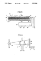
- FIG. 5 shows in schematic representation a cassette like device for using an X-ray panel in accordance with this invention for capturing a latent X-ray image.
- FIG. 6 shows in schematic representation an arrangement for using an X-ray panel in accordance with this invention for capturing a latent X-ray image.
- FIG. 7 represents an electrical equivalent of an element in accordance with the present invention prior to exposure to X-ray radiation.
- FIG. 8 represents an electrical equivalent of an element in accordance with this invention just after exposure to X-ray radiation.
- FIG. 9 represents an electrical equivalent of an element in accordance with this invention just after exposure to X-ray radiation and removal of a bias voltage.
- FIG. 10 represents an electrical equivalent of the element just after a uniform actinic exposure following exposure to X-ray radiation and removal of the bias voltage.
- FIG. 11 is a block diagram of an arrangement for the capture and display of a radiogram in accordance with this invention.
- an X-ray image capture apparatus, element or panel 16 is depicted having a first conductive backing layer 12.
- This conductive backing layer 12 is made of conductive material, and may be rigid or flexible, transparent or non-transparent. Preferably it is a continuous layer made of a sufficiently thick and rigid conductive material to serve as a support for other layers included in the image capture element 16.
- the photoconductive layer 8 preferably exhibits very high dark resistivity.
- the photoconductive layer 8 may comprise amorphous selenium, lead oxide, cadmium sulfide, mercuric iodide or any other such material, including organic materials such as photoconductive polymers preferably loaded with X-ray absorbing compounds, which exhibit photoconductivity.
- exhibiting photoconductivity means that upon exposure to actinic or X-ray radiation, the material exhibits reduced resistivity than in the absence of such exposure.
- the reduced resistivity is in reality the effect of electron hole pairs generated in the material by the incident radiation.
- the change in apparent resistivity is proportional to the intensity of the incident radiation.
- actinic radiation again for purposes of describing the present invention, is meant Ultraviolet (U.V.), infrared (I.R.), visible, or gamma-radiation but excludes X-ray radiation.
- the photoconductive layer 8 should be chosen of sufficient thickness to absorb the incident X-ray radiation, or a substantial portion thereof, to provide high efficiency in radiation detection.
- the specific type of material selected will further depend upon the desired charge retention time, and the desired simplicity of manufacture. Selenium is one preferred such material.
- dielectric layer 6 Over the front surface of photoconductive layer 8 there is applied a dielectric layer 6.
- the dielectric layer 6 must be transparent to both X-ray and actinic radiation and have sufficient thickness to prevent charge leakage. In the preferred embodiment of the present invention, dielectric layer 6 should have a thickness greater than 100 Angstroms.
- Mylar® (i.e., polyethylene terephthalate) sheeting, with a thickness of 50 micrometers may be used for layer 6, although thinner layers are suitable.
- microplates As better shown in FIG. 2, over the dielectric layer 6 there is created a plurality of discrete minute conductive electrodes 4 (i.e., 4a, 4b, 4c, . . . 4n) referred to herein as microplates.
- the dimensions of the microplates define the smallest picture element (PIXEL) resolvable by the element 16.
- the electrodes 4 are substantially transparent to both actinic and X-ray radiation. They are deposited on dielectric layer 6 typically, though not necessarily, using vapor or chemical deposition techniques and can be made of a very thin film of metal, such as gold, silver, aluminum, copper, chromium, titanium, platinum and the like.
- the microplates 4 are made of transparent indium-tin oxide.
- the microplates 4 may be deposited as a continuous layer which is then etched to produce a plurality of individual discrete microplates having dimensions coextensive with a smallest resolvable picture element.
- the microplates 4 may also be produced using laser ablation or photoetching.
- the technology to produce such microplates 4 is well known in the art and is not further discussed herein. A good description of photomicrofabrication techniques is given in "Imaging Processing & Materials," Chapter 18, entitled “Imaging for Microfabrication,” by J. M. Shaw of IBM Watson Research Center.
- Each one of the microplates 4a, 4b, 4c, . . . 4n with the intermediate dielectric photoconductive layer 8, and backing conductive layer 12 form two microcapacitors in series, a first microcapacitor being created between the microplate 4 and the front surface of the photoconductive layer 8 and a second microcapacitor between that same surface and the conductive backing layer 12.
- an optional charge barrier layer 10 (the top surface of which is shown by a dotted line in FIG. 1) is added on top of conductive layer 12.
- the base layer 12 is made of an oxide forming metal such as aluminum.
- the charge barrier layer 10 is provided by an aluminum oxide layer formed on the surface of backing layer 12. In this case, the subsequent coating thereon of a selenium photoconductive layer 8 produces a barrier layer behaving as a blocking diode, inhibiting charge flow in one direction.
- the charge barrier layer 10 may also be a simple insulating layer, such as polyethylene terephthalate, of dimensions comparable to the dielectric layer 6.
- conductive address lines X1, X2, . . . Xn charge lines C1, C2, . . . Cn and sense lines S1, S2, . . . Sn are laid out.
- the Xn and Cn lines are shown parallel to each other while the Sn lines are shown orthogonal to the Xn and Cn lines.
- the Cn lines could also have been laid generally parallel to the Sn lines, or all lines could have been laid out parallel to each other in the spaces between the microplates 4, this being strictly a matter of convenience rather than a necessity.
- the Xn and Sn lines are individually accessible through connectors or leads not specifically illustrated in the drawings, along the sides or edges of the panel 16.
- the Cn lines are all interconnected and accessed through a connector, also on a side or edge of the panel 16.
- a single connector with multiple appropriately assigned contacts for the Xn, Sn and Cn lines may of course be provided.
- the Xn and Cn lines may be constructed from the same indium tin oxide layer used for fabricating the microplates 4, and produced during the aforementioned etching which may be used to make the microplates 4. Then the Sn lines may be created after placing an insulating layer 17 over the Xn and Cn lines. The reverse is of course also possible.
- each microplate 4n Connecting each microplate 4n to a Cn line is a diode 7 comprising P-doped and N-doped materials deposited over the dielectric layer 6 in the space between lines Cn and microplates 4n, as shown in FIGS. 1 and 2. Also in the space between each microplate 4n and conductive lines Xn and Sn, there is built an FET transistor 5 having its gate connected to an Xn line and its source and drain connected to a microplate 4n and an Sn line, respectively.
- the FET transistor 5 may comprise a hydrogenated amorphous silicon (a-Si:H) layer, an insulating layer 15 and conductive electrodes 11, 11' and 11" forming the gate, drain and source, respectively, which are connected to lines Xn, Sn, and the microplate 4n.
- a-Si:H hydrogenated amorphous silicon
- the technology for the creation of the FET transistors 5 and the diodes 7 is well known in the art and not a subject of the present invention. See, for instance, "Modular Series on Solid Devices," Volume 5 of Introduction to Microelectronics Fabrication by R. C. Jaeger, Published by Addison-Wesley in 1988.
- FIG. 3 shows an alternate embodiment of an X-ray capturing element or panel 16' in accordance with the present invention in schematic elevation cross-section.
- the panel 16' again comprises a conductive support or layer 12 having an optional barrier layer 10 thereon.
- a photoconductive layer 8 is coated over the conductive layer 12 or the optional barrier layer 10 as the case may be.
- a plurality of conductive microplates 4a, 4b, 4c, . . . 4n are again created over the insulating layer 6 the same as before.
- a fourth plurality of Y1, Y2, Y3 . . . Yn address lines preferably extending across the Xn lines which are insulated from each other by insulation layer 99.
- Insulation layer 99 material is comparable to that of layer 17.
- two a-Si:H FETs 5' are used connected back to back interconnecting the Xn, Yn, Sn lines and the microplates 4.
- the gates of the two FETs are connected to the Xn and Yn lines, respectively, while the source of one of the FETs 5' is connected to the microplate 4n and the drain of the other one of the FETs 5' is connected to the Sn line.
- the Cn lines are again interconnected and have a single access from outside the panel 16'.
- Each microplate 4 is connected to a Cn line with a diode 7.
- the Xn, Yn, and Sn lines are all individually accessible through appropriate connections preferably along the panel sides or edges.
- the entire element 16 or 16' can be made by depositing successive layers of conductor, insulator, photoconductor, insulator, and conductor upon a substrate.
- the diodes 7 and the FETs 5,5' can then be built in the spaces between the microplates 4 on the dielectric layer 6. Assembly may be accomplished by ion implantation, vapor deposition, vacuum deposition, lamination, sputtering or any other known technique useful to deposit even thickness films.
- the element 16 or 16' may also be fabricated by first building the active transistor and diode layers on a glass substrate. Subsequently, dielectric, selenium and other layers are deposited on top yielding the element 16 or 16'.
- the conductive backing layer 12, the charge barrier layer 10, the photoconductive layer 8 and the dielectric layer 6 are all continuous layers.
- direct deposition of the microplates 4 using masking techniques may be used, the method of manufacturing being one of choice depending on available resources and cost considerations, rather than an essential element of the present invention.
- connecting circuitry for connecting an electrical bias source 30 to the Cn line contact on the panel 16,16' and the backing layer 12, so as to apply a DC bias voltage across element 16,16'.
- switch 32 When switch 32 is closed, the diodes 7 are forward biased and become conducting. The bias voltage then appears across the microplates 4n and the backing layer 12.
- circuitry is also provided for connecting to the panel 16 preferably through a removable connector not illustrated, a plurality of charge detectors 36.
- Each detector 36 is connected to a Sn line.
- the charge detectors 36 may comprise an operational amplifier wired to measure the charge in a capacitive circuit in which the charge from the microcapacitors is directed to, and which produces a voltage output proportional to such charge.
- the output of detectors 36 may be sampled sequentially to obtain an output signal and the technology to do this is well known in the art. It is also possible to use a single charge detector with a sampling network arranged so as to sequentially apply the output of the Sn lines to the detector input FIG. 2a shows such an arrangement. In this case, switches 38 addressed through line 39 sequentially apply the lines Sn to an input of a single charge detector 36.
- the Xn lines are also accessible from outside the panel 16 as stated earlier.
- a switching means not shown in the Figures may be used to address either sequentially or at will each of the Xn lines and to apply a voltage to each Xn line.
- the technology for sequentially addressing a plurality of lines on a panel is well developed and extensively used in the field of flat panel TV displays and need not be elaborated here, as the mode selected to perform such addressing is of no criticality to the subject matter of this invention.
- the Yn lines are also provided with sequential or at will addressing means similar to the means used for the addressing of the Xn lines.
- the plurality of sense lines Sn are all interconnected either on the panel 16' itself, or after exiting the panel 16', and their combined output is directed to the input of a single charge detector 36.
- the panel 16,16' described may include a cassette or enclosure to shield the element from exposure to actinic radiation, much in the manner a cassette shields an X-ray film.
- FIG. 5 shows such an arrangement in which a cassette or enclosure 22 is used.
- the cassette 22 is made of material which is opaque to ambient actinic radiation but transparent to X-rays. Since the ambient levels of gamma radiation are not usually high enough to present any exposure problems, it is not necessary that the material be opaque to gamma radiation. Similarly in the absence of ambient IR radiation, the enclosure need not be opaque thereto.
- the enclosure 22 may include a hinge 24 hingedly connecting a top section 25 and a bottom section 27, allowing the cassette 22 to open and close at will.
- the cassette 22 may further include electrical connecting means 34 which permit one to connect power source 30 via wiring 26 and 28 to the Cn line contact on the panel 16,16'.
- a switching means such as switch 32, is again provided to permit applying and stopping the applying of the bias voltage 30 to the cassette 22. It is also possible to provide the cassette 22 with additional contacts which will permit electrical access to the Xn, Yn and Sn (depending on the panel structure chosen) lines, which may be used to obtain data from the panel 16,16' without removing it from the cassette 22.
- the element 16,16' is placed in cassette 22 and the cassette 22 is placed in the path of information modulated X-ray radiation in a manner similar to the way a traditional cassette-photosensitive film combination is positioned.
- FIG. 6 shows a source of X-ray radiation 44 emitting a beam of X-rays.
- a target 48 i.e., a patient in the case of medical diagnostic imaging, is placed in the X-ray beam path.
- the emerging radiation through the patient 48 is intensity modulated because of the different degree of X-ray absorption in the target 48.
- the modulated X-ray radiation beam 46 is then intercepted by the cassette 22 containing element 16 or 16'.
- X-rays penetrate the enclosure 22 and are eventually absorbed by the photoconductive layer 8 altering its apparent resistivity in proportion to the radiation intensity along the X-ray paths therethrough. Viewed in a different way, the X-rays generate a flow of electron hole pairs, of which the electrons are accumulated in the interface between the photoconductive layer 8 and the dielectric layer 6. Switch 32 is closed during the exposure step in synchronization therewith, or prior thereto, applying a bias D.C. voltage from source 30 to the element 16 or 16'.
- the X-ray flux is interrupted and X-rays no longer impinge on the element 16,16'.
- the application of the bias voltage 30 is then either simultaneously or soon thereafter removed from the element 16,16' by opening the switch 32.
- the cassette 22 may be opened.
- the element 16 can be handled in the presence of actinic radiation without loss of the stored image information contained in it as a charge distribution in the microcapacitors in the dielectric layer 6. The presence of this charge and the operation of the panel 16 in capturing an image in the form of a charge distribution will be explained below.
- the element 16 is intentionally exposed to a large dose of actinic radiation, as by a flash exposure, to eliminate the charges stored in the photoconductive layer 8, by momentarily rendering such photoconductive layer 8 substantially conductive.
- the layer 8 behaves as substantially conductive, because the abundant illumination produces an ample supply of electron hole pairs, in effect, neutralizing any charges stored in the photoconductive layer 8.
- FIG. 7 which represent an equivalent electric circuit of the combination of the transparent electrode 4, the dielectric layer 6, the photoconductive layer 8 and the backing conductive layer 12.
- a variable resistance in dotted lines representing the effect of the electron hole pair generation in the photoconductive layer 8.
- the microcapacitors When voltage supply 30 is connected across the element as shown in FIG. 7, in the absence of actinic or X-ray radiation, the microcapacitors are all charged uniformly the charge being a function of the capacitance of each capacitor. In the present case where all capacitors have the same area plates, the capacitance will depend on the plate separation and dielectric constant of the material between the plates. In the described structure, this will result in two different voltages appearing across the capacitors, one in the capacitors representing the photoconductor layer 8, the other in the dielectric layer 6. If, for instance, the applied voltage difference from the bias source 30 is 2000 Volts, it could be distributed across the two capacitors as 100 volts across the dielectric 6 and 1900 volts across the photoconductor 8.
- FIG. 8 shows schematically such a hypothetical consequential voltage redistribution.
- the switch 32 is opened disconnecting the source 30 from the element 16 and terminating the application of the bias voltage 30 along line 2 to the microplates 4.
- each of the microplates 4 is isolated by the diodes 7 from all others and stands alone.
- FIG. 9 shows the voltage distribution at this point. The charges having nowhere to go remain fixed as they were at the end of the X-ray exposure time period. At this time the voltage source 30 may be completely removed from contact with the element 16 or the cassette 22.
- each capacitor pair The total voltage appearing across each capacitor pair is still 2000 volts. However, the charges in the dielectric portion of each capacitor pair are no longer uniform across the full surface of element 16 (or 16"), but vary representing a latent radiographic image.
- the flash exposure while preferably done using actinic radiation, can also be performed using additional, unmodulated X-ray radiation.
- An electric signal representing the latent radiographic image captured in the microcapacitors of the element 16 as varying amounts of stored electrical charge is read out by exposing the element 16 to uniform actinic radiation and while doing so, sequentially addressing each of the Xn lines and applying a voltage to the gate of the FETs 5 connected to the Xn line. This results in rendering the FETs 5 conductive and sending the charges stored in the corresponding microcapacitors along the Sn lines.
- the charge amplifiers 36 produce each a voltage output proportional to the charge detected on the line Sn.
- the output of the charge detectors 36 may next be sequentially sampled to obtain an electrical signal representing the charge distribution along the addressed Xn line, each microcapacitor representing one image pixel.
- the next Xn line is then addressed and the process repeated till all the microcapacitors have been sampled and the full image has been read out.
- the electrical signal output may be stored or displayed or both.
- the operation is practically identical, differing in that the lines Sn are sampled sequentially rather than the charge detectors outputs, and the sampled Sn line is connected to the one charge detector 36 input to produce an output voltage. This output voltage is then used as before to display or store an image.
- each microplate 4 and corresponding microcapacitor is sampled individually, rather than across a whole line as in FIG. 2a, by using two FETs 5' back to back.
- a voltage appears across a Yn line at the gates of a line of microcapacitors, and another across an Xn line and a corresponding line of microcapacitors.
- the signal obtained from the detector 36 is preferably converted to a digital signal, in an analog to digital (A/D) converter 110, as shown in FIG. 11.
- A/D converter 110 From the A/D converter 110 the signal is directed over line 140 to a computer 142.
- Computer 142 inter alia directs the signal to appropriate storage means which may be both a internal RAM memory or a long term archival memory 144 or both.
- the data representing the radiogram may undergo image processing, such as filtering, contrast enhancement, and the like, and it may be displayed on a CRT 146 for immediate viewing or it may be used in a printer 148 to produce a hard copy 150.
Landscapes
- Physics & Mathematics (AREA)
- Health & Medical Sciences (AREA)
- Life Sciences & Earth Sciences (AREA)
- General Physics & Mathematics (AREA)
- High Energy & Nuclear Physics (AREA)
- Molecular Biology (AREA)
- Spectroscopy & Molecular Physics (AREA)
- Measurement Of Radiation (AREA)
- Conversion Of X-Rays Into Visible Images (AREA)
- Radiography Using Non-Light Waves (AREA)
Abstract
Description
Claims (9)
Priority Applications (4)
| Application Number | Priority Date | Filing Date | Title |
|---|---|---|---|
| US08/044,427 US5313066A (en) | 1992-05-20 | 1993-04-07 | Electronic method and apparatus for acquiring an X-ray image |
| EP93107349A EP0626592B1 (en) | 1992-05-20 | 1993-05-06 | Electronic method and apparatus for acquiring an x-ray image |
| DE69327898T DE69327898T2 (en) | 1992-05-20 | 1993-05-06 | Electronic method and device for acquiring an X-ray image |
| JP11869593A JP2835334B2 (en) | 1992-05-20 | 1993-05-20 | X-ray imaging element and method of forming a radiation image on the element |
Applications Claiming Priority (2)
| Application Number | Priority Date | Filing Date | Title |
|---|---|---|---|
| US88666192A | 1992-05-20 | 1992-05-20 | |
| US08/044,427 US5313066A (en) | 1992-05-20 | 1993-04-07 | Electronic method and apparatus for acquiring an X-ray image |
Related Parent Applications (1)
| Application Number | Title | Priority Date | Filing Date |
|---|---|---|---|
| US88666192A Continuation-In-Part | 1992-05-20 | 1992-05-20 |
Publications (1)
| Publication Number | Publication Date |
|---|---|
| US5313066A true US5313066A (en) | 1994-05-17 |
Family
ID=26721540
Family Applications (1)
| Application Number | Title | Priority Date | Filing Date |
|---|---|---|---|
| US08/044,427 Expired - Fee Related US5313066A (en) | 1992-05-20 | 1993-04-07 | Electronic method and apparatus for acquiring an X-ray image |
Country Status (4)
| Country | Link |
|---|---|
| US (1) | US5313066A (en) |
| EP (1) | EP0626592B1 (en) |
| JP (1) | JP2835334B2 (en) |
| DE (1) | DE69327898T2 (en) |
Cited By (30)
| Publication number | Priority date | Publication date | Assignee | Title |
|---|---|---|---|---|
| US5563421A (en) * | 1995-06-07 | 1996-10-08 | Sterling Diagnostic Imaging, Inc. | Apparatus and method for eliminating residual charges in an image capture panel |
| US5629968A (en) * | 1995-05-12 | 1997-05-13 | Eastman Kodak Company | Apparatus and method for obtaining two radiographic images of an object from one exposing radiation dose |
| US5652430A (en) * | 1996-05-03 | 1997-07-29 | Sterling Diagnostic Imaging, Inc. | Direct radiographic imaging panel |
| US5658186A (en) * | 1996-07-16 | 1997-08-19 | Sterling Diagnostic Imaging, Inc. | Jig for polishing the edge of a thin solid state array panel |
| US5693947A (en) * | 1993-04-28 | 1997-12-02 | The University Of Surrey | Radiation detectors |
| US5827757A (en) * | 1996-07-16 | 1998-10-27 | Direct Radiography Corp. | Fabrication of large area x-ray image capturing element |
| US5852296A (en) * | 1996-06-21 | 1998-12-22 | Kabushiki Kaisha Toshiba | X-ray imaging apparatus |
| US5877501A (en) * | 1996-11-26 | 1999-03-02 | Picker International, Inc. | Digital panel for x-ray image acquisition |
| US5886359A (en) * | 1996-06-13 | 1999-03-23 | Eastman Kodak Company | X-ray dectector, detection assembly, and method |
| US5895936A (en) * | 1997-07-09 | 1999-04-20 | Direct Radiography Co. | Image capture device using a secondary electrode |
| US5956382A (en) * | 1997-09-25 | 1999-09-21 | Eliezer Wiener-Avnear, Doing Business As Laser Electro Optic Application Technology Comp. | X-ray imaging array detector and laser micro-milling method for fabricating array |
| US5994713A (en) * | 1997-06-25 | 1999-11-30 | Quantum Imaging Corp. | Filmless photon imaging apparatus |
| US6025599A (en) * | 1997-12-09 | 2000-02-15 | Direct Radiography Corp. | Image capture element |
| US6181769B1 (en) | 1997-10-01 | 2001-01-30 | Siemens Aktiengesellschaft | X-ray detector with anatomically adapted recess |
| US6243441B1 (en) | 1999-07-13 | 2001-06-05 | Edge Medical Devices | Active matrix detector for X-ray imaging |
| US6281507B1 (en) * | 1999-06-30 | 2001-08-28 | Siemens Medical Systems, Inc. | Interdigital photoconductor structure for direct X-ray detection in a radiography imaging system |
| US6370265B1 (en) | 1999-11-24 | 2002-04-09 | Direct Radiography Corp. | Method for generating gray scale transfer functions for use in displaying a digital radiogram |
| US6381351B1 (en) | 1999-11-24 | 2002-04-30 | Direct Radiography Corp. | Weighted inverse topography method for digital x-ray image data processing |
| US6399950B1 (en) * | 2000-11-27 | 2002-06-04 | Shimadzu Corporation | Two-dimensional radiation detector |
| US20020079458A1 (en) * | 1999-07-26 | 2002-06-27 | Edge Medical Devices Ltd. | Hybrid detector for X-ray imaging |
| US20030010923A1 (en) * | 2001-07-16 | 2003-01-16 | Edge Medical Devices Ltd. | High resolution detector for X-ray imaging |
| US20030169847A1 (en) * | 2001-11-21 | 2003-09-11 | University Of Massachusetts Medical Center | System and method for x-ray fluoroscopic imaging |
| US6791091B2 (en) | 2001-06-19 | 2004-09-14 | Brian Rodricks | Wide dynamic range digital imaging system and method |
| US20040217294A1 (en) * | 1999-07-26 | 2004-11-04 | Albert Zur | Digital detector for X-ray imaging |
| US20040256569A1 (en) * | 2003-06-20 | 2004-12-23 | Shimadzu Corporation | Radiation detector and radiation imaging device equipped with the same |
| US6949749B2 (en) * | 2000-06-08 | 2005-09-27 | Shimadzu Corporation | Electromagnetic imaging apparatus and manufacturing method therefor |
| US20060182326A1 (en) * | 2005-01-20 | 2006-08-17 | Eastman Kodak Company | Radiation therapy method with target detection |
| US20070195937A1 (en) * | 2006-01-16 | 2007-08-23 | Rainer Haupl | Mount for image receiver |
| US20080237481A1 (en) * | 2007-03-29 | 2008-10-02 | Varian Medical Systems Technologies, Inc. | Corrosion barrier layer for photoconductive X-ray imagers |
| US11846739B2 (en) * | 2021-01-12 | 2023-12-19 | Innocare Optoelectronics Corporation | Circuit for sensing X-ray |
Families Citing this family (1)
| Publication number | Priority date | Publication date | Assignee | Title |
|---|---|---|---|---|
| US9660827B2 (en) | 2007-01-12 | 2017-05-23 | Symbol Technologies, Llc | System and method of switching from multicast to unicast calls |
Citations (27)
| Publication number | Priority date | Publication date | Assignee | Title |
|---|---|---|---|---|
| US2866903A (en) * | 1954-11-02 | 1958-12-30 | Berchtold Jean | Process for photoelectric reproductions and apparatus therefor |
| US3748380A (en) * | 1967-09-11 | 1973-07-24 | T Kohashi | Energy-responsive luminescent device |
| US3973146A (en) * | 1974-03-18 | 1976-08-03 | North American Philips Corporation | Signal detector comprising field effect transistors |
| US4030922A (en) * | 1974-09-26 | 1977-06-21 | Fuji Photo Film Co., Ltd. | Image recording method |
| US4085327A (en) * | 1977-01-14 | 1978-04-18 | General Electric Company | Direct charge readout electron radiography apparatus with improved signal-to-noise ratio |
| US4134137A (en) * | 1976-11-01 | 1979-01-09 | Xerox Corporation | Single wire microelectrometer imaging system |
| US4176275A (en) * | 1977-08-22 | 1979-11-27 | Minnesota Mining And Manufacturing Company | Radiation imaging and readout system and method utilizing a multi-layered device having a photoconductive insulative layer |
| US4268750A (en) * | 1979-03-22 | 1981-05-19 | The University Of Texas System | Realtime radiation exposure monitor and control apparatus |
| US4446365A (en) * | 1979-03-22 | 1984-05-01 | University Of Texas System | Electrostatic imaging method |
| EP0125691A2 (en) * | 1983-05-16 | 1984-11-21 | Fuji Photo Film Co., Ltd. | Method for dectecting radiation image |
| US4508966A (en) * | 1982-09-22 | 1985-04-02 | Siemens Aktiengesellschaft | Recording and readout apparatus for X-rays |
| US4535468A (en) * | 1982-09-29 | 1985-08-13 | Siemens Aktiengesellschaft | Image converted for X-ray equipment and the like |
| US4539591A (en) * | 1979-03-22 | 1985-09-03 | University Of Texas System | Method of impressing and reading out a surface charge on a multi-layered detector structure |
| US4554453A (en) * | 1983-04-05 | 1985-11-19 | Siemens Aktiengesellschaft | Apparatus for recording X-ray images |
| US4663526A (en) * | 1984-12-26 | 1987-05-05 | Emil Kamieniecki | Nondestructive readout of a latent electrostatic image formed on an insulating material |
| US4670765A (en) * | 1984-04-02 | 1987-06-02 | Sharp Kabushiki Kaisha | Semiconductor photodetector element |
| US4694317A (en) * | 1984-10-22 | 1987-09-15 | Fuji Photo Film Co., Ltd. | Solid state imaging device and process for fabricating the same |
| JPS633454A (en) * | 1986-06-24 | 1988-01-08 | Seiko Epson Corp | Solid-state image sensing device and manufacture thereof |
| US4818857A (en) * | 1986-10-10 | 1989-04-04 | Thomson-Csf | Electrostatic image sensor having an electret which polarizes a photoconductive layer |
| US4857723A (en) * | 1987-09-14 | 1989-08-15 | Texas Medical Instruments, Inc. | Segmented imaging plate structure |
| US4961209A (en) * | 1987-12-01 | 1990-10-02 | Noranda, Inc. | System for measuring the charge distribution on a photoreceptor surface |
| US4975935A (en) * | 1988-12-17 | 1990-12-04 | U.S. Philips Corporation | Method of producing an X-ray exposure by means of a photoconductor and arrangement for carrying out the method |
| US5059794A (en) * | 1987-04-17 | 1991-10-22 | Hitachi, Ltd. | Radiation imaging sensor |
| US5127038A (en) * | 1991-06-28 | 1992-06-30 | E. I. Du Pont De Nemours And Company | Method for capturing and displaying a latent radiographic image |
| US5166524A (en) * | 1991-06-28 | 1992-11-24 | E. I. Du Pont De Nemours & Company | Element, device and associated method for capturing a latent radiographic image |
| US5168160A (en) * | 1991-06-28 | 1992-12-01 | E. I. Du Pont De Nemours And Company | Method and apparatus for acquiring an electrical signal representing a radiographic image |
| US5182624A (en) * | 1990-08-08 | 1993-01-26 | Minnesota Mining And Manufacturing Company | Solid state electromagnetic radiation detector fet array |
Family Cites Families (2)
| Publication number | Priority date | Publication date | Assignee | Title |
|---|---|---|---|---|
| US4778985A (en) * | 1987-09-14 | 1988-10-18 | Texas Medical Instruments, Inc. | Imaging plate structure |
| US4996413A (en) * | 1990-02-27 | 1991-02-26 | General Electric Company | Apparatus and method for reading data from an image detector |
-
1993
- 1993-04-07 US US08/044,427 patent/US5313066A/en not_active Expired - Fee Related
- 1993-05-06 EP EP93107349A patent/EP0626592B1/en not_active Expired - Lifetime
- 1993-05-06 DE DE69327898T patent/DE69327898T2/en not_active Expired - Fee Related
- 1993-05-20 JP JP11869593A patent/JP2835334B2/en not_active Expired - Fee Related
Patent Citations (29)
| Publication number | Priority date | Publication date | Assignee | Title |
|---|---|---|---|---|
| US2866903A (en) * | 1954-11-02 | 1958-12-30 | Berchtold Jean | Process for photoelectric reproductions and apparatus therefor |
| US3748380A (en) * | 1967-09-11 | 1973-07-24 | T Kohashi | Energy-responsive luminescent device |
| US3973146A (en) * | 1974-03-18 | 1976-08-03 | North American Philips Corporation | Signal detector comprising field effect transistors |
| US4030922A (en) * | 1974-09-26 | 1977-06-21 | Fuji Photo Film Co., Ltd. | Image recording method |
| US4134137A (en) * | 1976-11-01 | 1979-01-09 | Xerox Corporation | Single wire microelectrometer imaging system |
| US4085327A (en) * | 1977-01-14 | 1978-04-18 | General Electric Company | Direct charge readout electron radiography apparatus with improved signal-to-noise ratio |
| US4176275A (en) * | 1977-08-22 | 1979-11-27 | Minnesota Mining And Manufacturing Company | Radiation imaging and readout system and method utilizing a multi-layered device having a photoconductive insulative layer |
| US4268750A (en) * | 1979-03-22 | 1981-05-19 | The University Of Texas System | Realtime radiation exposure monitor and control apparatus |
| US4446365A (en) * | 1979-03-22 | 1984-05-01 | University Of Texas System | Electrostatic imaging method |
| US4539591A (en) * | 1979-03-22 | 1985-09-03 | University Of Texas System | Method of impressing and reading out a surface charge on a multi-layered detector structure |
| US4521808A (en) * | 1979-03-22 | 1985-06-04 | University Of Texas System | Electrostatic imaging apparatus |
| US4508966A (en) * | 1982-09-22 | 1985-04-02 | Siemens Aktiengesellschaft | Recording and readout apparatus for X-rays |
| US4535468A (en) * | 1982-09-29 | 1985-08-13 | Siemens Aktiengesellschaft | Image converted for X-ray equipment and the like |
| US4554453A (en) * | 1983-04-05 | 1985-11-19 | Siemens Aktiengesellschaft | Apparatus for recording X-ray images |
| EP0125691A2 (en) * | 1983-05-16 | 1984-11-21 | Fuji Photo Film Co., Ltd. | Method for dectecting radiation image |
| US4670765A (en) * | 1984-04-02 | 1987-06-02 | Sharp Kabushiki Kaisha | Semiconductor photodetector element |
| US4694317A (en) * | 1984-10-22 | 1987-09-15 | Fuji Photo Film Co., Ltd. | Solid state imaging device and process for fabricating the same |
| US4663526A (en) * | 1984-12-26 | 1987-05-05 | Emil Kamieniecki | Nondestructive readout of a latent electrostatic image formed on an insulating material |
| US4873436A (en) * | 1985-04-03 | 1989-10-10 | Optical Diagnostic Systems, Inc. | Nondestructive readout of a latent electrostatic image formed on an insulating material |
| JPS633454A (en) * | 1986-06-24 | 1988-01-08 | Seiko Epson Corp | Solid-state image sensing device and manufacture thereof |
| US4818857A (en) * | 1986-10-10 | 1989-04-04 | Thomson-Csf | Electrostatic image sensor having an electret which polarizes a photoconductive layer |
| US5059794A (en) * | 1987-04-17 | 1991-10-22 | Hitachi, Ltd. | Radiation imaging sensor |
| US4857723A (en) * | 1987-09-14 | 1989-08-15 | Texas Medical Instruments, Inc. | Segmented imaging plate structure |
| US4961209A (en) * | 1987-12-01 | 1990-10-02 | Noranda, Inc. | System for measuring the charge distribution on a photoreceptor surface |
| US4975935A (en) * | 1988-12-17 | 1990-12-04 | U.S. Philips Corporation | Method of producing an X-ray exposure by means of a photoconductor and arrangement for carrying out the method |
| US5182624A (en) * | 1990-08-08 | 1993-01-26 | Minnesota Mining And Manufacturing Company | Solid state electromagnetic radiation detector fet array |
| US5127038A (en) * | 1991-06-28 | 1992-06-30 | E. I. Du Pont De Nemours And Company | Method for capturing and displaying a latent radiographic image |
| US5166524A (en) * | 1991-06-28 | 1992-11-24 | E. I. Du Pont De Nemours & Company | Element, device and associated method for capturing a latent radiographic image |
| US5168160A (en) * | 1991-06-28 | 1992-12-01 | E. I. Du Pont De Nemours And Company | Method and apparatus for acquiring an electrical signal representing a radiographic image |
Non-Patent Citations (11)
| Title |
|---|
| E. B. Lipscomb, III, Structural Limitations in Method Claims, Walker on Patents, 3, 11 12, 1985. * |
| E. B. Lipscomb, III, Structural Limitations in Method Claims, Walker on Patents, 3, 11-12, 1985. |
| L. E. Antonuk et al., Development of Hydrogenated Amorphous Silicon Sensors for Diagnostic X Rays Imaging, IEEE Transactions on Nuclear Science, 38, No. 2, Apr. 1991. * |
| L. E. Antonuk et al., Development of Hydrogenated Amorphous Silicon Sensors for Diagnostic X-Rays Imaging, IEEE Transactions on Nuclear Science, 38, No. 2, Apr. 1991. |
| L. E. Antonuk et al., Development of Hydrogenated Amorphous Silicon Sensors for High Energy Photon Radiotherapy Imaging, IEEE Transactions on Nuclear Science, 37, No. 2, Apr. 1990. * |
| L. E. Antonuk et al., Development of Thin Film, Flat Panel Arrays for Diagnostic and Radiotherapy Imaging, Conference Proceedings of SPIE Medical Imaging VI, Newport Beach, Calif., Feb. 23 27, 1992. * |
| L. E. Antonuk et al., Development of Thin Film, Flat Panel Arrays for Diagnostic and Radiotherapy Imaging, Conference Proceedings of SPIE Medical Imaging VI, Newport Beach, Calif., Feb. 23-27, 1992. |
| L. E. Antonuk et al., Large Area Amorphous Silicon Photodiode Arrays for Radiotherapy and Diagnostic Imaging, Nuclear Instruments and Methods in Physics Research, A310, 460 464, 1991. * |
| L. E. Antonuk et al., Large Area Amorphous Silicon Photodiode Arrays for Radiotherapy and Diagnostic Imaging, Nuclear Instruments and Methods in Physics Research, A310, 460-464, 1991. |
| L. E. Antonuk et al., Signal, Noise, and Readout Considerations in the Development of Amorphous Silicon Photodiode Arrays for Radiotherapy and Diagnostic X Ray Imaging, Medical Imaging V: Imaging Physics, 1443, 108 119, Feb. 25 26, 1991. * |
| L. E. Antonuk et al., Signal, Noise, and Readout Considerations in the Development of Amorphous Silicon Photodiode Arrays for Radiotherapy and Diagnostic X-Ray Imaging, Medical Imaging V: Imaging Physics, 1443, 108-119, Feb. 25-26, 1991. |
Cited By (39)
| Publication number | Priority date | Publication date | Assignee | Title |
|---|---|---|---|---|
| US5693947A (en) * | 1993-04-28 | 1997-12-02 | The University Of Surrey | Radiation detectors |
| US5629968A (en) * | 1995-05-12 | 1997-05-13 | Eastman Kodak Company | Apparatus and method for obtaining two radiographic images of an object from one exposing radiation dose |
| US5563421A (en) * | 1995-06-07 | 1996-10-08 | Sterling Diagnostic Imaging, Inc. | Apparatus and method for eliminating residual charges in an image capture panel |
| US5652430A (en) * | 1996-05-03 | 1997-07-29 | Sterling Diagnostic Imaging, Inc. | Direct radiographic imaging panel |
| US5886359A (en) * | 1996-06-13 | 1999-03-23 | Eastman Kodak Company | X-ray dectector, detection assembly, and method |
| US5852296A (en) * | 1996-06-21 | 1998-12-22 | Kabushiki Kaisha Toshiba | X-ray imaging apparatus |
| US5658186A (en) * | 1996-07-16 | 1997-08-19 | Sterling Diagnostic Imaging, Inc. | Jig for polishing the edge of a thin solid state array panel |
| US5827757A (en) * | 1996-07-16 | 1998-10-27 | Direct Radiography Corp. | Fabrication of large area x-ray image capturing element |
| US5877501A (en) * | 1996-11-26 | 1999-03-02 | Picker International, Inc. | Digital panel for x-ray image acquisition |
| US5994713A (en) * | 1997-06-25 | 1999-11-30 | Quantum Imaging Corp. | Filmless photon imaging apparatus |
| US5895936A (en) * | 1997-07-09 | 1999-04-20 | Direct Radiography Co. | Image capture device using a secondary electrode |
| US5956382A (en) * | 1997-09-25 | 1999-09-21 | Eliezer Wiener-Avnear, Doing Business As Laser Electro Optic Application Technology Comp. | X-ray imaging array detector and laser micro-milling method for fabricating array |
| US6181769B1 (en) | 1997-10-01 | 2001-01-30 | Siemens Aktiengesellschaft | X-ray detector with anatomically adapted recess |
| US6025599A (en) * | 1997-12-09 | 2000-02-15 | Direct Radiography Corp. | Image capture element |
| US6281507B1 (en) * | 1999-06-30 | 2001-08-28 | Siemens Medical Systems, Inc. | Interdigital photoconductor structure for direct X-ray detection in a radiography imaging system |
| US6243441B1 (en) | 1999-07-13 | 2001-06-05 | Edge Medical Devices | Active matrix detector for X-ray imaging |
| US20040217294A1 (en) * | 1999-07-26 | 2004-11-04 | Albert Zur | Digital detector for X-ray imaging |
| US20020079458A1 (en) * | 1999-07-26 | 2002-06-27 | Edge Medical Devices Ltd. | Hybrid detector for X-ray imaging |
| US6900442B2 (en) * | 1999-07-26 | 2005-05-31 | Edge Medical Devices Ltd. | Hybrid detector for X-ray imaging |
| US6864484B1 (en) * | 1999-07-26 | 2005-03-08 | Edge Medical Devices, Ltd | Digital detector for x-ray imaging |
| US6370265B1 (en) | 1999-11-24 | 2002-04-09 | Direct Radiography Corp. | Method for generating gray scale transfer functions for use in displaying a digital radiogram |
| US6381351B1 (en) | 1999-11-24 | 2002-04-30 | Direct Radiography Corp. | Weighted inverse topography method for digital x-ray image data processing |
| US6949749B2 (en) * | 2000-06-08 | 2005-09-27 | Shimadzu Corporation | Electromagnetic imaging apparatus and manufacturing method therefor |
| US6399950B1 (en) * | 2000-11-27 | 2002-06-04 | Shimadzu Corporation | Two-dimensional radiation detector |
| US6791091B2 (en) | 2001-06-19 | 2004-09-14 | Brian Rodricks | Wide dynamic range digital imaging system and method |
| US6784433B2 (en) | 2001-07-16 | 2004-08-31 | Edge Medical Devices Ltd. | High resolution detector for X-ray imaging |
| US20030010923A1 (en) * | 2001-07-16 | 2003-01-16 | Edge Medical Devices Ltd. | High resolution detector for X-ray imaging |
| US6895077B2 (en) | 2001-11-21 | 2005-05-17 | University Of Massachusetts Medical Center | System and method for x-ray fluoroscopic imaging |
| US20030169847A1 (en) * | 2001-11-21 | 2003-09-11 | University Of Massachusetts Medical Center | System and method for x-ray fluoroscopic imaging |
| US7420178B2 (en) * | 2003-06-20 | 2008-09-02 | Shimadzu Corporation | Radiation detector and radiation imaging device equipped with the same |
| US20040256569A1 (en) * | 2003-06-20 | 2004-12-23 | Shimadzu Corporation | Radiation detector and radiation imaging device equipped with the same |
| US20060182326A1 (en) * | 2005-01-20 | 2006-08-17 | Eastman Kodak Company | Radiation therapy method with target detection |
| US7453983B2 (en) | 2005-01-20 | 2008-11-18 | Carestream Health, Inc. | Radiation therapy method with target detection |
| US20070195937A1 (en) * | 2006-01-16 | 2007-08-23 | Rainer Haupl | Mount for image receiver |
| US7497616B2 (en) * | 2006-01-16 | 2009-03-03 | Siemens Aktiengesellschaft | Mount for image receiver |
| DE102006002083B4 (en) * | 2006-01-16 | 2009-06-10 | Siemens Ag | Holder with x-ray detector |
| US20080237481A1 (en) * | 2007-03-29 | 2008-10-02 | Varian Medical Systems Technologies, Inc. | Corrosion barrier layer for photoconductive X-ray imagers |
| US8232531B2 (en) | 2007-03-29 | 2012-07-31 | Varian Medical Systems, Inc. | Corrosion barrier layer for photoconductive X-ray imagers |
| US11846739B2 (en) * | 2021-01-12 | 2023-12-19 | Innocare Optoelectronics Corporation | Circuit for sensing X-ray |
Also Published As
| Publication number | Publication date |
|---|---|
| DE69327898D1 (en) | 2000-03-30 |
| JPH06130196A (en) | 1994-05-13 |
| EP0626592B1 (en) | 2000-02-23 |
| JP2835334B2 (en) | 1998-12-14 |
| DE69327898T2 (en) | 2000-10-05 |
| EP0626592A3 (en) | 1997-04-02 |
| EP0626592A2 (en) | 1994-11-30 |
Similar Documents
| Publication | Publication Date | Title |
|---|---|---|
| US5313066A (en) | Electronic method and apparatus for acquiring an X-ray image | |
| US5331179A (en) | Method and apparatus for acquiring an X-ray image using a thin film transistor array | |
| EP0602475B1 (en) | Method and apparatus for acquiring an X-ray image using a solid state device | |
| EP0603709B1 (en) | Electronic cassette for recording X-ray images | |
| US5168160A (en) | Method and apparatus for acquiring an electrical signal representing a radiographic image | |
| US5498880A (en) | Image capture panel using a solid state device | |
| US5166524A (en) | Element, device and associated method for capturing a latent radiographic image | |
| EP0437041B1 (en) | Solid-state radiation sensors | |
| JP3457676B2 (en) | Radiation imaging panel | |
| US5127038A (en) | Method for capturing and displaying a latent radiographic image | |
| US5969360A (en) | Readout sequence for residual image elimination in a radiation detection panel | |
| US5895936A (en) | Image capture device using a secondary electrode | |
| US6025599A (en) | Image capture element | |
| EP0574689B1 (en) | Method and appparatus for acquiring an X-ray image using a thin film transistor array | |
| US6194727B1 (en) | Direct radiographic imaging panel having a dielectric layer with an adjusted time constant | |
| WO1994004963A1 (en) | Element, device and associated method for capturing a latent radiographic image | |
| EP1018655B1 (en) | Readout sequence for residual image elimination in a radiation detection panel | |
| Den Boer et al. | Thin-film transistor array technology for high-performance direct-conversion x-ray sensors | |
| EP1018768A1 (en) | Image capture element | |
| EP1342105A2 (en) | Direct radiographic imaging panel with an imaging property reversibly adjustable with an external energy source in clinical use of the panel |
Legal Events
| Date | Code | Title | Description |
|---|---|---|---|
| AS | Assignment |
Owner name: E.I. DU PONT DE NEMOURS AND COMPANY, DELAWARE Free format text: ASSIGNMENT OF ASSIGNORS INTEREST;ASSIGNORS:LEE, DENNY LAP YEN;JEROMIN, LOTHAR SIEGFRIED;REEL/FRAME:006487/0846 Effective date: 19930407 |
|
| AS | Assignment |
Owner name: TEXAS COMMERCE BANK NATIONAL ASSOCIATION, TEXAS Free format text: SECURITY INTEREST;ASSIGNOR:STERLING DIAGNOSTIC IMAGING, INC.;REEL/FRAME:007919/0405 Effective date: 19960329 |
|
| AS | Assignment |
Owner name: STERLING DIAGNOSTIC IMAGING, INC., DELAWARE Free format text: ASSIGNMENT OF ASSIGNORS INTEREST;ASSIGNOR:E. I. DU PONT DE NEMOURS AND COMPANY;REEL/FRAME:008246/0967 Effective date: 19960329 |
|
| AS | Assignment |
Owner name: TEXAS COMMERCE BANK NATIONAL ASSOCIATION, AS ADMIN Free format text: SECURITY AGREEMENT;ASSIGNOR:STERLING DIAGNOSTIC IMAGING, INC.;REEL/FRAME:008698/0513 Effective date: 19970825 |
|
| FPAY | Fee payment |
Year of fee payment: 4 |
|
| AS | Assignment |
Owner name: DIRECT RADIOGRAPHY CORP., DELAWARE Free format text: ASSIGNMENT OF ASSIGNORS INTEREST;ASSIGNOR:DRC HOLDING CORP.;REEL/FRAME:010461/0316 Effective date: 19990513 |
|
| FPAY | Fee payment |
Year of fee payment: 8 |
|
| REMI | Maintenance fee reminder mailed | ||
| LAPS | Lapse for failure to pay maintenance fees | ||
| STCH | Information on status: patent discontinuation |
Free format text: PATENT EXPIRED DUE TO NONPAYMENT OF MAINTENANCE FEES UNDER 37 CFR 1.362 |
|
| FP | Lapsed due to failure to pay maintenance fee |
Effective date: 20060517 |