US5253096A - Digital pulse optical transmitter and receiver for local area network applications - Google Patents

Digital pulse optical transmitter and receiver for local area network applications Download PDF

Info

Publication number
US5253096A
US5253096A US07/788,848 US78884891A US5253096A US 5253096 A US5253096 A US 5253096A US 78884891 A US78884891 A US 78884891A US 5253096 A US5253096 A US 5253096A
Authority
US
United States
Prior art keywords
pulse
optical transmitter
optical
sub
receiver
Prior art date
Legal status (The legal status is an assumption and is not a legal conclusion. Google has not performed a legal analysis and makes no representation as to the accuracy of the status listed.)
Expired - Fee Related
Application number
US07/788,848
Inventor
William R. Freeman
Bhavesh Patel
Current Assignee (The listed assignees may be inaccurate. Google has not performed a legal analysis and makes no representation or warranty as to the accuracy of the list.)
Raylan Corp
Original Assignee
Raylan Corp
Priority date (The priority date is an assumption and is not a legal conclusion. Google has not performed a legal analysis and makes no representation as to the accuracy of the date listed.)
Filing date
Publication date
Application filed by Raylan Corp filed Critical Raylan Corp
Priority to US07/788,848 priority Critical patent/US5253096A/en
Assigned to RAYLAN CORPORATION reassignment RAYLAN CORPORATION ASSIGNMENT OF ASSIGNORS INTEREST. Assignors: FREEMAN, WILLIAM R., PATEL, BHAVESH
Application granted granted Critical
Publication of US5253096A publication Critical patent/US5253096A/en
Anticipated expiration legal-status Critical
Expired - Fee Related legal-status Critical Current

Links

Images

Classifications

    • HELECTRICITY
    • H04ELECTRIC COMMUNICATION TECHNIQUE
    • H04BTRANSMISSION
    • H04B10/00Transmission systems employing electromagnetic waves other than radio-waves, e.g. infrared, visible or ultraviolet light, or employing corpuscular radiation, e.g. quantum communication
    • H04B10/50Transmitters
    • H04B10/501Structural aspects
    • H04B10/503Laser transmitters
    • H04B10/504Laser transmitters using direct modulation
    • HELECTRICITY
    • H04ELECTRIC COMMUNICATION TECHNIQUE
    • H04BTRANSMISSION
    • H04B10/00Transmission systems employing electromagnetic waves other than radio-waves, e.g. infrared, visible or ultraviolet light, or employing corpuscular radiation, e.g. quantum communication
    • H04B10/50Transmitters
    • H04B10/508Pulse generation, e.g. generation of solitons
    • HELECTRICITY
    • H04ELECTRIC COMMUNICATION TECHNIQUE
    • H04BTRANSMISSION
    • H04B10/00Transmission systems employing electromagnetic waves other than radio-waves, e.g. infrared, visible or ultraviolet light, or employing corpuscular radiation, e.g. quantum communication
    • H04B10/50Transmitters
    • H04B10/58Compensation for non-linear transmitter output
    • HELECTRICITY
    • H04ELECTRIC COMMUNICATION TECHNIQUE
    • H04BTRANSMISSION
    • H04B10/00Transmission systems employing electromagnetic waves other than radio-waves, e.g. infrared, visible or ultraviolet light, or employing corpuscular radiation, e.g. quantum communication
    • H04B10/60Receivers
    • H04B10/66Non-coherent receivers, e.g. using direct detection
    • H04B10/67Optical arrangements in the receiver
    • H04B10/671Optical arrangements in the receiver for controlling the input optical signal
    • H04B10/672Optical arrangements in the receiver for controlling the input optical signal for controlling the power of the input optical signal
    • H04B10/673Optical arrangements in the receiver for controlling the input optical signal for controlling the power of the input optical signal using an optical preamplifier

Definitions

  • the present invention relates to optical transmitters and receivers for use in fiber optic local area networks.
  • FIG. 1a shows, however, the functional block diagram of a transmitter system according to the prior art for transmitting an optical information signal.
  • an electrical information signal is processed by pre-processing circuitry 11 before being provided to a drive circuit 13.
  • the drive circuit 13 drives a laser light source 17 that produces an optical output signal.
  • it is normal to monitor both the temperature and the output light intensity of the laser light source 17.
  • the monitoring is accomplished in the illustrated system by temperature monitoring circuitry 21 and optical monitoring circuitry 15, respectively.
  • the temperature monitoring circuitry 21 is used to control a cooling mechanism 19 that prevents overheating of the laser light source 17.
  • the optical monitoring circuitry 15 produces a control input to the drive circuit 13 to control the energy with which the laser light source 17 is driven.
  • the light signal produced by the laser light source 17 normally is transmitted through a light guide or optical fiber, at the receiving end of which the light signal is received by a receiver system such as the digital optical receiver shown in FIG. 1b.
  • incoming light is detected by a detector 23 to produce a low-level electrical signal.
  • the detector output is amplified by a low-noise pre-amplifier 25. Further amplification is performed in a post-amplifier 27, the output of which is shaped by a shaping filter 29 to produce a final signal.
  • the transmitted digital information is extracted from the final signal by a timing circuit 33 and a decision circuit 31 to replicate the original information signal. It may be noted that FIG. 1b does not show a LO-LITE circuit for determining if the received light signal is too weak to be properly received.
  • a particular problem encountered in optical transmitters of the prior art has been pulse width distortion by the inequality of a non-negligible turn-on delay of the typical optical light source and an essentially negligible turn-off delay.
  • the turn-on delay may be, for example, three nanoseconds and the turn-off delay may be a small fraction of a nanosecond. If the optical light source is driven by a pulse train comprised of pulses 50 ns wide, then the first 3 ns of each pulse will be spent turning on the optical light source such that the leading edge of each pulse of the resulting optical pulse train is delayed by 3 ns. This problem is illustrated in FIG.
  • the circuit instead of two pulses of 50 ns separated by an interval of 100 ns, the circuit produces an optical pulse train of two 47 ns pulses separated by an interval of 103 ns.
  • the pulse width distortion is 6%, an unacceptable figure in many applications.
  • the present invention provides an optical transmitter and receiver for use in a fiber optic LAN which is characterized by reduced pulse-width distortion, low noise, simplicity of design, and advantageous use of widely-available low-cost components.
  • pulse-width distortion of an optical transmitter is reduced using a pulse input and conditioning means that quickly passes a portion of the injected pulse energy injected to minimize the turn-on delay of an associated optical source, at the same time storing a portion of the pulse energy for release when the injected pulse energy subsides so as to maintain the optical source in an ON state for a time closely approximating the source's turn-on delay.
  • a pre-amplifier portion of an optical receiver is of the trans-impedance type, having a low-noise first stage and a moderate-gain second stage connected to the first stage by feedback means including a resistance on the order of a few kilo-ohms.
  • the low impedance of the feedback means minimizes thermal noise, whereas the moderate gain of the second stage still allows a high trans-impedance to be achieved.
  • a wide bandwidth LO-LITE circuit consists essentially of a DC-blocking capacitor, a single transistor with associated biasing network, an RC compensation network to compensate for frequency-gain characteristics of an amplifier preceding the LO-LITE circuit, an integrator, and a comparator.
  • the present invention provides an optical transmitter having reduced pulse width distortion.
  • the present invention also provides an optical receiver with a low-noise pre-amplifier.
  • FIG. 1a is a functional block diagram of an optical transmitter according to the prior art
  • FIG. 1b is a functional block diagram of an optical receiver according to the prior art
  • FIG. 2a is a schematic diagram of an optical transmitter according to the present invention.
  • FIG. 2b is a schematic diagram of an optical receiver according to the present invention.
  • FIG. 2c is a schematic diagram of a power supply network for the optical receiver of FIG. 2b according to the present invention.
  • FIG. 3 is an enlarged view of the optical transmitter of FIG. 2a;
  • FIG. 4 is an enlarged view of the pre-amplifier portion of the optical receiver of FIG. 2b;
  • FIG. 5 is an enlarged view of part of a LO-LITE circuit portion of FIG. 2b;
  • FIG. 6 is a diagrammatic illustration of the problem of pulse-width distortion in the prior art
  • FIG. 7a is an approximate plot of the frequency-gain characteristic of a main amplifier portion of the optical receiver of FIG. 2b.
  • FIG. 7b is an approximate plot of the frequency-gain characteristic of the LO-LITE circuit portion of the optical receiver of FIG. 2b.
  • R, L, C, and so forth are used to designate resistors, inductors, capacitors and other electronic components in conventional fashion are followed by a subscript notation indicating in which of FIGS. 3-5 that component appears. For simplicity, this convention is not observed in FIGS. 3-5 themselves.
  • the first portion of an optical receiver circuitry comprises a low-noise pre-amplifier 41 and a second portion of the optical receiver circuitry comprises a main amplifier 43.
  • the main amplifier 43 provides complementary outputs, respectively, to a signal-shaping filter 44 to produce a final electrical signal E -- OUT and to a LO-LITE circuit to produce a LO-LITE output.
  • the pre-amplifier 41 and the LO-LITE circuit 45 will be described in greater detail in connection with FIGS. 4 and 5 hereafter.
  • a laser semiconductor diode is optically coupled to the end of an optical fiber and is electrically coupled by a three terminal connection 49 to the optical transmitter circuitry.
  • the laser is driven through a current-limiting resistor R4.sub.(3) by a transistor T1.sub.(3) supplied with power through a resistor R2.sub.(3).
  • Power is also supplied through a resistor R3.sub.(3) to reverse bias a back facet monitor (commonly a photodiode) of the semiconductor laser which may be used to perform the optical monitoring function of block 15 of FIG. 1a. In the present embodiment, however, the monitoring output otherwise available at the laser side of resistor R3.sub.(3) is not used.
  • Capacitors C1 and C2 minimize ripple in the power supply voltage.
  • the optical transmitter of FIG. 3 includes a pulse conditioning network for driving the transistor T1.sub.(3).
  • the optical transmitter includes an inductor L1.sub.(3), a resistor R1.sub.(3) and a diode D1.sub.(3).
  • an information pulse signal is first supplied to the pulse conditioning network, a rush of current flows through the diode D1.sub.(3) to quickly turn on the transistor T1.sub.(3) and activate the laser diode.
  • a portion of the energy of the pulse determined by resistors R1.sub.(3) and R5.sub.(3) is stored in the inductor L1.sub.(3).
  • the detector and pre-amplifier portions of the optical receiver of the present invention function to detect a series of light pulses as produced, for example, by the optical transmitter of FIG. 3, convert those pulses into a low-level electrical signal and amplify the low-level electrical signal into an intermediate level electrical signal in as noise-free a manner as possible.
  • a PIN photo diode is used as the detector element, and is optically coupled to an optical fiber and electrically coupled to a three-terminal connector 51.
  • the PIN photo diode is reversed biased by a resistor R1.sub.(4) connected to power.
  • the detection output of the PIN photo diode is input to one of the gates of a dual-gate MOSFET T1.sub.(4) used to realize the first stage of the pre-amplifier.
  • a MOSFET is chosen because of its characteristically low noise.
  • a dual-gate MOSFET in particular is chosen so that the amplification of the first stage may be controlled using the second gate.
  • the second gate is set to a potential of about 4 V by means of the resistive divider network R2.sub.(4) and R5.sub.(4) and the stabilizing capacitor C1.sub.(4).
  • the dual-gate MOSFET is biased by resistors R3.sub.(4) and R6.sub.(4). The latter resistor is connected in shunt with a capacitor C2.sub.(4) whose value may be adjusted to adjust the frequency response of the pre-amplifier.
  • the output of the first dual-gate MOSFET stage is input to a second stage realized by a conventional bipolar NPN transistor T2.sub.(4) biased via resistors R4.sub.(4) and R7.sub.(4) so as to achieve an amplification of about 6 or 7.
  • a feedback path is provided from the emitter of the transistor T2.sub.(4) to the input of the MOSFET via feedback resistor R f .
  • thermal noise in an electrical component increases linearly as the impedance of that component, as is well-known in the art. Thermal noise is the chief limiting factor of the sensitivity of the optical receiver.
  • the thermal noise of the pre-amplifier is reduced by using a relatively small feedback resistor R f (for example of approximately 1.5 kilo-ohms), at the same time biasing the second stage transistor T2.sub.(4) so as to achieve a moderate gain of about 6 or 7.
  • R f for example of approximately 1.5 kilo-ohms
  • the output of the second stage is input to a final buffer stage realized using an NPN transistor T3.sub.(4) and associated resistor R8.sub.(4).
  • the output of pre-amplifier portion of the optical receiver is taken at the emitter of the transistor T3.sub.(4).
  • Optical LANs are typically provided with a LO-LITE circuit that compares the level of a received light signal to a specified threshold to determine when the light signal is too weak to be properly received.
  • a LO-LITE condition is detected, the output of the optical receiver (E -- OUT in FIG. 2b) is suspended.
  • the LO-LITE circuit of the present invention presents a very simple single-transistor circuit for LAN applications but is designed to cover a broad frequency range of 100 KHz to 16 MHz in cooperation with the pre-amplifier and the main amplifier of the optical receiver.
  • the single transistor is a conventional NPN bipolar transistor T1.sub.(5) biased via resistors R5.sub.(5), R6.sub.(5) and R3.sub.(5).
  • a DC blocking capacitor C B forms the input of the LO-LITE circuit and is connected to the base of the transistor T1.sub.(5).
  • a diode D1.sub.(5) Connected to the collector of the transistor T1.sub.(5) is a diode D1.sub.(5) through which an integrator composed of the shunt combination of a capacitor C4.sub.(5) and a resistor R4.sub.(5) is charged. The output of the integrator is compared with an appropriate threshold to determine when a LO-LITE condition exists.
  • a stabilizing capacitor C3.sub.(5) stabilizes power supply to the LO-LITE circuit.
  • the main amplifier of the optical receiver exhibits a frequency-gain characteristic that trails off in the vicinity of 16 MHz.
  • the LO-LITE circuit of the present invention is designed to exhibit a frequency-gain characteristic as illustrated in FIG. 7b such that the characteristic exhibits a peak B in the vicinity of 16 MHz where the characteristic of the main amplifier trails off.
  • the lower cutoff frequency of the LO-LITE circuit occurs at a knee A portion of the characteristic in the vicinity of about 100 KHz.
  • two RC pairs, R1C1.sub.(5) and R2C2.sub.(5) realize two zeros, one at approximately 100 KHz to yield the knee A of the frequency-gain response of FIG. 7a and another at approximately 16 MHz to yield the peak B to compensate for gain error caused by the main amplifier.
  • a very simple single-transistor LO-LITE circuit is enabled to operate over a relatively wide frequency range.
  • the features of the present invention described above allow a fiber optic LAN having a favorable cost-performance ratio to be achieved.
  • the LO-LITE of the circuit of the present invention provides a very simple and economical circuit that operates over a wide bandwidth.
  • the present invention therefore, provides a low-cost, high-performance fiber optic LAN alternative. Still further, the present invention provides an optical receiver having a LO-LITE circuit of single-transistor construction yet operable over a wide frequency range.

Landscapes

  • Physics & Mathematics (AREA)
  • Electromagnetism (AREA)
  • Engineering & Computer Science (AREA)
  • Computer Networks & Wireless Communication (AREA)
  • Signal Processing (AREA)
  • Nonlinear Science (AREA)
  • Optics & Photonics (AREA)
  • Amplifiers (AREA)
  • Optical Communication System (AREA)

Abstract

An optical transmitter and receiver for use in a fiber optic LAN and characterized by reduced pulse-width distortion, low noise, simplicity of design, and advantageous use of widely-available low-cost components. Pulse-width distortion of an optical transmitter is reduced using a pulse input and conditioning circuit that maintains the optical source in an ON state when the injected pulse energy subsides for a time closely approximating the source's turn-on delay. A pre-amplifier portion of an optical receiver is of the transimpedance type, having a low-noise first stage and a moderate-gain second stage connected to the first stage by a feedback resistance on the order of a few kilo-ohms. The low impedance of the feedback resistor minimizes thermal noise, whereas the moderate gain of the second stage still allows a high transimpedance to be achieved. A simple, single-transistor LO-LITE circuit is also disclosed.

Description

BACKGROUND OF THE INVENTION Field of the Invention
The present invention relates to optical transmitters and receivers for use in fiber optic local area networks.
State of the art
Conventionally, local area networks (LANs) have been wire connected using, for example, coaxial cable. Fiber optics technology, although well known, has not been widely applied in local area networks. FIG. 1a shows, however, the functional block diagram of a transmitter system according to the prior art for transmitting an optical information signal.
In the transmitter system of FIG. 1a, an electrical information signal is processed by pre-processing circuitry 11 before being provided to a drive circuit 13. The drive circuit 13 drives a laser light source 17 that produces an optical output signal. In practice, it is normal to monitor both the temperature and the output light intensity of the laser light source 17. The monitoring is accomplished in the illustrated system by temperature monitoring circuitry 21 and optical monitoring circuitry 15, respectively. The temperature monitoring circuitry 21 is used to control a cooling mechanism 19 that prevents overheating of the laser light source 17.
As further shown in FIG. 1a, the optical monitoring circuitry 15 produces a control input to the drive circuit 13 to control the energy with which the laser light source 17 is driven. The light signal produced by the laser light source 17 normally is transmitted through a light guide or optical fiber, at the receiving end of which the light signal is received by a receiver system such as the digital optical receiver shown in FIG. 1b.
In the receiver system in FIG. 1b, incoming light is detected by a detector 23 to produce a low-level electrical signal. The detector output is amplified by a low-noise pre-amplifier 25. Further amplification is performed in a post-amplifier 27, the output of which is shaped by a shaping filter 29 to produce a final signal. The transmitted digital information is extracted from the final signal by a timing circuit 33 and a decision circuit 31 to replicate the original information signal. It may be noted that FIG. 1b does not show a LO-LITE circuit for determining if the received light signal is too weak to be properly received.
A particular problem encountered in optical transmitters of the prior art has been pulse width distortion by the inequality of a non-negligible turn-on delay of the typical optical light source and an essentially negligible turn-off delay. The turn-on delay may be, for example, three nanoseconds and the turn-off delay may be a small fraction of a nanosecond. If the optical light source is driven by a pulse train comprised of pulses 50 ns wide, then the first 3 ns of each pulse will be spent turning on the optical light source such that the leading edge of each pulse of the resulting optical pulse train is delayed by 3 ns. This problem is illustrated in FIG. 6 where, instead of two pulses of 50 ns separated by an interval of 100 ns, the circuit produces an optical pulse train of two 47 ns pulses separated by an interval of 103 ns. In this example, the pulse width distortion is 6%, an unacceptable figure in many applications.
SUMMARY OF THE INVENTION
The present invention provides an optical transmitter and receiver for use in a fiber optic LAN which is characterized by reduced pulse-width distortion, low noise, simplicity of design, and advantageous use of widely-available low-cost components. In one embodiment of the present invention, pulse-width distortion of an optical transmitter is reduced using a pulse input and conditioning means that quickly passes a portion of the injected pulse energy injected to minimize the turn-on delay of an associated optical source, at the same time storing a portion of the pulse energy for release when the injected pulse energy subsides so as to maintain the optical source in an ON state for a time closely approximating the source's turn-on delay. According to another feature of the present invention, a pre-amplifier portion of an optical receiver is of the trans-impedance type, having a low-noise first stage and a moderate-gain second stage connected to the first stage by feedback means including a resistance on the order of a few kilo-ohms. The low impedance of the feedback means minimizes thermal noise, whereas the moderate gain of the second stage still allows a high trans-impedance to be achieved. According to a further feature of the present invention, a wide bandwidth LO-LITE circuit consists essentially of a DC-blocking capacitor, a single transistor with associated biasing network, an RC compensation network to compensate for frequency-gain characteristics of an amplifier preceding the LO-LITE circuit, an integrator, and a comparator.
In practice, the present invention provides an optical transmitter having reduced pulse width distortion. The present invention also provides an optical receiver with a low-noise pre-amplifier.
BRIEF DESCRIPTION OF THE DRAWINGS
The present invention can be further understood with reference to the following description in conjunction with the appended drawings, wherein like elements are provided with the same reference numerals. In the drawings:
FIG. 1a is a functional block diagram of an optical transmitter according to the prior art;
FIG. 1b is a functional block diagram of an optical receiver according to the prior art;
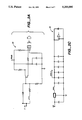
FIG. 2a is a schematic diagram of an optical transmitter according to the present invention;
FIG. 2b is a schematic diagram of an optical receiver according to the present invention;
FIG. 2c is a schematic diagram of a power supply network for the optical receiver of FIG. 2b according to the present invention;
FIG. 3 is an enlarged view of the optical transmitter of FIG. 2a;
FIG. 4 is an enlarged view of the pre-amplifier portion of the optical receiver of FIG. 2b;
FIG. 5 is an enlarged view of part of a LO-LITE circuit portion of FIG. 2b;
FIG. 6 is a diagrammatic illustration of the problem of pulse-width distortion in the prior art;
FIG. 7a is an approximate plot of the frequency-gain characteristic of a main amplifier portion of the optical receiver of FIG. 2b; and
FIG. 7b is an approximate plot of the frequency-gain characteristic of the LO-LITE circuit portion of the optical receiver of FIG. 2b.
In the description that follows, reference designations R, L, C, and so forth are used to designate resistors, inductors, capacitors and other electronic components in conventional fashion are followed by a subscript notation indicating in which of FIGS. 3-5 that component appears. For simplicity, this convention is not observed in FIGS. 3-5 themselves.
DETAILED DESCRIPTION OF THE PREFERRED EMBODIMENTS
In FIG. 2b, the first portion of an optical receiver circuitry comprises a low-noise pre-amplifier 41 and a second portion of the optical receiver circuitry comprises a main amplifier 43. The main amplifier 43 provides complementary outputs, respectively, to a signal-shaping filter 44 to produce a final electrical signal E-- OUT and to a LO-LITE circuit to produce a LO-LITE output. The pre-amplifier 41 and the LO-LITE circuit 45 will be described in greater detail in connection with FIGS. 4 and 5 hereafter.
In the optical transmitter in FIG. 3, a laser semiconductor diode is optically coupled to the end of an optical fiber and is electrically coupled by a three terminal connection 49 to the optical transmitter circuitry. The laser is driven through a current-limiting resistor R4.sub.(3) by a transistor T1.sub.(3) supplied with power through a resistor R2.sub.(3). Power is also supplied through a resistor R3.sub.(3) to reverse bias a back facet monitor (commonly a photodiode) of the semiconductor laser which may be used to perform the optical monitoring function of block 15 of FIG. 1a. In the present embodiment, however, the monitoring output otherwise available at the laser side of resistor R3.sub.(3) is not used. Capacitors C1 and C2 minimize ripple in the power supply voltage.
It should be especially noted that the optical transmitter of FIG. 3 includes a pulse conditioning network for driving the transistor T1.sub.(3). In the illustrated embodiment, the optical transmitter includes an inductor L1.sub.(3), a resistor R1.sub.(3) and a diode D1.sub.(3). When an information pulse signal is first supplied to the pulse conditioning network, a rush of current flows through the diode D1.sub.(3) to quickly turn on the transistor T1.sub.(3) and activate the laser diode. As the pulse continues, a portion of the energy of the pulse determined by resistors R1.sub.(3) and R5.sub.(3) is stored in the inductor L1.sub.(3). When the pulse subsides, the pulse energy stored in the electromagnetic field of the inductor L1.sub.(3) is released in an effort to maintain the current through the inductor. This current flows into the base of the transistor T1.sub.(3) so as to prolong activation of the laser for a time approximately equal to the turn-on time of the laser. In this manner, the above-described pulse-width distortion problem is substantially avoided.
The detector and pre-amplifier portions of the optical receiver of the present invention function to detect a series of light pulses as produced, for example, by the optical transmitter of FIG. 3, convert those pulses into a low-level electrical signal and amplify the low-level electrical signal into an intermediate level electrical signal in as noise-free a manner as possible. A PIN photo diode is used as the detector element, and is optically coupled to an optical fiber and electrically coupled to a three-terminal connector 51. The PIN photo diode is reversed biased by a resistor R1.sub.(4) connected to power. The detection output of the PIN photo diode is input to one of the gates of a dual-gate MOSFET T1.sub.(4) used to realize the first stage of the pre-amplifier. A MOSFET is chosen because of its characteristically low noise. A dual-gate MOSFET in particular is chosen so that the amplification of the first stage may be controlled using the second gate. In the present invention, the second gate is set to a potential of about 4 V by means of the resistive divider network R2.sub.(4) and R5.sub.(4) and the stabilizing capacitor C1.sub.(4). The dual-gate MOSFET is biased by resistors R3.sub.(4) and R6.sub.(4). The latter resistor is connected in shunt with a capacitor C2.sub.(4) whose value may be adjusted to adjust the frequency response of the pre-amplifier.
The output of the first dual-gate MOSFET stage is input to a second stage realized by a conventional bipolar NPN transistor T2.sub.(4) biased via resistors R4.sub.(4) and R7.sub.(4) so as to achieve an amplification of about 6 or 7. A feedback path is provided from the emitter of the transistor T2.sub.(4) to the input of the MOSFET via feedback resistor Rf. To a reasonable approximation, thermal noise in an electrical component increases linearly as the impedance of that component, as is well-known in the art. Thermal noise is the chief limiting factor of the sensitivity of the optical receiver. In accordance with the present invention, the thermal noise of the pre-amplifier is reduced by using a relatively small feedback resistor Rf (for example of approximately 1.5 kilo-ohms), at the same time biasing the second stage transistor T2.sub.(4) so as to achieve a moderate gain of about 6 or 7. As a result, approximately 10 kilo-ohms of transimpedance may be obtained with a feedback resistor of only 1.5 kilo-ohms. The output of the second stage is input to a final buffer stage realized using an NPN transistor T3.sub.(4) and associated resistor R8.sub.(4). The output of pre-amplifier portion of the optical receiver is taken at the emitter of the transistor T3.sub.(4).
Optical LANs are typically provided with a LO-LITE circuit that compares the level of a received light signal to a specified threshold to determine when the light signal is too weak to be properly received. When a LO-LITE condition is detected, the output of the optical receiver (E-- OUT in FIG. 2b) is suspended. Referring now to FIG. 5, the LO-LITE circuit of the present invention presents a very simple single-transistor circuit for LAN applications but is designed to cover a broad frequency range of 100 KHz to 16 MHz in cooperation with the pre-amplifier and the main amplifier of the optical receiver. The single transistor is a conventional NPN bipolar transistor T1.sub.(5) biased via resistors R5.sub.(5), R6.sub.(5) and R3.sub.(5). A DC blocking capacitor CB forms the input of the LO-LITE circuit and is connected to the base of the transistor T1.sub.(5). Connected to the collector of the transistor T1.sub.(5) is a diode D1.sub.(5) through which an integrator composed of the shunt combination of a capacitor C4.sub.(5) and a resistor R4.sub.(5) is charged. The output of the integrator is compared with an appropriate threshold to determine when a LO-LITE condition exists. A stabilizing capacitor C3.sub.(5) stabilizes power supply to the LO-LITE circuit.
Referring to FIG. 7a, the main amplifier of the optical receiver exhibits a frequency-gain characteristic that trails off in the vicinity of 16 MHz. To compensate for this characteristic, the LO-LITE circuit of the present invention is designed to exhibit a frequency-gain characteristic as illustrated in FIG. 7b such that the characteristic exhibits a peak B in the vicinity of 16 MHz where the characteristic of the main amplifier trails off. The lower cutoff frequency of the LO-LITE circuit occurs at a knee A portion of the characteristic in the vicinity of about 100 KHz.
Referring again to FIG. 5, two RC pairs, R1C1.sub.(5) and R2C2.sub.(5), realize two zeros, one at approximately 100 KHz to yield the knee A of the frequency-gain response of FIG. 7a and another at approximately 16 MHz to yield the peak B to compensate for gain error caused by the main amplifier. In this manner, a very simple single-transistor LO-LITE circuit is enabled to operate over a relatively wide frequency range.
The features of the present invention described above allow a fiber optic LAN having a favorable cost-performance ratio to be achieved. Using the pre-amplifier design of the present invention with its low noise figure, high receiver sensitivity may be achieved. Using the pulse compensation network of the optical transmitter of the present invention, pulse width distortion may be reduced. Finally, the LO-LITE of the circuit of the present invention provides a very simple and economical circuit that operates over a wide bandwidth.
The present invention, therefore, provides a low-cost, high-performance fiber optic LAN alternative. Still further, the present invention provides an optical receiver having a LO-LITE circuit of single-transistor construction yet operable over a wide frequency range.
The foregoing has described the principles, preferred embodiments and modes of operation of the present invention. However, the invention should not be construed as limited to the particular embodiments discussed. Instead, the above-described embodiments should be regarded as illustrative rather than restrictive, and it should be appreciated that variations may be made in those embodiments by workers skilled in the art without departing from the scope of present invention as defined by the following claims.

Claims (5)

What is claimed is:
1. An optical transmitter comprising:
an input terminal;
pulse conditioning means DC-coupled to said input terminal for receiving from said input terminal pulse energy of an input pulse to be transmitted, quickly passing a portion of the pulse energy, storing a portion of the pulse energy, and releasing a stored portion of the pulse energy as input pulse energy subsides; and
optical source means connected to the pulse conditioning means for, after a turn-on delay, beginning to emit light following initiation of said input pulse in response to the portion of the pulse energy that is quickly passed, and for, during a turn-off delay substantially equal to said turn-on delay, continuing to emit light after the subsidence of said input in response to the stored portion of the pulse energy released by the pulse conditioning means, thereby reducing pulse width distortion.
2. The optical transmitter of claim 1 wherein the pulse conditioning means comprises a shunt combination of half-wave rectifying means and electromagnetic storage means.
3. The optical transmitter of claim 2 wherein the electromagnetic energy storage means is an inductor.
4. The optical transmitter of claim 3 wherein the half-wave rectifying means is a diode.
5. The optical transmitter of claim 2 wherein the optical source means is a semiconductor laser diode.
US07/788,848 1991-11-07 1991-11-07 Digital pulse optical transmitter and receiver for local area network applications Expired - Fee Related US5253096A (en)

Priority Applications (1)

Application Number Priority Date Filing Date Title
US07/788,848 US5253096A (en) 1991-11-07 1991-11-07 Digital pulse optical transmitter and receiver for local area network applications

Applications Claiming Priority (1)

Application Number Priority Date Filing Date Title
US07/788,848 US5253096A (en) 1991-11-07 1991-11-07 Digital pulse optical transmitter and receiver for local area network applications

Publications (1)

Publication Number Publication Date
US5253096A true US5253096A (en) 1993-10-12

Family

ID=25145760

Family Applications (1)

Application Number Title Priority Date Filing Date
US07/788,848 Expired - Fee Related US5253096A (en) 1991-11-07 1991-11-07 Digital pulse optical transmitter and receiver for local area network applications

Country Status (1)

Country Link
US (1) US5253096A (en)

Cited By (7)

* Cited by examiner, † Cited by third party
Publication number Priority date Publication date Assignee Title
US5475381A (en) * 1992-01-28 1995-12-12 Servio Logic Corp. High speed infrared communications system using pulse sets
US5541759A (en) * 1995-05-09 1996-07-30 Microsym Computers, Inc. Single fiber transceiver and network
US6037841A (en) * 1997-10-07 2000-03-14 Applied Micro Circuits Corporation Impedance matched CMOS transimpedance amplifier for high-speed fiber optic communications
US20050117916A1 (en) * 2003-11-18 2005-06-02 Infineon Technologies Ag Digital optical receiving module, and a method for monitoring the signal quality of a transmitted, modulated optical signal
US7002131B1 (en) 2003-01-24 2006-02-21 Jds Uniphase Corporation Methods, systems and apparatus for measuring average received optical power
US20060245765A1 (en) * 2005-04-28 2006-11-02 Salam Elahmadi Methods of spread-pulse modulation and nonlinear time domain equalization for fiber optic communication channels
US7215883B1 (en) 2003-01-24 2007-05-08 Jds Uniphase Corporation Methods for determining the performance, status, and advanced failure of optical communication channels

Citations (3)

* Cited by examiner, † Cited by third party
Publication number Priority date Publication date Assignee Title
US3614447A (en) * 1969-06-16 1971-10-19 Bell Telephone Labor Inc Method for modulating semiconductor lasers
US4759080A (en) * 1983-11-16 1988-07-19 Nec Corporation Coherent optical communication system with FSK heterodyne or homodyne detection and little influence by distortion of a modulated optical signal
US4850046A (en) * 1986-10-30 1989-07-18 Neiman Infrared transmitter of coded message having fixed code and large number of combinations

Patent Citations (3)

* Cited by examiner, † Cited by third party
Publication number Priority date Publication date Assignee Title
US3614447A (en) * 1969-06-16 1971-10-19 Bell Telephone Labor Inc Method for modulating semiconductor lasers
US4759080A (en) * 1983-11-16 1988-07-19 Nec Corporation Coherent optical communication system with FSK heterodyne or homodyne detection and little influence by distortion of a modulated optical signal
US4850046A (en) * 1986-10-30 1989-07-18 Neiman Infrared transmitter of coded message having fixed code and large number of combinations

Cited By (15)

* Cited by examiner, † Cited by third party
Publication number Priority date Publication date Assignee Title
US5475381A (en) * 1992-01-28 1995-12-12 Servio Logic Corp. High speed infrared communications system using pulse sets
US5659299A (en) * 1992-01-28 1997-08-19 Servio Logic Corporation High speed infrared communications system using pulse sets
US5541759A (en) * 1995-05-09 1996-07-30 Microsym Computers, Inc. Single fiber transceiver and network
US6037841A (en) * 1997-10-07 2000-03-14 Applied Micro Circuits Corporation Impedance matched CMOS transimpedance amplifier for high-speed fiber optic communications
US6275114B1 (en) 1997-10-07 2001-08-14 Applied Micro Circuits Corporation Impedance matched CMOS transimpedance amplifier for high-speed fiber optic communications
US7002131B1 (en) 2003-01-24 2006-02-21 Jds Uniphase Corporation Methods, systems and apparatus for measuring average received optical power
US7215883B1 (en) 2003-01-24 2007-05-08 Jds Uniphase Corporation Methods for determining the performance, status, and advanced failure of optical communication channels
US20050117916A1 (en) * 2003-11-18 2005-06-02 Infineon Technologies Ag Digital optical receiving module, and a method for monitoring the signal quality of a transmitted, modulated optical signal
US8750725B2 (en) * 2003-11-18 2014-06-10 Finisar Corporation Digital optical receiving module, and a method for monitoring the signal quality of a transmitted, modulated optical signal
US20060245765A1 (en) * 2005-04-28 2006-11-02 Salam Elahmadi Methods of spread-pulse modulation and nonlinear time domain equalization for fiber optic communication channels
US20060245758A1 (en) * 2005-04-28 2006-11-02 Salam Elahmadi Systems with spread-pulse modulation and nonlinear time domain equalization for fiber optic communication channels
US20060245757A1 (en) * 2005-04-28 2006-11-02 Salam Elahmadi Apparatus with spread-pulse modulation and nonlinear time domain equalization for fiber optic communication channels
US7286762B2 (en) 2005-04-28 2007-10-23 Menara Networks Apparatus with spread-pulse modulation and nonlinear time domain equalization for fiber optic communication channels
US7302192B2 (en) 2005-04-28 2007-11-27 Menara Networks Methods of spread-pulse modulation and nonlinear time domain equalization for fiber optic communication channels
US7715731B2 (en) 2005-04-28 2010-05-11 Menara Networks Systems with spread-pulse modulation and nonlinear time domain equalization for fiber optic communication channels

Similar Documents

Publication Publication Date Title
US5532471A (en) Optical transimpedance amplifier with high dynamic range
KR100900205B1 (en) Wide dynamic range transimpedance amplifier
EP0108792B1 (en) Fet amplifier with wide dynamic range
EP0597632B1 (en) Packet mode digital data receiver
US4415803A (en) Optical receiver with improved dynamic range
EP0597633A1 (en) Burst mode digital data receiver
JP2690129B2 (en) Method and structure for increasing the dynamic range in the input stage of an optical receiver
JPH06177664A (en) Digital photoreception circuit, trans-impedance amplifier circuit and preamplifier circuit
US6778021B2 (en) Wide dynamic range transimpedance amplifier with a controlled low frequency cutoff at high optical power
JPS59216339A (en) Light receiver and light transmission system
CA2128894A1 (en) Optical receiver
US4075576A (en) Sensitive high speed solid state preamp
US6359517B1 (en) Photodiode transimpedance circuit
US4608542A (en) Bandwidth controlled data amplifier
US5111324A (en) Optical receivers
JP2010093353A (en) Optical receiver
JPH0783313B2 (en) Front end for broadband optical receiver
US5253096A (en) Digital pulse optical transmitter and receiver for local area network applications
US4295225A (en) Fiber optic repeater
US6535308B1 (en) Method and apparatus for converting electrical signals and optical signals for bidirectional communication over a single optical fiber
US6819722B2 (en) Offset control circuit, optical receiver using the same and optical communication system
CA2480608A1 (en) Elevated front-end transimpedance amplifier
JP3021913B2 (en) Optical receiver
JPH04225630A (en) Wide dynamic range optical receiver
US5561383A (en) Switchable peak/average detect circuit

Legal Events

Date Code Title Description
AS Assignment

Owner name: RAYLAN CORPORATION, CALIFORNIA

Free format text: ASSIGNMENT OF ASSIGNORS INTEREST.;ASSIGNORS:FREEMAN, WILLIAM R.;PATEL, BHAVESH;REEL/FRAME:005914/0893

Effective date: 19911028

FEPP Fee payment procedure

Free format text: PAYER NUMBER DE-ASSIGNED (ORIGINAL EVENT CODE: RMPN); ENTITY STATUS OF PATENT OWNER: LARGE ENTITY

Free format text: PAYOR NUMBER ASSIGNED (ORIGINAL EVENT CODE: ASPN); ENTITY STATUS OF PATENT OWNER: LARGE ENTITY

FEPP Fee payment procedure

Free format text: PAT HLDR NO LONGER CLAIMS SMALL ENT STAT AS SMALL BUSINESS (ORIGINAL EVENT CODE: LSM2); ENTITY STATUS OF PATENT OWNER: LARGE ENTITY

FPAY Fee payment

Year of fee payment: 4

FPAY Fee payment

Year of fee payment: 8

REMI Maintenance fee reminder mailed
LAPS Lapse for failure to pay maintenance fees
STCH Information on status: patent discontinuation

Free format text: PATENT EXPIRED DUE TO NONPAYMENT OF MAINTENANCE FEES UNDER 37 CFR 1.362

FP Lapsed due to failure to pay maintenance fee

Effective date: 20051012