US5250856A - Differential input buffer-inverters and gates - Google Patents
Differential input buffer-inverters and gates Download PDFInfo
- Publication number
- US5250856A US5250856A US07/863,551 US86355191A US5250856A US 5250856 A US5250856 A US 5250856A US 86355191 A US86355191 A US 86355191A US 5250856 A US5250856 A US 5250856A
- Authority
- US
- United States
- Prior art keywords
- coupled
- transistor
- emitter
- bipolar
- mos
- Prior art date
- Legal status (The legal status is an assumption and is not a legal conclusion. Google has not performed a legal analysis and makes no representation as to the accuracy of the status listed.)
- Expired - Lifetime
Links
Images


Classifications
-
- H—ELECTRICITY
- H03—ELECTRONIC CIRCUITRY
- H03K—PULSE TECHNIQUE
- H03K19/00—Logic circuits, i.e. having at least two inputs acting on one output; Inverting circuits
- H03K19/02—Logic circuits, i.e. having at least two inputs acting on one output; Inverting circuits using specified components
- H03K19/08—Logic circuits, i.e. having at least two inputs acting on one output; Inverting circuits using specified components using semiconductor devices
- H03K19/094—Logic circuits, i.e. having at least two inputs acting on one output; Inverting circuits using specified components using semiconductor devices using field-effect transistors
- H03K19/0944—Logic circuits, i.e. having at least two inputs acting on one output; Inverting circuits using specified components using semiconductor devices using field-effect transistors using MOSFET or insulated gate field-effect transistors, i.e. IGFET
- H03K19/09448—Logic circuits, i.e. having at least two inputs acting on one output; Inverting circuits using specified components using semiconductor devices using field-effect transistors using MOSFET or insulated gate field-effect transistors, i.e. IGFET in combination with bipolar transistors [BIMOS]
-
- H—ELECTRICITY
- H03—ELECTRONIC CIRCUITRY
- H03K—PULSE TECHNIQUE
- H03K19/00—Logic circuits, i.e. having at least two inputs acting on one output; Inverting circuits
- H03K19/0175—Coupling arrangements; Interface arrangements
- H03K19/017509—Interface arrangements
- H03K19/017518—Interface arrangements using a combination of bipolar and field effect transistors [BIFET]
- H03K19/017527—Interface arrangements using a combination of bipolar and field effect transistors [BIFET] with at least one differential stage
Definitions
- the present invention relates to devices utilizing bipolar and field effect transistors (FETs). More particularly, the present invention relates to BiCMOS buffers, inverters, and gates which utilize differential inputs and provide increased output drive at a buffered output.
- FETs bipolar and field effect transistors
- BiCMOS which utilizes both bipolar and CMOS transistors in a single device has been increasingly explored in the past few years.
- the advantage of BiCMOS circuits over conventional CMOS or bipolar circuits is that the high speed characteristic of bipolar circuits can be obtained with an integration density and low power consumption characteristic of CMOS circuits.
- Typical of BiCMOS buffers, inverters and gates known in the art are the following patents and disclosures: U.S. Pat. No. 4,558,234 to Suzuki et al.; U.S. Pat. No. 4,638,186 to McLaughlin; U.S. Pat. No. 4,649,294 to McLaughlin; U.S. Pat. No. 4,733,110 to Hara et al.; EPO Publication 0212004; IBM TDB Vol. 29, #3, August 1986, p.1191-1192; Japanese Patent Publication (JPP) 62-26691 to Miyaoka et al; JPP 62-230221 to Ueno; and JPP 61-274512 to Nakamura.
- JPP Japanese Patent Publication
- non-synchronous differential input is typically provided via use of one or more inverters which slows the circuit and causes the differential input to have phase disparity.
- each circuit of the invention contains a pair of bipolar transistors and an MOS transistor.
- One of the bipolar transistors has a base responsive to the noninverting input of a differential input, a collector coupled to a first voltage reference rail, and an emitter.
- the other bipolar transistor has a base, a collector coupled to the emitter of the first-mentioned bipolar transistor, and an emitter coupled to a second voltage rail.
- the MOS transistor has a gate electrode responsive to the inverting input of the differential input, a drain coupled to the emitter of the first bipolar transistor, and a source coupled to the base of the second-mentioned bipolar transistor.
- a circuit output is available at a node coupled to the emitter of the first bipolar transistor.
- the noninverting and inverting inputs are normally substantially synchronous and are provided from an input circuit which may take many forms.
- the two bipolar transistors are npn devices, and the MOS transistor is an nMOS FET.
- the first and second rails respectively are high and low voltage rails.
- Some of the preceding embodiments include a further MOS transistor of opposite MOS type--i.e., complementary--to the first-mentioned MOS transistor.
- the further MOS transistor has a gate electrode, a source coupled to the first rail, and a drain coupled to the emitter of the first bipolar transistor.
- the gate electrode of the further MOS device is responsive to the inverted input, sometimes via the base-emitter junction of another bipolar transistor.
- the further MOS transistor acts to pull the circuit output to the voltage of the first rail when the first transistor turns on and thereby avoids the 1-Vbe reduction in output voltage drive that would otherwise normally occur. Consequently, the circuit is cascadable.
- Additional embodiments include the aforementioned circuitry plus duplicative circuitry which is arranged such that the noninverted input signal is received at the gate electrodes and bases of transistors corresponding to transistors where the inverted input signal is received by the aforementioned circuitry, and vice versa.
- a differential output is obtained, with the noninverting output signal obtained from the emitter of a bipolar transistor of the "original" circuit, and the inverting output signal obtained from the emitter of a bipolar transistor of the duplicative circuit.
- npn transistors can be replaced with pnp transistors; in which case the polarities of the nMOS and pMOS devices are reversed along with the polarities of the voltage rails.
- the duplicative circuitry can employ transistors of opposite polarity to the original circuitry.
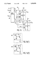
- FIGS. 1a and 1b are circuit diagrams of differential input BiCMOS buffers having a single ended output and a differential output respectively.
- FIGS. 1a(1) and 1a(2) are circuit diagrams for alternative versions of the circuitry shown in phantom in FIG. 1a.
- FIGS. 1b(1) and 1b(2) are circuit diagrams for an alternative version of the circuitry shown in phantom in FIG. 1b.
- FIGS. 2a and 2b are circuit diagrams of cascadable differential input BiCMOS bufffers having a single ended output and a differential output respectively.
- FIG. 3 is a circuit diagram of a cascadable differential input, differential output BiCMOS buffer/inverter
- FIG. 4 is a circuit diagram of another cascadable differential input, differential output BiCMOS buffer/inverter
- FIGS. 5a and 5b are circuit diagrams of differential two-input BiCMOS gates having a single output (OR/NAND) and a differential output (OR/NAND, NOR/AND) respectively;
- FIG. 6 is a circuit diagram of a differential two-input BiCMOS gate having two single ended outputs.
- BiCMOS Bipolar transistors and FETs, regardless of whether MOSFETs or other types of IGFETs are used or whether both p-channel and n-channel type MOS transistors are utilized in a single circuit.
- any description of a transistor as a MOS transistor is intended to be understood in its broadest sense to include other types of IGFETs and not to be limited to metal-gate FETs.
- circuits are described as preferably including npn bipolar transistors, if the polarities of the bipolar and MOS transistors are reversed, equivalent functional circuits are obtained. Further, it will be appreciated that while “inputs” and “outputs" to and from the circuit are described, little distinction is provided regarding whether the inputs or outputs are signals or nodes, as those skilled in the art will readily appreciate whether a signal or node is being described.
- FIGS. 1a and 1b respectively show buffer circuits 10a and 10b, where like parts are coded with like reference numbers.
- the elements in FIG. 1a are further coded with the designation "a”, while the corresponding elements in FIG. 1b are further coded with the designation "b-1”.
- the duplicate elements in FIG. 1b are further coded with the designation "b-2".
- the designations "a”, “b-1” and “b-2" are dropped in the following discussion when FIGS. 1a and 1b are described together.
- buffer circuit 10 in the two figures contains an input circuit 11 that receives one or both of complementary voltages V 0 and V 0 on lines 13 and 15.
- Input circuit 11 provides therefrom over lines 17 and 19 a synchronous differential signal with noninverting signal V in and inverting signal V in (the terms “noninverting” and “inverting” being terms relative to each other only).
- the input circuit 11 may take many forms, provided the signals it outputs over lines 17 and 19 comprise a substantially synchronous differential signal.
- input circuit 11 may be a RAM with dual output ports which are identically clocked.
- input circuit 11 may include an inverter from which the inverting signal is obtained, in conjunction with a parallel pass gate which introduces identical delay to the noninverted signal.
- the noninverting signal V in of the differential input signal is provided to the base of the npn bipolar transistor 20a, which has its collector connected to the high voltage rail V HH .
- the noninverting signal V in is also provided to the gate electrode of nMOS transistor 24a which has its source coupled to the low voltage rail V LL .
- the inverted signal V in is provided to the gate of nMOS transistor 22a which has its source coupled to the drain of transistor 24a, and its drain coupled to the emitter of bipolar transistor 20a.
- a second bipolar transistor 28a has its collector coupled to the emitter of bipolar transistor 20a, its emitter coupled to the source of nMOS transistor 24a, and its base coupled to the drain of transistor 24a and the source of transistor 22a.
- the emitter of transistor 20a, the collector of transistor 28a and the drain of MOS transistor 22a are all connected together through a node from which the output V out of buffer circuit 10a is taken.
- the high signal at the base of bipolar transistor 20a quickly turns it on and pulls up the output voltage V out to V in -V be where V be is the typical base-emitter voltage drop for a conducting bipolar transistor.
- the high signal is fed to nMOS transistor 24a which turns on.
- transistor 24a When transistor 24a is turned on, it brings its drain voltage down to the voltage at its source. Thus, the voltage at the drain of transistor 24a is brought low (i.e., to the voltage V LL ), and hence the voltage at the base of bipolar transistor 28a is not sufficient to turn bipolar transistor 28a on.
- the arrangement with bipolar transistors 20a and 28a has its voltage output controlled by transistors 20a and 28a depending on the input values V in and V in .
- V in When V in is high, transistor 20a is on and pulls the voltage output high, while when V in is high, transistor 28a is on and pulls the voltage output low.
- nMOS transistor 24a can be replaced with a resistor 29a connected between the base of npn transistor 28a and the low voltage rail V LL .
- Transistor 24a can also be deleted from the buffer. See FIG. 1a(2).
- FIG. 1b further includes a duplicate 20b of the circuit 10b with reversed inputs which provides an inverted output V out .
- the input V in is fed to npn bipolar transistor 20b-1 and nMOS transistor 24b-1, as well as nMOS transistor 22b-2.
- the input V in is fed to nMOS transistor 22b-1, as well as to bipolar transistor 20b-2 and nMOS transistor 24b-2.
- a differential output with noninverting output V out and inverting output V out is taken from the emitters of transistors 20b-1 and 20b-2. This differential output is synchronous, buffered and suffers a delay of only one transistor delay.
- transistors 24b-1 and 24b-2 can be replaced with resistors. See FIGS. 1b(1) and 1b(2) where these resistors are shown as items 29b-1 and 29b-2.
- buffer circuits of FIGS. 1a and 1b may act as inverters as well as buffers simply by reversing the polarities of inputs V in and V in .
- FIGS. 2a and 2b provide second embodiments of buffers/inverters which are very similar to those of FIGS. 1a and 1b, and where like parts are indicated by providing FIGS. 2a and 2b with numerals one hundred removed from their counterparts in FIGS. 1a and 1b.
- Buffer 110a in FIG. 2a receives a synchronous differential input signal (V in , V in ) from input circuit 111a.
- Buffer 110a includes npn bipolar transistors 120a and 128a, and MOS transistors 122a and 124a in the same configuration of like transistors of FIG. 1a. The only difference between the buffer of FIG. 2a and that of FIG.
- Transistor 126a has its source connected to the collector of transistor 120a, its drain connected to the emitter of transistor 120a, and its gate electrode connected to the inverting input V in .
- bipolar transistor 120a When input V in is high and input V in low, bipolar transistor 120a turns on quickly, while pMOS transistor 126a turns on a little more slowly. Because the source of transistor 126a is connected to the high voltage rail, transistor 126a pulls the voltage at its drain from V in -V be (which is the voltage at the emitter of transistor 120a when the V.sub. in input is at the high input voltage V in ) all the way up to V HH . Because the output voltage swings all the way up to V HH , the circuits of FIGS. 2a and 2b can be used in series without a progressive degradation in the high output voltage. The circuits of FIGS. 2a and 2b can be used with the resistor 29 shown in FIGS. 1a(1), 1b(1), and 1b(2) to achieve rail to rail switching which eliminates leakage currents associated with partial input transitions driving CMOS gates.
- FIG. 3 a third embodiment of a differential buffer/inverter is provided.
- an input circuit 211 receives voltages V 0 and V 0 on lines 213 and 215 and provides a synchronous differential output over lines 217 and 219 with the noninverting signal V in , and the inverting signal V in .
- the V in signal from circuit 211 serves as the noninverting input into buffer 210 and is fed to the base of bipolar transistor 220-1.
- Bipolar transistor 220-1 has a collector coupled to the high voltage rail, and an emitter coupled to the noninverting output of the buffer circuit.
- transistor 220-1 Coupled to transistor 220-1 is a pMOS transistor 261-1 with its drain coupled to the collector of transistor 220-1 and its source coupled to the emitter of transistor 220-1. Also coupled to the emitter of transistor 220-1 is the drain of nMOS transistor 263-1. Transistor 263-1 is provided with the inverting input V in at its gate electrode, and has its source coupled to the low voltage rail. Noninverting output V out is taken from a node between the emitter of transistor 220-1 and the drain of transistor 263-1.
- Buffer 210 also includes another set (i.e. duplicative set) of transistors, including bipolar transistor 220-2, pMOS transistor 261-2, and nMOS transistor 263-2.
- the base of transistor 220-2 is coupled to the inverted input V in , while the collector of transistor 220-2 is coupled to the high voltage rail.
- Transistor 261-2 has its source coupled to the collector of transistor 220-2 and its drain coupled to the emitter of transistor 220-2.
- the gate electrode of transistor 261-2 is coupled to the emitter of transistor 220-1 and the drain of transistor 261-1, while the emitter of transistor 220-2 and drain of transistor 261-2 are coupled to the gate electrode of transistor 261-1.
- Transistor 263-2 is provided with input V in at its gate.
- transistor 220-1 when V in is high (V in low), transistor 220-1 turns on quickly and pulls the noninverting output V out to V in -V be .
- transistor 263-2 turns on, pulling its drain, and the gate electrode of pMOS transistor 261-1, to V LL .
- pMOS transistor 261-1 turns on and pulls output V out up to V HH , much in the same way as described above with reference to FIGS. 2a and 2b.
- transistor 263-2 is turned on, pulling its drain and hence the inverting output V out of the differential output low to the voltage V LL at its source.
- transistor 261-2 Since the source of transistor 261-2 is coupled to the emitter of transistor 220-1, transistor 261-2 turns on and pulls the voltage at the emitter of transistor 220-2 (and hence at the inverting output V out ) up to V HH . Thus, the outputs V out and V out are inverted from when V in is high and V in is low.
- the buffer/inverter embodiment of FIG. 4 combines aspects of the buffer/inverters of FIGS. 2b and 3, and is hereinafter described with like parts indicated by numbers one hundred and two hundred removed from their counterparts.
- the buffer/inverter 310 of FIG. 4 includes the bipolar transistors 320-1 and 320-2 whose bases are coupled to the inputs V in and V in , and pMOS transistors 361-1 and 361-2 which are coupled to the bipolar transistors 320-1 and 320-2 in the way shown in FIG. 3 and which provide the same features discussed above with reference to FIG. 3. Further, buffer 310 has additional npn bipolar transistors 328-1 and 328-2, and additional nMOS transistors 322-1, 322-2, 324-1, and 324-2.
- bipolar transistor 320-1 When V in goes high (V in low), bipolar transistor 320-1 turns on and bipolar transistor 320-2 turns off, MOS transistors 324-1 and 322-2 turn on, and MOS transistors 322-1 and 324-2 turn off.
- MOS transistor 324-1 turning on, bipolar transistor 328-1 is off.
- bipolar transistor 328-1 off and bipolar transistor 320-1 on With bipolar transistor 328-1 off and bipolar transistor 320-1 on, the noninverting output V out is brought high to V in -V be .
- bipolar transistor 328-2 With MOS transistor 322-2 on and MOS transistor 324-2 off, bipolar transistor 328-2 is turned on. With bipolar transistor 328-2 on and bipolar transistor 320-2 off, the inverting output V out is brought low to V LL +V be .
- pMOS transistor 361-1 With the voltage at the collector of transistor 328-2 coupled to the gate electrode of pMOS transistor 361-1 and being low, pMOS transistor 361-1 turns on and boosts the noninverting output V out up to V HH . Similarly, the high voltage output of V out is coupled to the gate of pMOS transistor 361-2 thereby keeping transistor 361-2 off and the voltage at the inverting output V out low.
- bipolar transistor 328-1 pulls the noninverting output V out low, while bipolar transistor 320-2, and then pMOS transistor 361-2, pulls the inverting output V out high.
- the buffers of FIGS. 2b, 3 and 4 are all candidates for cascading; i.e., the differential output of each may be fed as a differential input to any other differential input buffer including those buffers of FIGS. 1a, 1b, and 2a, as well as those of the art.
- cascading of buffers is desirable for providing an extremely fast delay line, with taps taken from the output of each stage. In such a situation it is preferable that each of the cascaded buffers be identical.
- increased drive is obtained by cascading buffers in a "tree" arrangement, with the outputs of a first buffer being fed as inputs to a plurality of parallel buffers.
- FIG. 5a it shows an OR/AND gate 410a that responds (1) to a first differential input formed with a noninverting input V ina and an inverting input V ina and (2) to a second differential input formed with a noninverting input V inb and an inverting input V inb .
- OR/NAND gate 410a is related to the buffer of FIG. 1a.
- npn bipolar transistors 420a and 428a as well as nMOS transistors 422a and 424a are provided.
- the collector of transistor 420a is coupled to the high voltage rail
- the base is coupled to the input signal V ina
- the emitter is coupled to the collector of transistor 428a.
- OR gate 410a includes an npn bipolar transistor 491a, and two nMOS transistors 493a and 495a. Bipolar transistor 491a is coupled in parallel with transistor 420a, except that its base is coupled to the noninverting input V inb of the second differential input.
- MOS transistor 493a is provided with its gate electrode coupled to the inverting input V inb , and with a drain coupled to the emitter of transistor 420a (via transistor 422a) and a source coupled to the drain of MOS transistor 424a.
- MOS transistor 495a is coupled in parallel with MOS transistor 424a, except that its gate is coupled to the noninverting V inb input.
- transistors 420a, 491a, 424a, and 495a turn off, while transistors 493a and 422a turn on.
- transistors 491a and 424a off, and transistors 493a and 422a on bipolar transistor 428a turns on. With transistor 428a on, and transistors 420a and 491a off, the output V out is pulled low.
- OR gate 410a functions equivalently as a NAND gate in accord with DeMorgan's theorem by reversing the V ina input with the V ina input, and the V inb input with the V inb input.
- FIG. 5b A differential output embodiment of the OR/NAND gate of FIG. 5a is seen in FIG. 5b where differential inputs V ina , V ina , and V inb , V inb are provided on lines 417bA, 419bA, and 417bB and 419bB, and npn transistors 420b-1, 428b-1, 491b-1 and 491b-1 and nMOS transistors 420b-1, 422b-1, 424b-1, 493b-1, and 495b-1 function identically as their equivalents in FIG. 5a to provide an OR/NAND function at the noninverted output V out .
- pnp transistors 420b-2, 428b-2, and 491b-2, and pMOS transistors 420b-2, 422b-2, 424b-2, 493b-2 and 495b-2 are provided and produce a NOR/AND output at the inverted output V out of the differential output.
- the pnp and pMOS transistors of the -2 section of the circuit are arranged identically to the npn and nMOS transistors of the -1 stage, except that the polarity of the inputs 417bA, 419bA, 417bB and 419bB, and the polarity of the voltage rails are reversed.
- V ina and V inb when one (or both) of V ina and V inb are high, one or both of V ina and V inb are low, and therefore, one or both of pnp transistors 420b-2, and 491b-2 (and correspondingly pMOS transistors 424b-2 and 495b-2) are turned on. With one or both of transistors 420b-2 and 491b-2 on, the inverted output V out is pulled low (i.e. to V in +V be ). Also, with one or both of transistors 424b-2 and 495b-2 on, the voltage at the base of transistor 428b-2 is brought high, and transistor 428b-2 is kept off such that it does not attempt to pull the voltage at the inverted output high.
- both V ina and V inb are low, both V ina and V inb are high, and pnp transistors 420b-2, 491b-2, 424b-2 and 495b-2 turn off, while pMOS transistors 422b-2 and 493 b-2 turn on. With transistors 422b-2 and 493b-2 on, and 424b-2 and 495b-2 off, pnp transistor 428b-2 turns on. With pnp transistor 428b-2 on, and transistors 420b-2 and 491b-2 off, the inverted output V out is pulled high.
- V out is high only when V ina and V inb are low, and is low when either V ina or V inb is high; a classical NOR gate.
- the noninverted output which is changed from an OR function to a NAND function, by reversing the V ina and V ina inputs 417bA and 419bA and V inb and V inb inputs 417bB and 419bB, the inverted output V out is changed from a NOR to an AND function with such a reversal.
- the logic gate of FIG. 6 incorporates the circuitry of FIG. 5a, along with duplicative circuitry which receives inverted inputs and which provides a second single ended output V out' .
- the second single ended output V out' does not together with the first output V out provide a differential output, as the second single ended output is not the inverse of the first single ended output
- the OR gate of FIG. 5a is set forth with bipolar transistors 520a, 528a, and 591a, and with nMOS transistors 522a, 524a, 593a, and 595a. Also, duplicative bipolar transistors 520b, 528b, and 591b, and nMOS transistors 522b, 524b, 593b, and 595b are provided. As indicated above in the discussion regarding FIG. 5a, an OR function is provided at the emitters of transistors 520a and 591a. Also, as indicated above in the discussion regarding FIG.
- differential input BiCMOS buffer inverters, and gates. While particular embodiments have been described, it is not intended that the invention be limited thereto as it is intended that the invention be broad in scope as the art will allow.
- nMOS transistor is used in most of the buffer and inverter embodiments to cause the base of the lower bipolar transistor of the two bipolar transistor arrangement to quickly reach the voltage of the low voltage rail (i.e., a hard pull off the base)
- a resistor could be substituted for that nMOS transistor in the embodiments of FIGS. 4-6 as described above for the circuitry of FIGS. 1a-2b.
- that transistor can be eliminated entirely from the circuit as shown in FIGS. 1a(2), although current leakage could result.
- gates having as many differential inputs as desired can be constructed by providing additional bipolar transistors with bases connected to additional (inputs - e.g., "V inc " and "V ind -") in parallel with the bipolar transistors having the V ina and V inb input signals connected to their bases, by providing additional MOS transistors with inverting V inc and V ind gate inputs in series with the MOS transistors having the V ina and V inb inputs to their gates, and by further providing additional MOS transistors with V inc and V ind gate inputs in parallel with the parallel MOS transistors with V ina and V inb gate inputs.
- npn bipolar transistors were disclosed in conjunction with advantageous location of nMOS and pMOS transistors, it will be appreciated that pnp bipolar transistors as well as substitution of pMOS for nMOS transistors and vice versa could be effectively utilized with minor changes which would be apparent to those skilled in the art. Therefore, it will be appreciated by those skilled in the art that yet other modifications could be made to the provided invention without deviating from its spirit and scope as so claimed.
Landscapes
- Engineering & Computer Science (AREA)
- Computer Hardware Design (AREA)
- Physics & Mathematics (AREA)
- Computing Systems (AREA)
- General Engineering & Computer Science (AREA)
- Mathematical Physics (AREA)
- Power Engineering (AREA)
- Logic Circuits (AREA)
Abstract
Description
Claims (39)
Priority Applications (1)
| Application Number | Priority Date | Filing Date | Title |
|---|---|---|---|
| US07/863,551 US5250856A (en) | 1989-12-28 | 1991-07-01 | Differential input buffer-inverters and gates |
Applications Claiming Priority (2)
| Application Number | Priority Date | Filing Date | Title |
|---|---|---|---|
| US45821789A | 1989-12-28 | 1989-12-28 | |
| US07/863,551 US5250856A (en) | 1989-12-28 | 1991-07-01 | Differential input buffer-inverters and gates |
Related Parent Applications (1)
| Application Number | Title | Priority Date | Filing Date |
|---|---|---|---|
| US45821789A Continuation | 1989-12-28 | 1989-12-28 |
Publications (1)
| Publication Number | Publication Date |
|---|---|
| US5250856A true US5250856A (en) | 1993-10-05 |
Family
ID=27038904
Family Applications (1)
| Application Number | Title | Priority Date | Filing Date |
|---|---|---|---|
| US07/863,551 Expired - Lifetime US5250856A (en) | 1989-12-28 | 1991-07-01 | Differential input buffer-inverters and gates |
Country Status (1)
| Country | Link |
|---|---|
| US (1) | US5250856A (en) |
Cited By (17)
| Publication number | Priority date | Publication date | Assignee | Title |
|---|---|---|---|---|
| US5382842A (en) * | 1992-05-29 | 1995-01-17 | Nec Corporation | Composite logic circuit with bipolar transistor-complementary field effect transistor |
| US5410267A (en) * | 1993-09-24 | 1995-04-25 | Intel Corporation | 3.3 V to 5 V supply interface buffer |
| US5422523A (en) * | 1992-11-09 | 1995-06-06 | Intel Corporation | Apparatus for translating logic signal levels from 3.3 volts to 5 volts |
| US5538908A (en) * | 1995-04-27 | 1996-07-23 | Lg Semicon Co., Ltd. | Method for manufacturing a BiCMOS semiconductor device |
| US5592142A (en) * | 1995-09-15 | 1997-01-07 | International Business Machines Corporation | High speed greater than or equal to compare circuit |
| US5757873A (en) * | 1995-01-20 | 1998-05-26 | Lsi Logic Corporation | Differential delay buffer |
| US5848101A (en) * | 1996-01-25 | 1998-12-08 | Cirrus Logic, Inc. | Circuits systems and methods for reducing power loss during transfer of data across an I/O bus |
| US5920729A (en) * | 1996-04-30 | 1999-07-06 | Vtc Inc. | Apparatus for providing pair of complementary outputs with first and subcircuits to convert non-complementary and complementary inputs to first and second pair of complementary output |
| US6215330B1 (en) | 1999-06-11 | 2001-04-10 | Trw Inc. | Differential diode transistor logic (DDTL) circuit enhancements |
| US20040098231A1 (en) * | 1998-05-14 | 2004-05-20 | Chandler Van S. | Zero dead time architecture and method for flow cytometer |
| US20060156050A1 (en) * | 2005-12-23 | 2006-07-13 | Institute Of Computer Science, Foundation For Research And Technology - Hellas ("Ics") | System and method of determining the speed of digital application specific integrated circuits |
| US20060190852A1 (en) * | 2005-01-12 | 2006-08-24 | Sotiriou Christos P | Asynchronous, multi-rail, asymmetric-phase, static digital logic with completion detection and method for designing the same |
| US20060217919A1 (en) * | 2005-01-12 | 2006-09-28 | Institute Of Computer Science, Foundation For Research And Technology - Hellas ("Ics") | System and method of determining the speed of digital application specific integrated circuits |
| US7355450B1 (en) | 2005-05-27 | 2008-04-08 | Altera Corporation | Differential input buffers for low power supply |
| US20080288203A1 (en) * | 2005-01-12 | 2008-11-20 | Sotiriou Christos P | System and method of determining the speed of digital application specific integrated circuits |
| US20090167380A1 (en) * | 2007-12-26 | 2009-07-02 | Sotiriou Christos P | System and method for reducing EME emissions in digital desynchronized circuits |
| US20150371705A1 (en) * | 2013-01-30 | 2015-12-24 | Commissariat a l'énergie atomique et aux énergies alternatives | Method for programming a bipolar resistive switching memory device |
Citations (16)
| Publication number | Priority date | Publication date | Assignee | Title |
|---|---|---|---|---|
| US4301383A (en) * | 1979-10-05 | 1981-11-17 | Harris Corporation | Complementary IGFET buffer with improved bipolar output |
| US4558234A (en) * | 1981-02-25 | 1985-12-10 | Tokyo Shibaura Denki Kabushiki Kaisha | Complementary MOSFET logic circuit |
| US4616146A (en) * | 1984-09-04 | 1986-10-07 | Motorola, Inc. | BI-CMOS driver circuit |
| JPS61274512A (en) * | 1985-05-30 | 1986-12-04 | Oki Electric Ind Co Ltd | Output buffer circuit |
| US4638186A (en) * | 1985-12-02 | 1987-01-20 | Motorola, Inc. | BIMOS logic gate |
| JPS6226691A (en) * | 1985-07-26 | 1987-02-04 | Hitachi Ltd | Semiconductor integrated circuit device |
| JPS6230221A (en) * | 1985-07-31 | 1987-02-09 | Nippon Seiki Co Ltd | Liquid crystal display element |
| EP0212004A2 (en) * | 1985-07-01 | 1987-03-04 | Kabushiki Kaisha Toshiba | A solid state inverting circuit having a bipolar transistor for rapidly processing I/O signals |
| US4649294A (en) * | 1986-01-13 | 1987-03-10 | Motorola, Inc. | BIMOS logic gate |
| US4733110A (en) * | 1986-03-22 | 1988-03-22 | Kabushiki Kaisha Toshiba | BICMOS logical circuits |
| US4769561A (en) * | 1983-12-12 | 1988-09-06 | Hitachi, Ltd. | Bipolar transistor-field effect transistor composite circuit |
| US4783604A (en) * | 1986-03-31 | 1988-11-08 | Kabushiki Kaisha Toshiba | Buffer circuit for outputting signals of different polarities |
| US4804869A (en) * | 1987-03-27 | 1989-02-14 | Kabushiki Kaisha Toshiba | BiMOS logical circuit |
| US4883988A (en) * | 1985-12-27 | 1989-11-28 | Hitachi, Ltd. | Current mirror switching circuit |
| US4883979A (en) * | 1988-02-16 | 1989-11-28 | Texas Instruments Incorporated | Darlington BiCMOS driver circuit |
| EP0398808A2 (en) * | 1989-05-17 | 1990-11-22 | Fujitsu Limited | Level conversion circuit for converting elc-level signal into ttl-level signal |
-
1991
- 1991-07-01 US US07/863,551 patent/US5250856A/en not_active Expired - Lifetime
Patent Citations (16)
| Publication number | Priority date | Publication date | Assignee | Title |
|---|---|---|---|---|
| US4301383A (en) * | 1979-10-05 | 1981-11-17 | Harris Corporation | Complementary IGFET buffer with improved bipolar output |
| US4558234A (en) * | 1981-02-25 | 1985-12-10 | Tokyo Shibaura Denki Kabushiki Kaisha | Complementary MOSFET logic circuit |
| US4769561A (en) * | 1983-12-12 | 1988-09-06 | Hitachi, Ltd. | Bipolar transistor-field effect transistor composite circuit |
| US4616146A (en) * | 1984-09-04 | 1986-10-07 | Motorola, Inc. | BI-CMOS driver circuit |
| JPS61274512A (en) * | 1985-05-30 | 1986-12-04 | Oki Electric Ind Co Ltd | Output buffer circuit |
| EP0212004A2 (en) * | 1985-07-01 | 1987-03-04 | Kabushiki Kaisha Toshiba | A solid state inverting circuit having a bipolar transistor for rapidly processing I/O signals |
| JPS6226691A (en) * | 1985-07-26 | 1987-02-04 | Hitachi Ltd | Semiconductor integrated circuit device |
| JPS6230221A (en) * | 1985-07-31 | 1987-02-09 | Nippon Seiki Co Ltd | Liquid crystal display element |
| US4638186A (en) * | 1985-12-02 | 1987-01-20 | Motorola, Inc. | BIMOS logic gate |
| US4883988A (en) * | 1985-12-27 | 1989-11-28 | Hitachi, Ltd. | Current mirror switching circuit |
| US4649294A (en) * | 1986-01-13 | 1987-03-10 | Motorola, Inc. | BIMOS logic gate |
| US4733110A (en) * | 1986-03-22 | 1988-03-22 | Kabushiki Kaisha Toshiba | BICMOS logical circuits |
| US4783604A (en) * | 1986-03-31 | 1988-11-08 | Kabushiki Kaisha Toshiba | Buffer circuit for outputting signals of different polarities |
| US4804869A (en) * | 1987-03-27 | 1989-02-14 | Kabushiki Kaisha Toshiba | BiMOS logical circuit |
| US4883979A (en) * | 1988-02-16 | 1989-11-28 | Texas Instruments Incorporated | Darlington BiCMOS driver circuit |
| EP0398808A2 (en) * | 1989-05-17 | 1990-11-22 | Fujitsu Limited | Level conversion circuit for converting elc-level signal into ttl-level signal |
Non-Patent Citations (23)
| Title |
|---|
| 0.45 ns 7K Hi BiCMOs Gate Array with Configurable 3 Port 4.6 K SRAM Nishio et al, Hitachi Research Laboratory IEEE 1987 Custom Integrated Circuits. * |
| 0.45 ns 7K Hi-BiCMOs Gate Array with Configurable 3-Port 4.6 K SRAM Nishio et al, Hitachi Research Laboratory IEEE 1987 Custom Integrated Circuits. |
| 13 ns, 500 mW, 64 kbit ECL RAM Using Hi BICMOS Technology, Ogiue et al, IEEE Jour. of Solid State, vol. SC 21, No. 5, Oct. 1986. * |
| 13-ns, 500-mW, 64-kbit ECL RAM Using Hi-BICMOS Technology, Ogiue et al, IEEE Jour. of Solid State, vol. SC-21, No. 5, Oct. 1986. |
| A 12 ns ECL I/O 256 K 1 bit SRAM Using a 1 um BiCMOS Technology Kertis et al, IEEE Journal of Solid State Circuit, vol. 23, No. 5, Oct. 1988. * |
| A 12-ns ECL I/O 256 K×1-bit SRAM Using a 1-um BiCMOS Technology Kertis et al, IEEE Journal of Solid State Circuit, vol. 23, No. 5, Oct. 1988. |
| A 4 ns 4K 1 bit Two Port BiCMOS SRAM, Yang et al, IEEE Journal of Solid State Circuits, vol. 23, No. 5 Oct. 1988. * |
| A 4-ns 4K×1-bit Two-Port BiCMOS SRAM, Yang et al, IEEE Journal of Solid State Circuits, vol. 23, No. 5 Oct. 1988. |
| A 9100 Gate ECL/TTL Compatible BiCMOs Gate Garray; Lin et al. * |
| A Comparison of CMOS Circuit Techniques: Differential Cascode Voltage Switch Logic Versus Conventional Logic; Chu et al, IEEE Jour. of Solid States, vol. Sc 22, No. 4, Aug. 1987. * |
| A Comparison of CMOS Circuit Techniques: Differential Cascode Voltage Switch Logic Versus Conventional Logic; Chu et al, IEEE Jour. of Solid-States, vol. Sc 22, No. 4, Aug. 1987. |
| BiCMOS Circuit Technology for a High Speed SRAM; Takakuni Douseki et al, IEEE Journal of Solid State Circuits, vol. 23, No. 1, Feb. 1988. * |
| BiCMOS Circuit Technology for a High-Speed SRAM; Takakuni Douseki et al, IEEE Journal of Solid State Circuits, vol. 23, No. 1, Feb. 1988. |
| High Performance BIMOS Gate Arrays with Embedded Configurable Static Memory Bennett et al, 1987 IEEE. * |
| High Speed Sram s Suzuki et al, 1989 IEEE International Solid State Circuits Conference. * |
| High Speed Sram's Suzuki et al, 1989 IEEE International Solid State Circuits Conference. |
| IBM Technical Disclosure Bulletin, vol. 29, No. 3, Aug. 1986. * |
| Implementation of Iterative Networks with CMOS Differential Logic; Shih Lien IEEE Journal of Solid State Circuits, vol. 23, No. 4, Aug. 1988. * |
| Implementation of Iterative Networks with CMOS Differential Logic; Shih-Lien IEEE Journal of Solid-State Circuits, vol. 23, No. 4, Aug. 1988. |
| Perspective on BiCMOS VLSI s, Kubo et al, IEEE Jour. of Solid State, vol. 23, No. 1, Feb. 1988. * |
| Perspective on BiCMOS VLSI's, Kubo et al, IEEE Jour. of Solid State, vol. 23, No. 1, Feb. 1988. |
| WAM 2.6 An 8ns BiCMOS 1 Mb ECL SRAM with a Configurable Memory Array Size 1989 IEEE International Solid State Circuits Conference Feb. 15, 1989. * |
| WAM 2.7 An 8ns 1 Mb ECL BiCMOS Sram, 1989 IEEE International Solid State Circuits Conference, Feb. 15, 1989. * |
Cited By (24)
| Publication number | Priority date | Publication date | Assignee | Title |
|---|---|---|---|---|
| US5382842A (en) * | 1992-05-29 | 1995-01-17 | Nec Corporation | Composite logic circuit with bipolar transistor-complementary field effect transistor |
| US5422523A (en) * | 1992-11-09 | 1995-06-06 | Intel Corporation | Apparatus for translating logic signal levels from 3.3 volts to 5 volts |
| US5410267A (en) * | 1993-09-24 | 1995-04-25 | Intel Corporation | 3.3 V to 5 V supply interface buffer |
| US5757873A (en) * | 1995-01-20 | 1998-05-26 | Lsi Logic Corporation | Differential delay buffer |
| US5538908A (en) * | 1995-04-27 | 1996-07-23 | Lg Semicon Co., Ltd. | Method for manufacturing a BiCMOS semiconductor device |
| US5592142A (en) * | 1995-09-15 | 1997-01-07 | International Business Machines Corporation | High speed greater than or equal to compare circuit |
| US5848101A (en) * | 1996-01-25 | 1998-12-08 | Cirrus Logic, Inc. | Circuits systems and methods for reducing power loss during transfer of data across an I/O bus |
| US5920729A (en) * | 1996-04-30 | 1999-07-06 | Vtc Inc. | Apparatus for providing pair of complementary outputs with first and subcircuits to convert non-complementary and complementary inputs to first and second pair of complementary output |
| US20040098231A1 (en) * | 1998-05-14 | 2004-05-20 | Chandler Van S. | Zero dead time architecture and method for flow cytometer |
| US7047138B2 (en) * | 1998-05-14 | 2006-05-16 | Luminex Corporation | Zero dead time architecture and method for flow cytometer |
| US6215330B1 (en) | 1999-06-11 | 2001-04-10 | Trw Inc. | Differential diode transistor logic (DDTL) circuit enhancements |
| US20060190852A1 (en) * | 2005-01-12 | 2006-08-24 | Sotiriou Christos P | Asynchronous, multi-rail, asymmetric-phase, static digital logic with completion detection and method for designing the same |
| US20060217919A1 (en) * | 2005-01-12 | 2006-09-28 | Institute Of Computer Science, Foundation For Research And Technology - Hellas ("Ics") | System and method of determining the speed of digital application specific integrated circuits |
| US20080288203A1 (en) * | 2005-01-12 | 2008-11-20 | Sotiriou Christos P | System and method of determining the speed of digital application specific integrated circuits |
| US20090183126A1 (en) * | 2005-01-12 | 2009-07-16 | Institute Of Computer Science, Foundation For Research And Technology - Hellas ("Ics") | Asynchronous, multi-rail, asymmetric-phase, static digital logic with completion detection and method for designing the same |
| US7711513B2 (en) | 2005-01-12 | 2010-05-04 | Institute Of Computer Science, Foundation For Research And Technology -Hellas | System and method of determining the speed of digital application specific integrated circuits |
| US7861130B2 (en) | 2005-01-12 | 2010-12-28 | Institute Of Computer Science, Foundation For Research And Technology-Hellas | System and method of determining the speed of digital application specific integrated circuits |
| US7870516B2 (en) | 2005-01-12 | 2011-01-11 | Institute of Computer Science, Foundation for Research and Technology- Hellas | Asynchronous, multi-rail, asymmetric-phase, static digital logic with completion detection and method for designing the same |
| US7355450B1 (en) | 2005-05-27 | 2008-04-08 | Altera Corporation | Differential input buffers for low power supply |
| US20060156050A1 (en) * | 2005-12-23 | 2006-07-13 | Institute Of Computer Science, Foundation For Research And Technology - Hellas ("Ics") | System and method of determining the speed of digital application specific integrated circuits |
| US7318003B2 (en) | 2005-12-23 | 2008-01-08 | Institute of Computer Science, Foundation for Research and Technology - Hellas (“ICS”) | System and method of determining the speed of digital application specific integrated circuits |
| US20090167380A1 (en) * | 2007-12-26 | 2009-07-02 | Sotiriou Christos P | System and method for reducing EME emissions in digital desynchronized circuits |
| US20150371705A1 (en) * | 2013-01-30 | 2015-12-24 | Commissariat a l'énergie atomique et aux énergies alternatives | Method for programming a bipolar resistive switching memory device |
| US10566055B2 (en) * | 2013-01-30 | 2020-02-18 | Commissariat A L'energie Atomique Et Aux Energies Alternatives | Method for programming a bipolar resistive switching memory device |
Similar Documents
| Publication | Publication Date | Title |
|---|---|---|
| US5250856A (en) | Differential input buffer-inverters and gates | |
| US4703203A (en) | BICMOS logic having three state output | |
| US5204557A (en) | Digital signal level translator | |
| US6133753A (en) | Tri-state input detection circuit | |
| US5434518A (en) | ECL-to-BICOMS/CMOS translator | |
| US5304869A (en) | BiCMOS digital amplifier | |
| US5155387A (en) | Circuit suitable for differential multiplexers and logic gates utilizing bipolar and field-effect transistors | |
| EP0501085B1 (en) | Level-shifter circuit for high-speed low-power biCMOS ECL to CMOS input buffers | |
| US5604417A (en) | Semiconductor integrated circuit device | |
| US6211721B1 (en) | Multiplexer with short propagation delay and low power consumption | |
| US4943740A (en) | Ultra fast logic | |
| EP0417786B1 (en) | A level shift circuit for achieving a high-speed processing and an improved output current capability | |
| US5043602A (en) | High speed logic circuit with reduced quiescent current | |
| US5036224A (en) | Single ended MOS to ECL output buffer | |
| US4670673A (en) | Multilevel differential ECL/CML gate circuit | |
| JP2865256B2 (en) | Bipolar / MOS logic circuit | |
| US5945848A (en) | Effectively differential, multiple input OR/NOR gate architecture | |
| US5311075A (en) | Level shifting CMOS integrated circuits | |
| US3549899A (en) | Input and output emitter-follower cml circuitry | |
| EP0435404B1 (en) | Differential input bicmos buffer-inverters and gates | |
| US5331225A (en) | BiCMOS logic circuit with bipolar transistor and MOS transistor formed on the same semiconductor substrate | |
| US5111077A (en) | BiCMOS noninverting buffer and logic gates | |
| US4704544A (en) | Complementary current mirror logic | |
| EP0435389B1 (en) | Differential input, differential output BICMOS multiplexers and logic gates and an adder utilizing the same | |
| JP2682786B2 (en) | BiCMOS circuit |
Legal Events
| Date | Code | Title | Description |
|---|---|---|---|
| STCF | Information on status: patent grant |
Free format text: PATENTED CASE |
|
| FPAY | Fee payment |
Year of fee payment: 4 |
|
| FPAY | Fee payment |
Year of fee payment: 8 |
|
| REMI | Maintenance fee reminder mailed | ||
| FPAY | Fee payment |
Year of fee payment: 12 |
|
| SULP | Surcharge for late payment |
Year of fee payment: 11 |
|
| AS | Assignment |
Owner name: PHILIPS ELECTRONICS NORTH AMERICAN CORPORATION, NE Free format text: CHANGE OF NAME;ASSIGNOR:NORTH AMERICAN PHILIPS CORPORATION;REEL/FRAME:018654/0565 Effective date: 19930524 Owner name: NXP B.V., NETHERLANDS Free format text: ASSIGNMENT OF ASSIGNORS INTEREST;ASSIGNOR:PHILIPS ELECTRONICS NORTH AMERICA CORP.;REEL/FRAME:018654/0514 Effective date: 20061206 |
|
| AS | Assignment |
Owner name: MORGAN STANLEY SENIOR FUNDING, INC., ENGLAND Free format text: SECURITY AGREEMENT;ASSIGNOR:NXP B.V.;REEL/FRAME:018806/0201 Effective date: 20061201 |
|
| AS | Assignment |
Owner name: NXP B.V., NETHERLANDS Free format text: RELEASE BY SECURED PARTY;ASSIGNOR:MORGAN STANLEY SENIOR FUNDING, INC;REEL/FRAME:050315/0443 Effective date: 20190903 |