US5249283A - Cache coherency method and apparatus for a multiple path interconnection network - Google Patents
Cache coherency method and apparatus for a multiple path interconnection network Download PDFInfo
- Publication number
- US5249283A US5249283A US07633732 US63373290A US5249283A US 5249283 A US5249283 A US 5249283A US 07633732 US07633732 US 07633732 US 63373290 A US63373290 A US 63373290A US 5249283 A US5249283 A US 5249283A
- Authority
- US
- Grant status
- Grant
- Patent type
- Prior art keywords
- cache
- data
- memory
- bus
- processor
- Prior art date
- Legal status (The legal status is an assumption and is not a legal conclusion. Google has not performed a legal analysis and makes no representation as to the accuracy of the status listed.)
- Expired - Fee Related
Links
Images
Classifications
-
- G—PHYSICS
- G06—COMPUTING; CALCULATING; COUNTING
- G06F—ELECTRICAL DIGITAL DATA PROCESSING
- G06F12/00—Accessing, addressing or allocating within memory systems or architectures
- G06F12/02—Addressing or allocation; Relocation
- G06F12/08—Addressing or allocation; Relocation in hierarchically structured memory systems, e.g. virtual memory systems
- G06F12/0802—Addressing of a memory level in which the access to the desired data or data block requires associative addressing means, e.g. caches
- G06F12/0806—Multiuser, multiprocessor or multiprocessing cache systems
- G06F12/0813—Multiuser, multiprocessor or multiprocessing cache systems with a network or matrix configuration
-
- G—PHYSICS
- G06—COMPUTING; CALCULATING; COUNTING
- G06F—ELECTRICAL DIGITAL DATA PROCESSING
- G06F12/00—Accessing, addressing or allocating within memory systems or architectures
- G06F12/02—Addressing or allocation; Relocation
- G06F12/08—Addressing or allocation; Relocation in hierarchically structured memory systems, e.g. virtual memory systems
- G06F12/0802—Addressing of a memory level in which the access to the desired data or data block requires associative addressing means, e.g. caches
- G06F12/0806—Multiuser, multiprocessor or multiprocessing cache systems
- G06F12/0815—Cache consistency protocols
- G06F12/0831—Cache consistency protocols using a bus scheme, e.g. with bus monitoring or watching means
Abstract
Description
The present invention relates to electronic data processing (EDP) systems, and more particularly to EDP systems which have multiple processors, each processor having its own cache memory, interconnected by multiple interconnections, e.g. buses.
Cache memories were originally added to uniprocessor systems in order to increase memory access speed. Without cache memories, every memory access, either READ or WRITE, involved main memory. Typically main memory was distantly located, and also was relatively slow in operation. This meant that a number of processor cycles were required in order to access data stored at a main memory address. It was found that the number of processor cycles required for an access could be reduced by transferring the data of some main memory addresses to a cache memory that is closer to the uniprocessor and faster at READING and WRITING the data than main memory. When a transaction involving encached data is completed, the resulting data is typically stored in the cache memory again and also is eventually copied back to the corresponding address locations in main memory. For proper system operation some type of record is kept to indicate at the end of an operation whether the location for the resulting data corresponding to an address is in cache memory or in main memory.
A multiple processor system that has a cache memory associated with each of its processors has an even more complex data problem. In multiple processor systems, each cache may contain data associated with a main memory address, and each processor may process the data for that address and store the results in its respective cache. Thus, unless something in the EDP system prevents it, it is possible that many different data values will exist among the multiple caches for a single address. This possible inconsistency among corresponding address locations is referred to in the art as the cache coherency problem.
One solution to the cache coherency problem requires the main memory to record the location of each encached copy of data associated with a main memory address. When any encached copy is modified, the results are stored in the cache of the processor performing the processing, copied through to the corresponding address in main memory, and then copied to each additional cache that also has data associated with the main memory address. It is up to the EDP system to provide a cache data protocol for the processing of the data associated with each address so that each of the processors always processes current, coherent data. The copy back process works quite well for two processor systems; however, as the number of processors increases, the interconnect sub-system tends to become overloaded by the frequent copying back of information to main memory and the frequent updating of all of the encached copies of the information. In such a system, the gains in processing power provided by multiple processors may be negated by the overloading of the system interconnect by update messages to the processor caches.
One approach to preventing the cache messages from overloading and bogging down the common system interconnect is to provide a separate cache management subsystem, including a separate cache interconnect. Such a separate cache interconnect connecting to each cache memory, however, is the equivalent of a second system interconnect in speed and data requirements. So this approach adds a non-standard cache interconnect that is roughly equivalent to common system interconnect. Such a cache interconnect would require considerable software and hardware investments to upgrade existing platforms or to manufacture a completely new software and hardware platform.
A second approach to preventing the cache messages from overloading the common interconnect is to provide multiple system interconnects, e.g. multiple parallel buses to a common memory. By spreading the data traffic among multiple parallel buses, the traffic on each bus could be reduced such that the copying back, or similar operation, of resulting data would not cause an overload. However, such a system architecture may require as many parallel system buses as there are processors with caches. Since typical standard system bus architectures have one or two system buses, such architectures could not be readily extended to systems with five processors or more without incurring expensive custom hardware components and considerably more complex memory architectures.
Thus, there is an unfulfilled need for a method and apparatus for interconnecting a number of processors with a like number of caches which maintains data coherency and yet may be effectively used within existing system hardware and back plane designs.
It is an object of the present invention to provide a method and apparatus that ensures coherency of the data in each cache of a multiple bus interconnection system.
It is a further object of the present invention to provide an apparatus that ensures coherency of encached data which is extensible within existing system interconnect architectures.
According to one aspect of the invention, the foregoing objects are achieved by providing an apparatus for maintaining data coherency in a system having multiple independent paths interconnecting multiple processors, each of said processors having a respective cache memory associated with it. The apparatus includes a device for storing data from a main memory into a corresponding address of a first of the cache memories that is connected to one of the multiple independent paths and a device for storing cache tag information in each of a plurality of cache monitors associated with the first cache memory. Each of the cache monitors monitors a respective one of the multiple independent paths for any access to any of the cache memories which would render data stored in the first cache non-coherent. Each of the cache monitors has a device for transmitting a control signal to the system indicating that data stored in the first cache is non-coherent if any such access is detected on any of the multiple independent paths.
In a specific embodiment the aforementioned objects are achieved by providing, an electronic data processing apparatus which includes a plurality of processors; a plurality of caches, each of which is respectively connected to and associated with one of the plurality of processors; an interconnect network having a plurality of independent paths with the plurality of processors distributed substantially equally among the independent paths with each processor and its respective cache connecting to one of the plurality of independent paths; a main memory which is connected to each of the plurality of independent paths; and a plurality of activity monitors with each of the activity monitors uniquely connecting one of the plurality of caches to one of the plurality of independent paths. These elements operate together such that if any of the processors accesses data from its respective cache, the access signal will also be transmitted on its independent path, and the activity monitors that are connected to this independent path will each compare the address of the accessed data with addresses of information stored in each monitor's cache and each monitor will inform its respective cache if the access affects the coherency of data stored therein.
While the specification concludes with the appended claims particularly pointing out and distinctly claiming the subject matter which is regarded as the invention, it is believed that the invention will be better understood from the following detailed description of the illustrative embodiment taken in conjunction with the accompanying drawings in which:
FIG. 1 is a block diagram of a typical cache system having four processors, each having a respective cache, and the processors are interconnected via a generalized interconnect system between their cache outputs and memory.
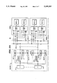
FIGS. 2A and 2B together form a block diagram of a cache coherent system according to the invention with a multiple interconnect system of multiple parallel buses interconnects multiple processors and their respective caches.
FIG. 3 is a block diagram of a monitor that is shown in FIG. 2.
FIGS. 4, 4A, 4B, and 4C when joined together form a block diagram of a cache coherent system according to the invention with a multiple interconnect system having two parallel buses interconnecting 2N multiple processors and their 2N respective caches.
FIG. 1 is a generalized block diagram of a multiple processor system 10 which includes a generalized interconnect 12 for information and control data bits. Each of the processors P1-P4 is connected to the interconnect 12 via a respective processor bus PB1-PB4. Each processor P1-P4 is also connected via its respective processor bus PB1-PB4 to a respective cache memory C1-C4 which is associated therewith. The cache memories C1-C4 reduce the access time to addresses that are frequently used by their respective processors P1-P4 because an access to a cache is faster than a similar access from main memory segments 20.
If the interconnect 12 consists of a single path between the processors P1-P4 and memory segments 20, then the caches C1-C4 are connected via the processor buses PB1-PB4 and the interconnect 12. Connected in this manner, the caches C1-C4 can monitor all of the memory accesses directly. This assumes a typical cache operation where a processor P1-P4 initiates an access by transmitting a READ or WRITE command onto its processor bus PB1-PB4 which then propagates to the memory segments 20 and the cache memories C1-C4 other than the cache associated with the accessing processor, where the associated cache will essentially interrupt the READ or WRITE from the memory segments 20 and process the READ or WRITE itself whenever the associated cache has data corresponding to the accessed address encached therein.
A problem arises, however, if the interconnect 12 consists of multiple independent paths with some of the processors P1-P4 and their respective caches being connected to one of the paths by their processor buses PB1-PB4, and the remainder of the processors P1-P4 and their caches are connected to the remaining paths. In such an arrangement, an access to the segmented memory 20 as it propagated along its path could not be directly monitored by all of the processors and their respective caches as in the single path case. Thus, in the arrangement shown in FIG. 1 if the interconnect 12 has multiple independent paths, one processor may access and change data via its path, but a cache which is connected to a different one of the multiple paths may not be able to monitor the access, even though the access renders its encached data non-coherent.
Referring now to FIGS. 2A and 2B, one embodiment of a multiple processor system 30 which prevents such data coherency problems is shown. The multiple processor system 30 includes multiple parallel buses Bus-- 1 through Bus-- K as its interconnect network. The multiple parallel buses Bus-- 1-Bus-- K provide K independent paths that connect multiple processors P11-PNP to memory segments Mem-- 1-Mem-- J. The multiple processors P11-PNP are arranged on N boards Boards-- 1-Boards-- N with P processors to a board for a total of N×P processors. Each of the multiple processors P11-PNP is connected via a respective processor bus PB11-PBNP, one per processor, to one of the multiple independent buses Bus-- 1-Bus-- K. To the extent possible, the N×P processors and their respective N×P processor buses are connected in an equally distributed fashion to the K independent paths Bus-- 1-Bus-- K in order to evenly distribute the data processing operations.
The system 30 has a cache memory architecture according to one embodiment of the invention. Each processor P11-PNP of the system 30 has a respective cache memory C11-CNP associated therewith which is connected to its respective processor bus PB11-PBNP. Each of the cache memories C11-CNP in the system 30 provides high speed local storage for a limited amount of frequently used control and data information. This local storage is used in addition to the lower speed, higher capacity main segmented memory Mem-- 1-Mem-- J. The segmented memory Mem-- 1-Mem-- J is organized in J blocks Mem-- 1-Mem-- J. Each of the blocks Mem-- 1-Mem-- J is divided into segment A and segment B. Those skilled in the art will recognize that with a minor modification each block Mem-- 1-Mem-- J may be divided into more or fewer segments, and such modifications are deemed to be within the scope of the present invention. Segment A and segment B of each block are connected through respective K-way arbitrators to the independent paths Bus-- 1-Bus-- K. With the arrangement shown in FIGS. 2A and 2B, any of the processors P11-PNP may access any address of main memory Mem-- 1-Mem-- J, and the segmentation permits concurrent accesses to addresses in different segments in order to speed up the memory system. The main memory Mem.sub. -- 1-Mem-- J is a global memory and could be used as a commonly accessible location for cache tag information of the individual caches in order to provide cache coherency, but as mentioned previously, such an approach requires a more complex main memory structure and tends to overload the paths Bus-- 1-Bus-- J with cache coherency data transfers, thereby preventing the multiple processors from being used to their greatest efficiency.
In order to provide coherency among the cache memories C11-CNP for the multiple independent path system 30 without the addition of a complex main memory sub-system or an expensive, non-standard cache bus sub-system, each of the caches C11-CNP is provided with a plurality of monitors M111-MNPK. Cache C11 is associated with a set of K monitors M111-M11K, cache C12 is associated with another set of K monitors M121-M12K, and so forth for the remaining caches and monitors. Each monitor within its set of K monitors is connected to and associated with a respective path of the K independent paths Bus-- 1-Bus-- K. These connections are actually made to the independent paths Bus-- 1-Bus-- K via the processor buses PB11-PBNP as shown in FIGS. 2A and 2B. Further, each monitor of a set is connected to the processor bus of the cache it is associated with in order to receive information about data stored therein as explained below.
Connected in this manner, each cache C11-CNP may monitor the memory accesses made on all of the independent paths Bus-- 1-Bus-- K of the multiple processor system 30. For example, processor P11 is connected via its processor bus PB11 to independent path Bus-- 1 and also to its cache C11. The cache C11 has a set of monitors M111-M11K that it is associated with. Each of the set of monitors M111-M11K is connected at one port thereof to the cache C11 via the processor bus PB11. Each of the set of monitors M111-M11K is connected at a second port thereof to one of the processor buses PB11-PB1P on Board-- 1 respectively. By the connections to PB11-PB1P, the second ports of monitors M111-M11K are also connected to Bus-- 1-Bus-- K respectively. By their first ports, the monitors M111-M11K may receive information regarding the current contents stored in its associated cache C11, e.g. cache tag information. By their second ports, the monitors M111-M11K may monitor the accesses made by all of the processors P11-PNP over the paths Bus-- 1-Bus-- K to memory Mem-- 1-Mem-- J. Thus, the monitors M111-M11K may each compare the accesses made on their respective paths Bus-- 1-Bus-- K to the addresses of information stored in their cache C11 and if any processor other than P11 is accessing and updating a corresponding address in another cache C12-CNP or in main memory Mem-- 1-Mem-- J, then C11 is informed by the monitor connected to the accessing processor's bus that its encached data is now non-coherent with the current version located in another cache or in main memory. C11, upon being informed of the non-coherency of some of its data takes appropriate action, e.g. marking the data invalid, or a flushing of the noncoherent addresses followed by a copying in of coherent data for the addresses.
Referring now to FIG. 3, the monitors M111-MNPK will be described in detail. Each of the monitors M111-MNPK has a dual port RAM 40. The dual port RAM 40 has two input/output ports PORT1, PORT2. PORT1 of each RAM 40 is connected to the processor bus PB11-PBNP of its respective cache C11-CNP and processor P11-PNP (shown in FIGS. 2A and 2B). For example, the set of monitors M111-M11K would all have PORT1 of their RAMs 40 connected to processor bus PB11 of processor P11 and cache C11. Each PORT2 of each RAM 40 of a set of monitors is connected uniquely (within its set) to one of the K independent paths Bus-- 1-Bus-- K (shown in FIGS. 2A and 2B) via one of the processor buses on its board Board-- 1-Board-- N. Thus, the set of K monitors M111-M11K would have the PORT2s of their RAMs 40 respectively connected to PB11-PB1K as their unique processor bus connections. The other sets of monitors M121-MNPK are analogously connected for their processors P12-PNP and caches C12-CNP.
The monitors M111-MNPK each have a comparator 44 connected at one input thereof to a data output portion of the PORT2 of RAM 40. A second input of each comparator 44 is connected to a group of tag bits from the most significant bits from the processor bus PB11-PBNP that the PORT2 is connected to.
In operation, dual port RAM 40 and comparator 44 are operated as a cache-tag circuit. For monitor M111, for example, when its processor P11 does a READ or a WRITE access with its cache C11 or main memory Mem-- 1-Mem-- J, the processor P11 will also sends control signals to cache C11 to indicate the cache state of the current address, e.g. valid, invalid, shared, dirty, etc. depending on the protocol of the multiple processor system. The monitor M111 will be updated at the same access from P11 and it will use the same control signals to mark the cache tags stored therein so that the monitor M111 indicates the same cache state for the cache tags of cache C11 as the encached data stored in cache C11 has. If another processor P21-PN1 connected to path Bus-- 1 does an access, monitor M111 receives the address information on PORT2 of its RAM 40 which accesses the stored cache tag information of its cache C11. The address on PORT2 will retrieve a group of tag bits from the RAM 40 and these tag bits will be compared to the tag portion of the address on PORT2. If the comparator indicates a MATCH, this means that the access of another processor on Bus-- 1 has affected the coherency of part of the data encached in C11. The MATCH signal is used as a control signal to initiate action to prevent use of this non-coherent data, i.e. mark it as invalid and/or initiate a copy from a memory having a coherent copy of the data. Those skilled in the art will understand such cache operations.
In addition to the cache coherency enforcement described above, monitors M112-M11K are connected to processor P11 and cache C11 at the PORT1s of their RAMs 40, just as M111 is. Further, monitors M112-M11K are updated by processor P11 as to the addresses and state of the data encached in cache C11, just as monitor M111 is updated. But, instead of monitoring the same path Bus-- 1 for accesses affecting the state of the data encached in C11, M112-M11K monitor paths Bus-- 2-Bus-- K respectively. Thus, if a processor connected to paths Bus-- 2-Bus-- K accesses an address that corresponds to an address of data encached in C11, and that access affects the coherency of the data in cache C11 for that address, then the monitor, from the set of monitors M111-M11K, that is uniquely attached to the path over which the access is made will receive the address on PORT2 of its RAM 40. This access address on its PORT2 will retrieve a group of index bits from the RAM 40 and these index bits will be compared to the index portion of the address on PORT2. If the comparator indicates a MATCH, this means that the access of another processor on another path Bus-- 2-Bus-- K has affected the coherency of part of the data encached in C11. This MATCH signal is then used to initiate action to prevent use of this non-coherent data, i.e. mark it as invalid and/or initiate a copy from a memory having a coherent copy of the data, in a similar manner to a MATCH generated by an access on path Bus-- 1 described previously.
FIGS. 4A, 4B, and 4C together shows a specific embodiment of the invention described above in connection with FIGS. 2A and 2B in which K is two. This embodiment of the invention is of particular interest because systems with two parallel buses have been built, and standard hardware, i.e. the back plane and board cabinet, are readily available. For a two parallel bus system, such as the system 50 shown in FIGS. 4A, 4B, and 4C, cache monitors and their interconnections could be added at the board level, and standard back plane and cabinet level hardware of a two parallel bus system, such as a Future Bus system, could be used.
Thus, it will now be understood that there has been disclosed a cache coherency method and apparatus for a multiple path interconnection system which provides cache coherency for all caches without the addition of a cache-to-cache bus subsystem. While the invention has been particularly illustrated and described with reference to a preferred embodiment thereof, it will be understood by those skilled in the art that various changes in form, details, and applications may be made therein. It is accordingly intended that the appended claims shall cover all such changes in form, details and applications which do not depart from the true spirit and scope of the invention.
Claims (16)
Priority Applications (1)
Application Number | Priority Date | Filing Date | Title |
---|---|---|---|
US07633732 US5249283A (en) | 1990-12-24 | 1990-12-24 | Cache coherency method and apparatus for a multiple path interconnection network |
Applications Claiming Priority (1)
Application Number | Priority Date | Filing Date | Title |
---|---|---|---|
US07633732 US5249283A (en) | 1990-12-24 | 1990-12-24 | Cache coherency method and apparatus for a multiple path interconnection network |
Publications (1)
Publication Number | Publication Date |
---|---|
US5249283A true US5249283A (en) | 1993-09-28 |
Family
ID=24540891
Family Applications (1)
Application Number | Title | Priority Date | Filing Date |
---|---|---|---|
US07633732 Expired - Fee Related US5249283A (en) | 1990-12-24 | 1990-12-24 | Cache coherency method and apparatus for a multiple path interconnection network |
Country Status (1)
Country | Link |
---|---|
US (1) | US5249283A (en) |
Cited By (27)
Publication number | Priority date | Publication date | Assignee | Title |
---|---|---|---|---|
US5442758A (en) * | 1993-07-19 | 1995-08-15 | Sequent Computer Systems, Inc. | Apparatus and method for achieving reduced overhead mutual exclusion and maintaining coherency in a multiprocessor system utilizing execution history and thread monitoring |
US5469555A (en) * | 1991-12-19 | 1995-11-21 | Opti, Inc. | Adaptive write-back method and apparatus wherein the cache system operates in a combination of write-back and write-through modes for a cache-based microprocessor system |
US5513335A (en) * | 1992-11-02 | 1996-04-30 | Sgs-Thomson Microelectronics, Inc. | Cache tag memory having first and second single-port arrays and a dual-port array |
US5551048A (en) * | 1994-06-03 | 1996-08-27 | Digital Equipment Corporation | Ring based distributed communication bus for a multiprocessor network |
EP0751466A2 (en) * | 1995-06-30 | 1997-01-02 | Siemens Nixdorf Informationssysteme AG | Multiprocessor system with a very large number of microprocessors |
US5630095A (en) * | 1993-08-03 | 1997-05-13 | Motorola Inc. | Method for use with a data coherency protocol allowing multiple snoop queries to a single snoop transaction and system therefor |
US5634027A (en) * | 1991-11-20 | 1997-05-27 | Kabushiki Kaisha Toshiba | Cache memory system for multiple processors with collectively arranged cache tag memories |
US5636361A (en) * | 1994-12-22 | 1997-06-03 | International Business Machines Corporation | Multi-processor computer system having dual memory subsytems for enabling concurrent memory access thereto by more than one processor |
US5659784A (en) * | 1994-01-28 | 1997-08-19 | Nec Corporation | Multi-processor system having communication register modules using test-and-set request operation for synchronizing communications |
US5659710A (en) * | 1995-11-29 | 1997-08-19 | International Business Machines Corporation | Cache coherency method and system employing serially encoded snoop responses |
US5680575A (en) * | 1992-02-20 | 1997-10-21 | International Business Machines Corporation | Interconnect failure detection and cache reset apparatus |
US5778437A (en) * | 1995-09-25 | 1998-07-07 | International Business Machines Corporation | Invalidation bus optimization for multiprocessors using directory-based cache coherence protocols in which an address of a line to be modified is placed on the invalidation bus simultaneously with sending a modify request to the directory |
US5809537A (en) * | 1995-12-08 | 1998-09-15 | International Business Machines Corp. | Method and system for simultaneous processing of snoop and cache operations |
US5829037A (en) * | 1992-08-19 | 1998-10-27 | Siemens Nixdorf Informationssysteme Aktiengesellschaft | Multiprocessor system having a large number of processor system components connected to a plurality of serial high-speed-buses |
US5893149A (en) * | 1996-07-01 | 1999-04-06 | Sun Microsystems, Inc. | Flushing of cache memory in a computer system |
US5991819A (en) * | 1996-12-03 | 1999-11-23 | Intel Corporation | Dual-ported memory controller which maintains cache coherency using a memory line status table |
US6658520B1 (en) * | 2000-09-26 | 2003-12-02 | Intel Corporation | Method and system for keeping two independent busses coherent following a direct memory access |
US6697076B1 (en) * | 2001-12-31 | 2004-02-24 | Apple Computer, Inc. | Method and apparatus for address re-mapping |
US20040143626A1 (en) * | 2003-01-21 | 2004-07-22 | Dell Products L.P. | Method and system for operating a cache for multiple files |
US20060036809A1 (en) * | 2004-06-30 | 2006-02-16 | Kevin Rudd | Methods and apparatus for enforcing instruction-cache coherence |
US7015921B1 (en) * | 2001-12-31 | 2006-03-21 | Apple Computer, Inc. | Method and apparatus for memory access |
US7034849B1 (en) | 2001-12-31 | 2006-04-25 | Apple Computer, Inc. | Method and apparatus for image blending |
US7681013B1 (en) | 2001-12-31 | 2010-03-16 | Apple Inc. | Method for variable length decoding using multiple configurable look-up tables |
US20110161596A1 (en) * | 2009-12-28 | 2011-06-30 | Conte Tom | Directory-based coherence caching |
US20120144064A1 (en) * | 2010-11-05 | 2012-06-07 | Cray Inc. | Progressive adaptive routing in a dragonfly processor interconnect network |
US9282037B2 (en) | 2010-11-05 | 2016-03-08 | Intel Corporation | Table-driven routing in a dragonfly processor interconnect network |
US9614786B2 (en) | 2008-08-20 | 2017-04-04 | Intel Corporation | Dragonfly processor interconnect network |
Citations (25)
Publication number | Priority date | Publication date | Assignee | Title |
---|---|---|---|---|
US4136386A (en) * | 1977-10-06 | 1979-01-23 | International Business Machines Corporation | Backing store access coordination in a multi-processor system |
US4141067A (en) * | 1977-06-13 | 1979-02-20 | General Automation | Multiprocessor system with cache memory |
US4392200A (en) * | 1980-01-28 | 1983-07-05 | Digital Equipment Corporation | Cached multiprocessor system with pipeline timing |
US4467454A (en) * | 1980-12-29 | 1984-08-21 | Fujitsu Limited | High-speed external memory system |
US4493030A (en) * | 1981-05-29 | 1985-01-08 | The General Electric Company P.L.C. | Plural data processor groups controlling a telecommunications exchange |
US4541076A (en) * | 1982-05-13 | 1985-09-10 | Storage Technology Corporation | Dual port CMOS random access memory |
US4577293A (en) * | 1984-06-01 | 1986-03-18 | International Business Machines Corporation | Distributed, on-chip cache |
US4622631A (en) * | 1983-12-30 | 1986-11-11 | Plexus Computers, Inc. | Data processing system having a data coherence solution |
US4669043A (en) * | 1984-02-17 | 1987-05-26 | Signetics Corporation | Memory access controller |
US4695943A (en) * | 1984-09-27 | 1987-09-22 | Honeywell Information Systems Inc. | Multiprocessor shared pipeline cache memory with split cycle and concurrent utilization |
US4754398A (en) * | 1985-06-28 | 1988-06-28 | Cray Research, Inc. | System for multiprocessor communication using local and common semaphore and information registers |
US4783736A (en) * | 1985-07-22 | 1988-11-08 | Alliant Computer Systems Corporation | Digital computer with multisection cache |
US4825360A (en) * | 1986-07-30 | 1989-04-25 | Symbolics, Inc. | System and method for parallel processing with mostly functional languages |
US4833601A (en) * | 1987-05-28 | 1989-05-23 | Bull Hn Information Systems Inc. | Cache resiliency in processing a variety of address faults |
US4933909A (en) * | 1988-12-19 | 1990-06-12 | Bull Hn Information Systems Inc. | Dual read/write register file memory |
US4939641A (en) * | 1988-06-30 | 1990-07-03 | Wang Laboratories, Inc. | Multi-processor system with cache memories |
US4975872A (en) * | 1988-11-17 | 1990-12-04 | Matsushita Electric Industrial Co., Ltd. | Dual port memory device with tag bit marking |
US5008813A (en) * | 1987-12-05 | 1991-04-16 | International Computers Limited | Multi-cache data storage system |
US5014247A (en) * | 1988-12-19 | 1991-05-07 | Advanced Micro Devices, Inc. | System for accessing the same memory location by two different devices |
US5025365A (en) * | 1988-11-14 | 1991-06-18 | Unisys Corporation | Hardware implemented cache coherency protocol with duplicated distributed directories for high-performance multiprocessors |
US5058006A (en) * | 1988-06-27 | 1991-10-15 | Digital Equipment Corporation | Method and apparatus for filtering invalidate requests |
US5060144A (en) * | 1989-03-16 | 1991-10-22 | Unisys Corporation | Locking control with validity status indication for a multi-host processor system that utilizes a record lock processor and a cache memory for each host processor |
US5072369A (en) * | 1989-04-07 | 1991-12-10 | Tektronix, Inc. | Interface between buses attached with cached modules providing address space mapped cache coherent memory access with SNOOP hit memory updates |
US5091846A (en) * | 1986-10-03 | 1992-02-25 | Intergraph Corporation | Cache providing caching/non-caching write-through and copyback modes for virtual addresses and including bus snooping to maintain coherency |
US5097409A (en) * | 1988-06-30 | 1992-03-17 | Wang Laboratories, Inc. | Multi-processor system with cache memories |
Patent Citations (26)
Publication number | Priority date | Publication date | Assignee | Title |
---|---|---|---|---|
US4141067A (en) * | 1977-06-13 | 1979-02-20 | General Automation | Multiprocessor system with cache memory |
US4136386A (en) * | 1977-10-06 | 1979-01-23 | International Business Machines Corporation | Backing store access coordination in a multi-processor system |
US4392200A (en) * | 1980-01-28 | 1983-07-05 | Digital Equipment Corporation | Cached multiprocessor system with pipeline timing |
US4467454A (en) * | 1980-12-29 | 1984-08-21 | Fujitsu Limited | High-speed external memory system |
US4493030A (en) * | 1981-05-29 | 1985-01-08 | The General Electric Company P.L.C. | Plural data processor groups controlling a telecommunications exchange |
US4541076A (en) * | 1982-05-13 | 1985-09-10 | Storage Technology Corporation | Dual port CMOS random access memory |
US4622631A (en) * | 1983-12-30 | 1986-11-11 | Plexus Computers, Inc. | Data processing system having a data coherence solution |
US4622631B1 (en) * | 1983-12-30 | 1996-04-09 | Recognition Int Inc | Data processing system having a data coherence solution |
US4669043A (en) * | 1984-02-17 | 1987-05-26 | Signetics Corporation | Memory access controller |
US4577293A (en) * | 1984-06-01 | 1986-03-18 | International Business Machines Corporation | Distributed, on-chip cache |
US4695943A (en) * | 1984-09-27 | 1987-09-22 | Honeywell Information Systems Inc. | Multiprocessor shared pipeline cache memory with split cycle and concurrent utilization |
US4754398A (en) * | 1985-06-28 | 1988-06-28 | Cray Research, Inc. | System for multiprocessor communication using local and common semaphore and information registers |
US4783736A (en) * | 1985-07-22 | 1988-11-08 | Alliant Computer Systems Corporation | Digital computer with multisection cache |
US4825360A (en) * | 1986-07-30 | 1989-04-25 | Symbolics, Inc. | System and method for parallel processing with mostly functional languages |
US5091846A (en) * | 1986-10-03 | 1992-02-25 | Intergraph Corporation | Cache providing caching/non-caching write-through and copyback modes for virtual addresses and including bus snooping to maintain coherency |
US4833601A (en) * | 1987-05-28 | 1989-05-23 | Bull Hn Information Systems Inc. | Cache resiliency in processing a variety of address faults |
US5008813A (en) * | 1987-12-05 | 1991-04-16 | International Computers Limited | Multi-cache data storage system |
US5058006A (en) * | 1988-06-27 | 1991-10-15 | Digital Equipment Corporation | Method and apparatus for filtering invalidate requests |
US4939641A (en) * | 1988-06-30 | 1990-07-03 | Wang Laboratories, Inc. | Multi-processor system with cache memories |
US5097409A (en) * | 1988-06-30 | 1992-03-17 | Wang Laboratories, Inc. | Multi-processor system with cache memories |
US5025365A (en) * | 1988-11-14 | 1991-06-18 | Unisys Corporation | Hardware implemented cache coherency protocol with duplicated distributed directories for high-performance multiprocessors |
US4975872A (en) * | 1988-11-17 | 1990-12-04 | Matsushita Electric Industrial Co., Ltd. | Dual port memory device with tag bit marking |
US4933909A (en) * | 1988-12-19 | 1990-06-12 | Bull Hn Information Systems Inc. | Dual read/write register file memory |
US5014247A (en) * | 1988-12-19 | 1991-05-07 | Advanced Micro Devices, Inc. | System for accessing the same memory location by two different devices |
US5060144A (en) * | 1989-03-16 | 1991-10-22 | Unisys Corporation | Locking control with validity status indication for a multi-host processor system that utilizes a record lock processor and a cache memory for each host processor |
US5072369A (en) * | 1989-04-07 | 1991-12-10 | Tektronix, Inc. | Interface between buses attached with cached modules providing address space mapped cache coherent memory access with SNOOP hit memory updates |
Non-Patent Citations (12)
Title |
---|
"A Class of Compatible Cache Consistency Protocols and Their Support by the IEEE Futurebus" by Paul Sweazey and Alan Jay Smith, IEEE Paper, 1986, pp. 414-423. |
"Analysis of Multiprocessors with Private Cache Memories," by Janak H. Patel, IEEE Transactions on Computers, vol. C-31, No. 4, Apr. 1982, pp. 296-304. |
"Effects of Cache Coherency in Multiprocessors," by Michel DuBois, IEEE Transactions on Computers, vol. C-31, No. 11, Nov. 1982, pp. 1083-1099. |
"Parallel Processing with the Perfect Shuffle," by Harold S. Stone, IEEE Transactions on Computers, vol. C-20, No. 2, Feb. 1971, pp. 153-161. |
"Performance of Processor-Memory Interconnections for Multiprocessors," by Janak H. Patel, IEEE Transactions on Computers, vol. C-30, No. 10, Oct. 1981, pp. 771-780. |
"The Wisconsin Multicube: A New Large-Scale Cache-Coherent Multiprocessor," by James R. Goodman and Philip J. Woest, 1988 International Symposium on Computer Architecture. |
A Class of Compatible Cache Consistency Protocols and Their Support by the IEEE Futurebus by Paul Sweazey and Alan Jay Smith, IEEE Paper, 1986, pp. 414 423. * |
Analysis of Multiprocessors with Private Cache Memories, by Janak H. Patel, IEEE Transactions on Computers, vol. C 31, No. 4, Apr. 1982, pp. 296 304. * |
Effects of Cache Coherency in Multiprocessors, by Michel DuBois, IEEE Transactions on Computers, vol. C 31, No. 11, Nov. 1982, pp. 1083 1099. * |
Parallel Processing with the Perfect Shuffle, by Harold S. Stone, IEEE Transactions on Computers, vol. C 20, No. 2, Feb. 1971, pp. 153 161. * |
Performance of Processor Memory Interconnections for Multiprocessors, by Janak H. Patel, IEEE Transactions on Computers, vol. C 30, No. 10, Oct. 1981, pp. 771 780. * |
The Wisconsin Multicube: A New Large Scale Cache Coherent Multiprocessor, by James R. Goodman and Philip J. Woest, 1988 International Symposium on Computer Architecture. * |
Cited By (39)
Publication number | Priority date | Publication date | Assignee | Title |
---|---|---|---|---|
US5634027A (en) * | 1991-11-20 | 1997-05-27 | Kabushiki Kaisha Toshiba | Cache memory system for multiple processors with collectively arranged cache tag memories |
US5469555A (en) * | 1991-12-19 | 1995-11-21 | Opti, Inc. | Adaptive write-back method and apparatus wherein the cache system operates in a combination of write-back and write-through modes for a cache-based microprocessor system |
US5680575A (en) * | 1992-02-20 | 1997-10-21 | International Business Machines Corporation | Interconnect failure detection and cache reset apparatus |
US5829037A (en) * | 1992-08-19 | 1998-10-27 | Siemens Nixdorf Informationssysteme Aktiengesellschaft | Multiprocessor system having a large number of processor system components connected to a plurality of serial high-speed-buses |
US5513335A (en) * | 1992-11-02 | 1996-04-30 | Sgs-Thomson Microelectronics, Inc. | Cache tag memory having first and second single-port arrays and a dual-port array |
US6219690B1 (en) | 1993-07-19 | 2001-04-17 | International Business Machines Corporation | Apparatus and method for achieving reduced overhead mutual exclusion and maintaining coherency in a multiprocessor system utilizing execution history and thread monitoring |
US5608893A (en) * | 1993-07-19 | 1997-03-04 | Sequent Computer Systems, Inc. | Method for maintaining data coherency using thread activity summaries in a multicomputer system |
US5727209A (en) * | 1993-07-19 | 1998-03-10 | Sequent Computer Systems, Inc. | Apparatus and method for achieving reduced overhead mutual-exclusion and maintaining coherency in a multiprocessor system utilizing execution history and thread monitoring |
US5442758A (en) * | 1993-07-19 | 1995-08-15 | Sequent Computer Systems, Inc. | Apparatus and method for achieving reduced overhead mutual exclusion and maintaining coherency in a multiprocessor system utilizing execution history and thread monitoring |
US5630095A (en) * | 1993-08-03 | 1997-05-13 | Motorola Inc. | Method for use with a data coherency protocol allowing multiple snoop queries to a single snoop transaction and system therefor |
US5659784A (en) * | 1994-01-28 | 1997-08-19 | Nec Corporation | Multi-processor system having communication register modules using test-and-set request operation for synchronizing communications |
US5551048A (en) * | 1994-06-03 | 1996-08-27 | Digital Equipment Corporation | Ring based distributed communication bus for a multiprocessor network |
US5636361A (en) * | 1994-12-22 | 1997-06-03 | International Business Machines Corporation | Multi-processor computer system having dual memory subsytems for enabling concurrent memory access thereto by more than one processor |
EP0751466A3 (en) * | 1995-06-30 | 1998-03-18 | Siemens Nixdorf Informationssysteme AG | Multiprocessor system with a very large number of microprocessors |
EP0751466A2 (en) * | 1995-06-30 | 1997-01-02 | Siemens Nixdorf Informationssysteme AG | Multiprocessor system with a very large number of microprocessors |
DE19524023B4 (en) * | 1995-06-30 | 2004-02-05 | Fujitsu Siemens Computers Gmbh | Multiprocessor system with a very large number of microprocessors |
US5778437A (en) * | 1995-09-25 | 1998-07-07 | International Business Machines Corporation | Invalidation bus optimization for multiprocessors using directory-based cache coherence protocols in which an address of a line to be modified is placed on the invalidation bus simultaneously with sending a modify request to the directory |
US5659710A (en) * | 1995-11-29 | 1997-08-19 | International Business Machines Corporation | Cache coherency method and system employing serially encoded snoop responses |
US5809537A (en) * | 1995-12-08 | 1998-09-15 | International Business Machines Corp. | Method and system for simultaneous processing of snoop and cache operations |
US5893149A (en) * | 1996-07-01 | 1999-04-06 | Sun Microsystems, Inc. | Flushing of cache memory in a computer system |
US5991819A (en) * | 1996-12-03 | 1999-11-23 | Intel Corporation | Dual-ported memory controller which maintains cache coherency using a memory line status table |
US6658520B1 (en) * | 2000-09-26 | 2003-12-02 | Intel Corporation | Method and system for keeping two independent busses coherent following a direct memory access |
US7681013B1 (en) | 2001-12-31 | 2010-03-16 | Apple Inc. | Method for variable length decoding using multiple configurable look-up tables |
US20070242085A1 (en) * | 2001-12-31 | 2007-10-18 | Weybrew Steven T | Method and apparatus for image blending |
US6697076B1 (en) * | 2001-12-31 | 2004-02-24 | Apple Computer, Inc. | Method and apparatus for address re-mapping |
US7015921B1 (en) * | 2001-12-31 | 2006-03-21 | Apple Computer, Inc. | Method and apparatus for memory access |
US7034849B1 (en) | 2001-12-31 | 2006-04-25 | Apple Computer, Inc. | Method and apparatus for image blending |
US20060114264A1 (en) * | 2001-12-31 | 2006-06-01 | Weybrew Steven T | Method and apparatus for image blending |
US7230633B2 (en) | 2001-12-31 | 2007-06-12 | Apple Inc. | Method and apparatus for image blending |
US7548248B2 (en) | 2001-12-31 | 2009-06-16 | Apple Inc. | Method and apparatus for image blending |
US20040143626A1 (en) * | 2003-01-21 | 2004-07-22 | Dell Products L.P. | Method and system for operating a cache for multiple files |
US7426612B2 (en) * | 2004-06-30 | 2008-09-16 | Intel Corporation | Methods and apparatus for enforcing instruction-cache coherence |
US20060036809A1 (en) * | 2004-06-30 | 2006-02-16 | Kevin Rudd | Methods and apparatus for enforcing instruction-cache coherence |
US9614786B2 (en) | 2008-08-20 | 2017-04-04 | Intel Corporation | Dragonfly processor interconnect network |
US20110161596A1 (en) * | 2009-12-28 | 2011-06-30 | Conte Tom | Directory-based coherence caching |
US8874855B2 (en) * | 2009-12-28 | 2014-10-28 | Empire Technology Development Llc | Directory-based coherence caching |
US20120144064A1 (en) * | 2010-11-05 | 2012-06-07 | Cray Inc. | Progressive adaptive routing in a dragonfly processor interconnect network |
US9137143B2 (en) * | 2010-11-05 | 2015-09-15 | Intel Corporation | Progressive adaptive routing in a dragonfly processor interconnect network |
US9282037B2 (en) | 2010-11-05 | 2016-03-08 | Intel Corporation | Table-driven routing in a dragonfly processor interconnect network |
Similar Documents
Publication | Publication Date | Title |
---|---|---|
US5148533A (en) | Apparatus and method for data group coherency in a tightly coupled data processing system with plural execution and data cache units | |
US6591321B1 (en) | Multiprocessor system bus protocol with group addresses, responses, and priorities | |
US5561779A (en) | Processor board having a second level writeback cache system and a third level writethrough cache system which stores exclusive state information for use in a multiprocessor computer system | |
Katz et al. | Implementing a cache consistency protocol | |
US6014756A (en) | High availability error self-recovering shared cache for multiprocessor systems | |
US6799252B1 (en) | High-performance modular memory system with crossbar connections | |
US5226150A (en) | Apparatus for suppressing an error report from an address for which an error has already been reported | |
US6122711A (en) | Method of and apparatus for store-in second level cache flush | |
US5490253A (en) | Multiprocessor system using odd/even data buses with a timeshared address bus | |
US5067078A (en) | Cache which provides status information | |
US4733352A (en) | Lock control for a shared storage in a data processing system | |
US6088769A (en) | Multiprocessor cache coherence directed by combined local and global tables | |
US6243794B1 (en) | Data-processing system with CC-NUMA (cache-coherent, non-uniform memory access) architecture and remote cache incorporated in local memory | |
US6487643B1 (en) | Method and apparatus for preventing starvation in a multi-node architecture | |
US4977498A (en) | Data processing system having a data memory interlock coherency scheme | |
US6516372B1 (en) | Partitioning a distributed shared memory multiprocessor computer to facilitate selective hardware maintenance | |
US5265232A (en) | Coherence control by data invalidation in selected processor caches without broadcasting to processor caches not having the data | |
US4458310A (en) | Cache memory using a lowest priority replacement circuit | |
US4747070A (en) | Reconfigurable memory system | |
US6615319B2 (en) | Distributed mechanism for resolving cache coherence conflicts in a multi-node computer architecture | |
US6151663A (en) | Cluster controller for memory and data cache in a multiple cluster processing system | |
US6536000B1 (en) | Communication error reporting mechanism in a multiprocessing computer system | |
US5987571A (en) | Cache coherency control method and multi-processor system using the same | |
US5696937A (en) | Cache controller utilizing a state machine for controlling invalidations in a network with dual system busses | |
US20050240736A1 (en) | System and method for coherency filtering |
Legal Events
Date | Code | Title | Description |
---|---|---|---|
AS | Assignment |
Owner name: NCR CORPORATION, DAYTON, OHIO A CORP. OF MD Free format text: ASSIGNMENT OF ASSIGNORS INTEREST.;ASSIGNOR:BOLAND, VERNON K.;REEL/FRAME:005560/0019 Effective date: 19901219 |
|
CC | Certificate of correction | ||
FPAY | Fee payment |
Year of fee payment: 4 |
|
FPAY | Fee payment |
Year of fee payment: 8 |
|
REMI | Maintenance fee reminder mailed | ||
LAPS | Lapse for failure to pay maintenance fees | ||
FP | Expired due to failure to pay maintenance fee |
Effective date: 20050928 |