US5213937A - Process for preparing an electrophotographic photoreceptor - Google Patents
Process for preparing an electrophotographic photoreceptor Download PDFInfo
- Publication number
- US5213937A US5213937A US07/791,563 US79156391A US5213937A US 5213937 A US5213937 A US 5213937A US 79156391 A US79156391 A US 79156391A US 5213937 A US5213937 A US 5213937A
- Authority
- US
- United States
- Prior art keywords
- layer
- temperature
- coating solution
- carrier generation
- coating
- Prior art date
- Legal status (The legal status is an assumption and is not a legal conclusion. Google has not performed a legal analysis and makes no representation as to the accuracy of the status listed.)
- Expired - Lifetime
Links
- 108091008695 photoreceptors Proteins 0.000 title claims abstract description 33
- 238000004519 manufacturing process Methods 0.000 title description 4
- 238000000576 coating method Methods 0.000 claims abstract description 94
- 239000011248 coating agent Substances 0.000 claims abstract description 89
- 238000000034 method Methods 0.000 claims abstract description 16
- 229910052782 aluminium Inorganic materials 0.000 claims abstract description 8
- XAGFODPZIPBFFR-UHFFFAOYSA-N aluminium Chemical compound [Al] XAGFODPZIPBFFR-UHFFFAOYSA-N 0.000 claims abstract description 8
- 238000001035 drying Methods 0.000 claims description 10
- 238000007598 dipping method Methods 0.000 claims description 7
- 239000000463 material Substances 0.000 abstract 1
- 239000010410 layer Substances 0.000 description 107
- 238000012360 testing method Methods 0.000 description 23
- 229920005989 resin Polymers 0.000 description 13
- 239000011347 resin Substances 0.000 description 13
- 238000002360 preparation method Methods 0.000 description 9
- LFQSCWFLJHTTHZ-UHFFFAOYSA-N Ethanol Chemical group CCO LFQSCWFLJHTTHZ-UHFFFAOYSA-N 0.000 description 8
- CSCPPACGZOOCGX-UHFFFAOYSA-N Acetone Chemical compound CC(C)=O CSCPPACGZOOCGX-UHFFFAOYSA-N 0.000 description 7
- 239000002904 solvent Substances 0.000 description 7
- 238000011282 treatment Methods 0.000 description 7
- ZWEHNKRNPOVVGH-UHFFFAOYSA-N 2-Butanone Chemical compound CCC(C)=O ZWEHNKRNPOVVGH-UHFFFAOYSA-N 0.000 description 6
- OKKJLVBELUTLKV-UHFFFAOYSA-N Methanol Chemical compound OC OKKJLVBELUTLKV-UHFFFAOYSA-N 0.000 description 6
- 239000000049 pigment Substances 0.000 description 6
- 239000000126 substance Substances 0.000 description 6
- 238000010586 diagram Methods 0.000 description 5
- HEDRZPFGACZZDS-UHFFFAOYSA-N Chloroform Chemical compound ClC(Cl)Cl HEDRZPFGACZZDS-UHFFFAOYSA-N 0.000 description 4
- KFZMGEQAYNKOFK-UHFFFAOYSA-N Isopropanol Chemical compound CC(C)O KFZMGEQAYNKOFK-UHFFFAOYSA-N 0.000 description 4
- 238000003618 dip coating Methods 0.000 description 4
- 239000011241 protective layer Substances 0.000 description 4
- -1 tetrahydrofran Chemical class 0.000 description 4
- UHOVQNZJYSORNB-UHFFFAOYSA-N Benzene Chemical compound C1=CC=CC=C1 UHOVQNZJYSORNB-UHFFFAOYSA-N 0.000 description 3
- YMWUJEATGCHHMB-UHFFFAOYSA-N Dichloromethane Chemical compound ClCCl YMWUJEATGCHHMB-UHFFFAOYSA-N 0.000 description 3
- XEKOWRVHYACXOJ-UHFFFAOYSA-N Ethyl acetate Chemical compound CCOC(C)=O XEKOWRVHYACXOJ-UHFFFAOYSA-N 0.000 description 3
- ZMXDDKWLCZADIW-UHFFFAOYSA-N N,N-Dimethylformamide Chemical compound CN(C)C=O ZMXDDKWLCZADIW-UHFFFAOYSA-N 0.000 description 3
- 206010034972 Photosensitivity reaction Diseases 0.000 description 3
- YXFVVABEGXRONW-UHFFFAOYSA-N Toluene Chemical compound CC1=CC=CC=C1 YXFVVABEGXRONW-UHFFFAOYSA-N 0.000 description 3
- 239000011230 binding agent Substances 0.000 description 3
- 230000000052 comparative effect Effects 0.000 description 3
- 229910003460 diamond Inorganic materials 0.000 description 3
- 239000010432 diamond Substances 0.000 description 3
- 239000000428 dust Substances 0.000 description 3
- 230000036211 photosensitivity Effects 0.000 description 3
- XLYOFNOQVPJJNP-UHFFFAOYSA-N water Substances O XLYOFNOQVPJJNP-UHFFFAOYSA-N 0.000 description 3
- WSLDOOZREJYCGB-UHFFFAOYSA-N 1,2-Dichloroethane Chemical compound ClCCCl WSLDOOZREJYCGB-UHFFFAOYSA-N 0.000 description 2
- AZQWKYJCGOJGHM-UHFFFAOYSA-N 1,4-benzoquinone Chemical compound O=C1C=CC(=O)C=C1 AZQWKYJCGOJGHM-UHFFFAOYSA-N 0.000 description 2
- IAZDPXIOMUYVGZ-UHFFFAOYSA-N Dimethylsulphoxide Chemical compound CS(C)=O IAZDPXIOMUYVGZ-UHFFFAOYSA-N 0.000 description 2
- 239000004372 Polyvinyl alcohol Substances 0.000 description 2
- XLOMVQKBTHCTTD-UHFFFAOYSA-N Zinc monoxide Chemical compound [Zn]=O XLOMVQKBTHCTTD-UHFFFAOYSA-N 0.000 description 2
- MWPLVEDNUUSJAV-UHFFFAOYSA-N anthracene Chemical compound C1=CC=CC2=CC3=CC=CC=C3C=C21 MWPLVEDNUUSJAV-UHFFFAOYSA-N 0.000 description 2
- 230000015572 biosynthetic process Effects 0.000 description 2
- IISBACLAFKSPIT-UHFFFAOYSA-N bisphenol A Chemical compound C=1C=C(O)C=CC=1C(C)(C)C1=CC=C(O)C=C1 IISBACLAFKSPIT-UHFFFAOYSA-N 0.000 description 2
- 239000005018 casein Substances 0.000 description 2
- BECPQYXYKAMYBN-UHFFFAOYSA-N casein, tech. Chemical compound NCCCCC(C(O)=O)N=C(O)C(CC(O)=O)N=C(O)C(CCC(O)=N)N=C(O)C(CC(C)C)N=C(O)C(CCC(O)=O)N=C(O)C(CC(O)=O)N=C(O)C(CCC(O)=O)N=C(O)C(C(C)O)N=C(O)C(CCC(O)=N)N=C(O)C(CCC(O)=N)N=C(O)C(CCC(O)=N)N=C(O)C(CCC(O)=O)N=C(O)C(CCC(O)=O)N=C(O)C(COP(O)(O)=O)N=C(O)C(CCC(O)=N)N=C(O)C(N)CC1=CC=CC=C1 BECPQYXYKAMYBN-UHFFFAOYSA-N 0.000 description 2
- 235000021240 caseins Nutrition 0.000 description 2
- 229920001577 copolymer Polymers 0.000 description 2
- 239000013078 crystal Substances 0.000 description 2
- JHIVVAPYMSGYDF-UHFFFAOYSA-N cyclohexanone Chemical compound O=C1CCCCC1 JHIVVAPYMSGYDF-UHFFFAOYSA-N 0.000 description 2
- 238000007602 hot air drying Methods 0.000 description 2
- 150000002576 ketones Chemical class 0.000 description 2
- 229920002521 macromolecule Polymers 0.000 description 2
- 238000005259 measurement Methods 0.000 description 2
- 229910052751 metal Inorganic materials 0.000 description 2
- 239000002184 metal Substances 0.000 description 2
- XNGIFLGASWRNHJ-UHFFFAOYSA-N phthalic acid Chemical compound OC(=O)C1=CC=CC=C1C(O)=O XNGIFLGASWRNHJ-UHFFFAOYSA-N 0.000 description 2
- 229920003227 poly(N-vinyl carbazole) Polymers 0.000 description 2
- 239000004417 polycarbonate Substances 0.000 description 2
- 229920000515 polycarbonate Polymers 0.000 description 2
- 229920002451 polyvinyl alcohol Polymers 0.000 description 2
- 235000019422 polyvinyl alcohol Nutrition 0.000 description 2
- BBEAQIROQSPTKN-UHFFFAOYSA-N pyrene Chemical compound C1=CC=C2C=CC3=CC=CC4=CC=C1C2=C43 BBEAQIROQSPTKN-UHFFFAOYSA-N 0.000 description 2
- 230000000717 retained effect Effects 0.000 description 2
- 239000007787 solid Substances 0.000 description 2
- VZGDMQKNWNREIO-UHFFFAOYSA-N tetrachloromethane Chemical compound ClC(Cl)(Cl)Cl VZGDMQKNWNREIO-UHFFFAOYSA-N 0.000 description 2
- 229920002554 vinyl polymer Polymers 0.000 description 2
- 238000005406 washing Methods 0.000 description 2
- SJHPCNCNNSSLPL-CSKARUKUSA-N (4e)-4-(ethoxymethylidene)-2-phenyl-1,3-oxazol-5-one Chemical class O1C(=O)C(=C/OCC)\N=C1C1=CC=CC=C1 SJHPCNCNNSSLPL-CSKARUKUSA-N 0.000 description 1
- LGXVIGDEPROXKC-UHFFFAOYSA-N 1,1-dichloroethene Chemical group ClC(Cl)=C LGXVIGDEPROXKC-UHFFFAOYSA-N 0.000 description 1
- KFUSEUYYWQURPO-UHFFFAOYSA-N 1,2-dichloroethene Chemical group ClC=CCl KFUSEUYYWQURPO-UHFFFAOYSA-N 0.000 description 1
- RYHBNJHYFVUHQT-UHFFFAOYSA-N 1,4-Dioxane Chemical compound C1COCCO1 RYHBNJHYFVUHQT-UHFFFAOYSA-N 0.000 description 1
- OCJBOOLMMGQPQU-UHFFFAOYSA-N 1,4-dichlorobenzene Chemical compound ClC1=CC=C(Cl)C=C1 OCJBOOLMMGQPQU-UHFFFAOYSA-N 0.000 description 1
- WPMHMYHJGDAHKX-UHFFFAOYSA-N 1-ethenylpyrene Chemical compound C1=C2C(C=C)=CC=C(C=C3)C2=C2C3=CC=CC2=C1 WPMHMYHJGDAHKX-UHFFFAOYSA-N 0.000 description 1
- BIEFDNUEROKZRA-UHFFFAOYSA-N 2-(2-phenylethenyl)aniline Chemical class NC1=CC=CC=C1C=CC1=CC=CC=C1 BIEFDNUEROKZRA-UHFFFAOYSA-N 0.000 description 1
- XNWFRZJHXBZDAG-UHFFFAOYSA-N 2-METHOXYETHANOL Chemical compound COCCO XNWFRZJHXBZDAG-UHFFFAOYSA-N 0.000 description 1
- WUPHOULIZUERAE-UHFFFAOYSA-N 3-(oxolan-2-yl)propanoic acid Chemical compound OC(=O)CCC1CCCO1 WUPHOULIZUERAE-UHFFFAOYSA-N 0.000 description 1
- OGOYZCQQQFAGRI-UHFFFAOYSA-N 9-ethenylanthracene Chemical compound C1=CC=C2C(C=C)=C(C=CC=C3)C3=CC2=C1 OGOYZCQQQFAGRI-UHFFFAOYSA-N 0.000 description 1
- 229920000178 Acrylic resin Polymers 0.000 description 1
- 239000004925 Acrylic resin Substances 0.000 description 1
- 101100248240 Arabidopsis thaliana RH35 gene Proteins 0.000 description 1
- 229910001369 Brass Inorganic materials 0.000 description 1
- 229920002134 Carboxymethyl cellulose Polymers 0.000 description 1
- RYGMFSIKBFXOCR-UHFFFAOYSA-N Copper Chemical compound [Cu] RYGMFSIKBFXOCR-UHFFFAOYSA-N 0.000 description 1
- 239000001856 Ethyl cellulose Substances 0.000 description 1
- WZELXJBMMZFDDU-UHFFFAOYSA-N Imidazol-2-one Chemical class O=C1N=CC=N1 WZELXJBMMZFDDU-UHFFFAOYSA-N 0.000 description 1
- WRYCSMQKUKOKBP-UHFFFAOYSA-N Imidazolidine Chemical class C1CNCN1 WRYCSMQKUKOKBP-UHFFFAOYSA-N 0.000 description 1
- FXHOOIRPVKKKFG-UHFFFAOYSA-N N,N-Dimethylacetamide Chemical compound CN(C)C(C)=O FXHOOIRPVKKKFG-UHFFFAOYSA-N 0.000 description 1
- 239000000020 Nitrocellulose Substances 0.000 description 1
- 239000004677 Nylon Substances 0.000 description 1
- CTQNGGLPUBDAKN-UHFFFAOYSA-N O-Xylene Chemical compound CC1=CC=CC=C1C CTQNGGLPUBDAKN-UHFFFAOYSA-N 0.000 description 1
- 239000004419 Panlite Substances 0.000 description 1
- 239000004952 Polyamide Substances 0.000 description 1
- 239000004793 Polystyrene Substances 0.000 description 1
- XBDQKXXYIPTUBI-UHFFFAOYSA-M Propionate Chemical compound CCC([O-])=O XBDQKXXYIPTUBI-UHFFFAOYSA-M 0.000 description 1
- NRCMAYZCPIVABH-UHFFFAOYSA-N Quinacridone Chemical compound N1C2=CC=CC=C2C(=O)C2=C1C=C1C(=O)C3=CC=CC=C3NC1=C2 NRCMAYZCPIVABH-UHFFFAOYSA-N 0.000 description 1
- 101100386054 Saccharomyces cerevisiae (strain ATCC 204508 / S288c) CYS3 gene Proteins 0.000 description 1
- 229910000831 Steel Inorganic materials 0.000 description 1
- XSTXAVWGXDQKEL-UHFFFAOYSA-N Trichloroethylene Chemical group ClC=C(Cl)Cl XSTXAVWGXDQKEL-UHFFFAOYSA-N 0.000 description 1
- KXKVLQRXCPHEJC-UHFFFAOYSA-N acetic acid trimethyl ester Natural products COC(C)=O KXKVLQRXCPHEJC-UHFFFAOYSA-N 0.000 description 1
- 125000000641 acridinyl group Chemical class C1(=CC=CC2=NC3=CC=CC=C3C=C12)* 0.000 description 1
- 150000001298 alcohols Chemical class 0.000 description 1
- 125000001931 aliphatic group Chemical group 0.000 description 1
- 239000004411 aluminium Substances 0.000 description 1
- 150000001408 amides Chemical class 0.000 description 1
- 150000001412 amines Chemical class 0.000 description 1
- 150000001491 aromatic compounds Chemical class 0.000 description 1
- 230000004888 barrier function Effects 0.000 description 1
- 125000003785 benzimidazolyl group Chemical class N1=C(NC2=C1C=CC=C2)* 0.000 description 1
- IOJUPLGTWVMSFF-UHFFFAOYSA-N benzothiazole Chemical class C1=CC=C2SC=NC2=C1 IOJUPLGTWVMSFF-UHFFFAOYSA-N 0.000 description 1
- 239000010951 brass Substances 0.000 description 1
- 229910052980 cadmium sulfide Inorganic materials 0.000 description 1
- 239000006229 carbon black Substances 0.000 description 1
- 235000019241 carbon black Nutrition 0.000 description 1
- 239000001768 carboxy methyl cellulose Substances 0.000 description 1
- 235000010948 carboxy methyl cellulose Nutrition 0.000 description 1
- 239000008112 carboxymethyl-cellulose Substances 0.000 description 1
- 239000001913 cellulose Substances 0.000 description 1
- 229920002678 cellulose Polymers 0.000 description 1
- MVPPADPHJFYWMZ-UHFFFAOYSA-N chlorobenzene Chemical compound ClC1=CC=CC=C1 MVPPADPHJFYWMZ-UHFFFAOYSA-N 0.000 description 1
- 239000002131 composite material Substances 0.000 description 1
- 150000001875 compounds Chemical class 0.000 description 1
- 229910052802 copper Inorganic materials 0.000 description 1
- 239000010949 copper Substances 0.000 description 1
- 230000007547 defect Effects 0.000 description 1
- 229940117389 dichlorobenzene Drugs 0.000 description 1
- 230000000694 effects Effects 0.000 description 1
- 239000003822 epoxy resin Substances 0.000 description 1
- 150000002148 esters Chemical class 0.000 description 1
- 150000002170 ethers Chemical class 0.000 description 1
- 229920001249 ethyl cellulose Polymers 0.000 description 1
- 235000019325 ethyl cellulose Nutrition 0.000 description 1
- 229920006242 ethylene acrylic acid copolymer Polymers 0.000 description 1
- 239000005038 ethylene vinyl acetate Substances 0.000 description 1
- 230000005496 eutectics Effects 0.000 description 1
- 238000005189 flocculation Methods 0.000 description 1
- 230000016615 flocculation Effects 0.000 description 1
- GVEPBJHOBDJJJI-UHFFFAOYSA-N fluoranthrene Natural products C1=CC(C2=CC=CC=C22)=C3C2=CC=CC3=C1 GVEPBJHOBDJJJI-UHFFFAOYSA-N 0.000 description 1
- 238000010438 heat treatment Methods 0.000 description 1
- HTENFZMEHKCNMD-UHFFFAOYSA-N helio brilliant orange rk Chemical compound C1=CC=C2C(=O)C(C=C3Br)=C4C5=C2C1=C(Br)C=C5C(=O)C1=CC=CC3=C14 HTENFZMEHKCNMD-UHFFFAOYSA-N 0.000 description 1
- 150000002460 imidazoles Chemical class 0.000 description 1
- 239000001023 inorganic pigment Substances 0.000 description 1
- 239000007788 liquid Substances 0.000 description 1
- 239000011159 matrix material Substances 0.000 description 1
- 229920001220 nitrocellulos Polymers 0.000 description 1
- 229920001778 nylon Polymers 0.000 description 1
- 239000012860 organic pigment Substances 0.000 description 1
- 239000003960 organic solvent Substances 0.000 description 1
- 150000004866 oxadiazoles Chemical class 0.000 description 1
- 150000007978 oxazole derivatives Chemical class 0.000 description 1
- 125000002080 perylenyl group Chemical group C1(=CC=C2C=CC=C3C4=CC=CC5=CC=CC(C1=C23)=C45)* 0.000 description 1
- CSHWQDPOILHKBI-UHFFFAOYSA-N peryrene Natural products C1=CC(C2=CC=CC=3C2=C2C=CC=3)=C3C2=CC=CC3=C1 CSHWQDPOILHKBI-UHFFFAOYSA-N 0.000 description 1
- 229920006287 phenoxy resin Polymers 0.000 description 1
- 239000013034 phenoxy resin Substances 0.000 description 1
- 229920002382 photo conductive polymer Polymers 0.000 description 1
- IEQIEDJGQAUEQZ-UHFFFAOYSA-N phthalocyanine Chemical compound N1C(N=C2C3=CC=CC=C3C(N=C3C4=CC=CC=C4C(=N4)N3)=N2)=C(C=CC=C2)C2=C1N=C1C2=CC=CC=C2C4=N1 IEQIEDJGQAUEQZ-UHFFFAOYSA-N 0.000 description 1
- 229920003023 plastic Polymers 0.000 description 1
- 239000004033 plastic Substances 0.000 description 1
- 229920001200 poly(ethylene-vinyl acetate) Polymers 0.000 description 1
- 229920002037 poly(vinyl butyral) polymer Polymers 0.000 description 1
- 229920002401 polyacrylamide Polymers 0.000 description 1
- 229920000058 polyacrylate Polymers 0.000 description 1
- 229920002647 polyamide Polymers 0.000 description 1
- 229920005668 polycarbonate resin Polymers 0.000 description 1
- 239000004431 polycarbonate resin Substances 0.000 description 1
- 125000003367 polycyclic group Chemical group 0.000 description 1
- 229920000647 polyepoxide Polymers 0.000 description 1
- 229920000728 polyester Polymers 0.000 description 1
- 229920000642 polymer Polymers 0.000 description 1
- 229920002223 polystyrene Polymers 0.000 description 1
- 229920002689 polyvinyl acetate Polymers 0.000 description 1
- 239000011118 polyvinyl acetate Substances 0.000 description 1
- 229920002717 polyvinylpyridine Polymers 0.000 description 1
- 229920000036 polyvinylpyrrolidone Polymers 0.000 description 1
- 239000001267 polyvinylpyrrolidone Substances 0.000 description 1
- 235000013855 polyvinylpyrrolidone Nutrition 0.000 description 1
- 150000003219 pyrazolines Chemical class 0.000 description 1
- WVIICGIFSIBFOG-UHFFFAOYSA-N pyrylium Chemical class C1=CC=[O+]C=C1 WVIICGIFSIBFOG-UHFFFAOYSA-N 0.000 description 1
- 125000002294 quinazolinyl group Chemical class N1=C(N=CC2=CC=CC=C12)* 0.000 description 1
- 239000000523 sample Substances 0.000 description 1
- 238000004528 spin coating Methods 0.000 description 1
- 238000005507 spraying Methods 0.000 description 1
- 229910001220 stainless steel Inorganic materials 0.000 description 1
- 239000010935 stainless steel Substances 0.000 description 1
- 239000010959 steel Substances 0.000 description 1
- 101150035983 str1 gene Proteins 0.000 description 1
- 150000003462 sulfoxides Chemical class 0.000 description 1
- 230000003746 surface roughness Effects 0.000 description 1
- 229920002803 thermoplastic polyurethane Polymers 0.000 description 1
- 150000004867 thiadiazoles Chemical class 0.000 description 1
- 150000007979 thiazole derivatives Chemical class 0.000 description 1
- 150000003852 triazoles Chemical class 0.000 description 1
- UBOXGVDOUJQMTN-UHFFFAOYSA-N trichloroethylene Natural products ClCC(Cl)Cl UBOXGVDOUJQMTN-UHFFFAOYSA-N 0.000 description 1
- 239000008096 xylene Substances 0.000 description 1
- 239000011787 zinc oxide Substances 0.000 description 1
Images


Classifications
-
- G—PHYSICS
- G03—PHOTOGRAPHY; CINEMATOGRAPHY; ANALOGOUS TECHNIQUES USING WAVES OTHER THAN OPTICAL WAVES; ELECTROGRAPHY; HOLOGRAPHY
- G03G—ELECTROGRAPHY; ELECTROPHOTOGRAPHY; MAGNETOGRAPHY
- G03G5/00—Recording members for original recording by exposure, e.g. to light, to heat, to electrons; Manufacture thereof; Selection of materials therefor
- G03G5/02—Charge-receiving layers
- G03G5/04—Photoconductive layers; Charge-generation layers or charge-transporting layers; Additives therefor; Binders therefor
- G03G5/05—Organic bonding materials; Methods for coating a substrate with a photoconductive layer; Inert supplements for use in photoconductive layers
- G03G5/0525—Coating methods
Definitions
- This invention relates to a process for preparing an electrophotographic photoreceptor in which a photoreceptive layer is formed on, for example, a cylindrical substratum, in a dip-coating method.
- JP OPI Publication- No. 61-149272/1986 ⁇ Japanese Patent Publication Open to Public Inspection--hereinafter referred to as ⁇ JP OPI Publication- No. 61-149272/1986 ⁇ , for example, has so far proposed a technique relating to the preparation of an electrophotographic photoreceptor, in which a coating solution containing a photoconductive composite is coated on a cylindrical substratum in a dip-coating method.
- a substratum having one end closed and the other end opened has been used as a cylindrical substratum.
- the patent publication describes that it would be preferred to keep a coating room temperature T A (or the air temperature of the substratum) equivalent to or relatively little higher than a coating solution temperature T L .
- T A or the air temperature of the substratum
- T L a coating solution temperature
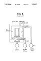
- JP OPI Publication No. 58-207050/1983 discloses a technique for forming a photoreceptor, in which, after completing a coating process in a coating method such as a dip-coating, a spray-coating, a spin-coating, a spinner-coating or a blade-coating method by making use of an apparatus such as shown in FIG. 3, the coated substratum is then dried with hot air, so that a photoreceptor can be formed.
- the specification of this patent publication gives the examples of photoreceptors each comprising a photoreceptive layer having a layer structure multilayered with a carrier generation layer and a carrier transport layer. In the examples, each of the layers are dried up with hot air at a temperature of 130° C.
- the electrophotographic characteristics are deteriorated, because a thin-coated layer such as an under layer or a carrier generation layer is so fatigued as to be deteriorated by an excess drying treatment and a heat treatment.
- a coating unevenness produced in a coating process and dispersed-grain flocculates are rapidly dried-and-fixed without any spare time to deflocculate them, so that there raise the problems that any uniform image cannot be produced because of a charging unevenness and photosensitivity unevenness produced in forming an image.
- This invention is proposed upon taking the above-described situations into consideration.
- an object of the invention to propose a process for preparing an electrophotographic photoreceptor from which any electrophotographic characteristic defects such as charging unevennness and photosensitivity unevennes can be eliminated by making no use of hot-air drying treatment when forming a thin-layer such as a carrier generation layer and after completing a coating treatment.
- FIG. 1 illustrates the steps for processing a carrier generation layer
- FIG. 2 is a block diagram illustrating the processing steps
- FIG. 3 is a cross-sectional view of a conventional dryer
- a process for preparing an electrophotographic photoreceptor comprising a step of forming plural coated layers containing a carrier generation layer on a substratum, wherein at least the above-mentioned carrier generation layer is formed on the substratum in the manner that, after the substratum is dipped and the carrier generation layer is coated thereon, the layer-coated substratum is passed through a transport step having almost the same temperature as that of the coating solution.
- a carrier generation layer in the manner that, after the foregoing substratum is dipped in a coating solution being kept at a temperature lower than 30° C. and at least a carrier generation layer is then coated thereon so as to have a wet-layer thickness within the range of 5 to 50 ⁇ m, the resulting layer-coated substratum is passed through a transport step having a temperature of the coating solution temperature ⁇ 5° C. for a period within the range of 1 to 20 minutes and, particularly that, after the foregoing substratum is dipped in a coating solution being kept at a temperature not higher than 27° C. and the carrier generation layer is then coated thereon, the resulting layer-coated substratum is passed through a transport step having a temperature of the coating solution temperature ⁇ 2° C.
- an under layer is provided, if required, onto a cylindrical substratum, and a carrier generation layer and a carrier transport layer are then coated thereon. If further required, a protective layer may be provided thereon.
- the above-mentioned cylindrical substrata include, for example; a conductive substratum vapor-deposited on a plastic cylinder surface with a metal or provided thereon with a carbon-black resin layer; and a substratum made of a metal such as aluminium, copper, steel, stainless steel, pyrites and brass.
- the particularly preferable include, for example an aluminium-made cylinder having a thickness within the range of 0.5 to 3.0 mm.
- the under layer which may be used if required is to have both functions, namely, a barrier function and an adhesion function of a substratum to a photoreceptive layer.
- the under layer include, for example, a thin layer having a thickness within the range of 0.1 to 5.0 ⁇ m and mainly comprising a macromolecular compound such as casein, polyvinyl alcohol, ethyl cellulose, carboxymethyl cellulose, nitrocellulose, an ethylene-acrylic acid copolymer, an ethylene-vinyl acetate copolymer, a vinyl chloride-vinyl acetate-maleic anhydride copolymer and Nylon.
- a macromolecular compound such as casein, polyvinyl alcohol, ethyl cellulose, carboxymethyl cellulose, nitrocellulose, an ethylene-acrylic acid copolymer, an ethylene-vinyl acetate copolymer, a vinyl chloride-vinyl acetate-maleic anhydride copolymer and Nylon.
- the above-mentioned under layer is so coated as to have a wet-thickness within the range of 1 to 50 ⁇ m onto a cylindrical substratum having been cleaned in advance by washing it well with a solvent such as dichloroethylene, trichloroethylene and chloroform in the following manner.
- the cleaned substratum is dipped in an under layer-coating solution having been prepared in advance by dissolving the aforementioned macromolecular compounds into an alcohol type solvent such as methanol, ethanol and isopropanol or a ketone type solvent such as acetone and methylethyl ketone and being kept at a temperature lower than 30° C. and preferably at a temperature not higher than 27° C.
- the above-mentioned under layer may be dried up at a relatively little higher temperature within the range of 30° C. to 60° C. if occasion requires.
- a carrier generation layer is provided, onto the above-mentioned under layer, so as to be a thin layer having a thickness within the range of 0.1 to 2 ⁇ m which is prepared by dipping a substratum coated thereon with the under layer into a coating solution comprising, for example, a resin dispersed solution containing an inorganic pigment such as photoconductive zinc oxide and cadmium sulfide, a resin dispersed solution containing an organic pigment such as a phthalocyanine type pigment, a polycyclic quinone type pigment, a perylene pigment, an azo type pigment and a quinacridone type pigment and, besides the above, a solution dispersed therein with an eutectic complex of a pyrylium salt type dye and polycarbonate.
- a coating solution comprising, for example, a resin dispersed solution containing an inorganic pigment such as photoconductive zinc oxide and cadmium sulfide, a resin dispersed solution containing an organic pigment such as
- the above-mentioned carrier generation layer can be prepared in the following manner.
- a substratum having thereon an under layer is dipped in a coating solution being kept at a temperature lower than 30° C. and preferably not higher than 27° C. under the foregoing specific clean-air atmospheric conditions and it is successively transported through the above-mentioned clean-air atmosphere for a period within the range of 1 to 20 minutes.
- a carrier generation layer it is inevitable requirement that the carrier generation layer should be transported through the above-mentioned clean-air atmosphere after it was coated.
- the coating solution is preferable to be kept at a temperature lower than 30° C. and, particularly, within the range of 27° C. to 5° C. If the temperature of the coating solution is not lower than 30° C., the liquid thickness of the upper portion becomes different from that of the lower portion thereof, that is not desirable, because, when a substratum is pulling up from a coating solution after it was dipped therein, the coating solution is flowed down rapidly. In the case of a carrier generation layer, it is attended by such an ill effect that dispersed grains are liable to flocculate. From the above-mentioned viewpoints, the coating solution temperature is preferably kept at 27° C. or lower.
- a clean-air temperature is to be nearly the same as a coating solution temperature and, if there is a big difference between the two temperatures, it is also not desirable because bubbles are so produced as to derive a coating unevenness therefrom or a back-stain is produced by a solution which invades inside of a cylindrical substratum.
- the clean-air temperature is to be within the range of a coating solution temperature ⁇ 5° C. and, preferably, a coating solution temperature ⁇ 2° C.
- the cleanness degrees of the clean-air are expressed by the number of dust grains contained in a ft 3 and they are measure by a dust-counter, Model KC-01B manufactured by Rion Co.
- the wet layer thickness L resulted by the above-mentioned dipping and coating operations can be calculated out of the following formula into which a dried layer thickness d ( ⁇ m) of each layer and the formula of a coating solution are applied. ##EQU1##
- the binder resins capable of dispersing carrier generation substances may each be selected from a wide range of insulating resins, namely, an organic photoconductive polymers such as poly-N-vinyl carbazole, polyvinyl anthracene and polyvinyl pyrene and, preferably, an insulating resin such as polystyrene, polyvinyl butyral, polyacrylate (e.g., a condensed polymer of bisphenol A and phthalic acid), polycarbonate, polyester, phenoxy resin, polyvinyl acetate, acrylic resin, polyacrylamide resin, polyamide, polyvinyl pyridine, a cellulose type resin, urethane resin, epoxy resin, casein, polyvinyl alcohol and polyvinyl pyrrolidone.
- an organic photoconductive polymers such as poly-N-vinyl carbazole, polyvinyl anthracene and polyvinyl pyrene
- an insulating resin such as polystyrene, polyviny
- the organic solvents applicable to prepare a coating solution include, for example, the following compounds;
- Alcohols such as methanol, ethanol and isopropanol; ketones such as acetone, methylethyl ketone and cyclohexanone; amides such as N,N-dimethyl formamide and N,N-dimethyl acetamide; sulfoxides such as dimethyl sulfoxide; ethers such as tetrahydrofran, dioxane and ethylene glycol monomethyl ether; esters such as methyl acetate and ethyl acetate; aliphatic halogenohydrocarbons such as chloroform, methylene chloride, dichlorethylene, carbon tetrachloride and trichlorethylene; or aromatic compounds such as benzene, toluene, xylene, ligroin, monochlorobenzene and dichlorobenzene.
- ketones such as acetone, methylethyl ketone and cyclohexanone
- amides such as N,
- a carrier transport layer to be formed on the above-mentioned carrier generation layer can be formed in the following manner.
- a substratum having thereon the foregoing under layer and carrier generation layer is dipped in and then coated thereon with a coating solution comprising a resin solution containing the following carrier transport substances, and finally dried.
- the carrier transport substances include, for example, an oxazole derivative, an oxadiazole derivative, a thiazole derivative, a thiadiazole derivative, a triazole derivative, an imidazole derivative, an imidazolone derivative, an imidazolidine derivative, a bisimidazolidine derivative, a styryl compound, a hydrazone compound, a pyrazoline derivative, an amine derivative, an oxazolone derivative, a benzothiazole derivative, a benzimidazole derivative, a quinazoline derivative, a benzfran derivative, an acridine derivative, a phenadine derivative, an aminostilbene derivative, poly-N-vinyl carbazole, poly-1-vinyl pyrene and poly-9-vinyl anthracene.
- the above-mentioned carrier transport layer is dipped in a clean-air atmosphere as same as in the cases of the under layer and the carrier generation layer and is then so coated as to have a wet-layer thickness within the range of 50 to 100 ⁇ m and, thereafter, it is dried up in a hot-air atmosphere having a temperature within the range of 80° to 150° C. for a period within the range of 30 to 90 minutes.
- a photoreceptor comprising a laminated photoreceptive layer having a finished layer thickness within the range of 10 to 30 ⁇ m and preferably 15 to 25 ⁇ m can be prepared.
- the binder resins applicable to the above-mentioned carrier transport layer coating solution the resins similar to those applicable to the foregoing carrier generation layer can be used. However, the resins compatible to the applicable carrier transport substances are to be selected out.
- the solvents applicable to the carrier transport layer the solvents applicable to the foregoing carrier generation layer may be appropriated thereto. However, the solvents capable of dissolving the above-mentioned carrier transport substances and the binder resins thereof are to be used.
- a protective layer having a layer thickness within the range of 0.01 to 1.0 ⁇ m may be arranged over to the foregoing support, if required. If this is the case, it is usually desirable to produce the protective layer, in the same manner as in the foregoing under layer formation, by dipping and coating it in the clean-air atmosphere and then by passing it through the transport step under the same clean-air atmosphere.
- FIG. 1 shows an example of the coating.transporting step carried out in a method of dipping.coating a cylindrical substratum in a carrier generation layer coating solution.
- (I) shows the step for pretreating a carrier generation layer which is not yet coated, that is, the step for washing.drying substratum Ia or for coating transporting (or drying) an under layer;
- (II) shows the step for coating the carrier generation layer;
- (III) shows the step for transporting the carrier generation layer which was already coated; and
- (IV) shows the successive step for processing a carrier transport layer.
- Substratum I is transported by, for example, a robot, between each of the steps while supporting it on support.transport tables 2a and 2b.
- the substratum is transported as shown by 1 b from the preceding step (I) into the step (II) for coating a carrier generation layer while being supported on transport table 2a and is then retained by DRUM SUPPORT CHUCK 4 hung from ceiling 14 so as to be lifted up once while keeping one of the open ends closed. Then, after returning transport table 2a back to step (I), the substratum is dipped in coating solution tank 5, so that the coating solution can be coated thereon.
- the coating solution stored in the coating solution tank is kept at a specific temperature by heat-retaining water circulated by pump 9 from thermostat water tank 7 to the space between solution tank 5 and outer wall 6 thereof, and outer wall 6 of solution tank 5 is kept at a constant temperature by heat-retaining jacket 8.
- the coating solution stored in the above-mentioned solution tank 5 is introduced from coating solution replenisher tank 16 placed under floor 15 through coating solution transport pipe 20 attached with pump 17 and filter 18 so as to be overflowed into solution reservoir 5a when substratum 1b is dipped in solution tank 5.
- the overflow is collected and returned to the above-mentioned solution tank 16 through pipe 19, and solution tank 16 is kept at a specific temperature by jacket 21.
- An under layer coating solution was prepared by dissolving 100 g of a vinyl chloride-vinyl acetate-maleic anhydride copolymer (Eslec MF-10 manufactured by Sekisui Chemical Co.) in 10000 ml of acetone and the resulting solution was then adjusted to have a temperature of 25° C.
- a vinyl chloride-vinyl acetate-maleic anhydride copolymer (Eslec MF-10 manufactured by Sekisui Chemical Co.)
- a carrier generation layer coating solution was prepared in the following manner,
- the above-mentioned under layer was processed in common in accordance with block diagrams B1, B2 and B3.
- the resulting under layer-coated substrata were each transported to the successive carrier generation layer processing step.
- the carrier generation layer was processed in a coating step under the clean-air atmosphere similar to the case of the above-described under layer.
- B1, B2 and B3 were processed in common processing steps.
- the photoreceptors (Nos. 1, 3, 4, 5, 7, 8, 9, 11 and 12), which were each applied with a substratum having a diameter of 80 mm ⁇ , A1, A3 and A4, were loaded on U-Bix 2025; and the photoreceptors (Nos. 2, 6 and 10), which were each applied with a substratum A2 having a diameter of 60 mm ⁇ , were loaded on U-Bix 1515.
- the photoreceptors for testing the invention (Nos. 1, 3, 4, 5, 7 and 8) and those for testing the comparison (Nos. 9, 11 and 12) were each loaded on U-Bix 2025, and the photoreceptors for testing the invention (Nos. 2 and 6) and that for testing the comparison (No. 10) was loaded on U-Bix 1515.
- Each of the image formation was tried by making use of a solid black original under the atmospheric conditions of 20° C. and RH60%, so that the image qualities of the resulting solid black images could be evaluated. The results thereof are shown in Table 3 given below.
- a photoreceptor can be provided so that a high density and sharp image can stably be obtained to have excellent electrophotographic characteristics without having any image unevenness.
- the other advantages can also be displayed, for example, the photoreceptor can effectively be prepared with low cost and excellent productivity.
Landscapes
- Physics & Mathematics (AREA)
- General Physics & Mathematics (AREA)
- Photoreceptors In Electrophotography (AREA)
Abstract
A process of preparing electrophotographic photoreceptor aluminum drums having coated layers with a constant thickness and properties is disclosed. After a carrier generation layer being dip coated, a process of conveyance is followed at a temperature same as that of the coating material.
Description
This invention relates to a process for preparing an electrophotographic photoreceptor in which a photoreceptive layer is formed on, for example, a cylindrical substratum, in a dip-coating method.
Japanese Patent Publication Open to Public Inspection--hereinafter referred to as `JP OPI Publication- No. 61-149272/1986`, for example, has so far proposed a technique relating to the preparation of an electrophotographic photoreceptor, in which a coating solution containing a photoconductive composite is coated on a cylindrical substratum in a dip-coating method.
In the above patent publication, a substratum having one end closed and the other end opened has been used as a cylindrical substratum. When the substratum is coated by dipping it in a coating solution from its open end, the patent publication describes that it would be preferred to keep a coating room temperature TA (or the air temperature of the substratum) equivalent to or relatively little higher than a coating solution temperature TL. For example, it describes that, if a substratum thickness is not thinner than 1 mm, the relation between the two temperatures is preferably -2° C.≦TA -TL ≦10° C. and, if a substratum thickness is not thicker than 1 mm, the relation therebetween is preferably -1° C.≦TA -TL ≦3° C. The proposal of the above patent publication paid attention to the temperature characteristics when a substratum is coated. However, post-process treatments to be made after completing a coating process are also very important from the viewpoint of preparing an electrophotographic photoreceptor.
Therefore, JP OPI Publication No. 58-207050/1983 discloses a technique for forming a photoreceptor, in which, after completing a coating process in a coating method such as a dip-coating, a spray-coating, a spin-coating, a spinner-coating or a blade-coating method by making use of an apparatus such as shown in FIG. 3, the coated substratum is then dried with hot air, so that a photoreceptor can be formed. The specification of this patent publication gives the examples of photoreceptors each comprising a photoreceptive layer having a layer structure multilayered with a carrier generation layer and a carrier transport layer. In the examples, each of the layers are dried up with hot air at a temperature of 130° C.
However, in the above-mentioned preparation processes carried out with such a hot air-drying treatment as described above, the electrophotographic characteristics are deteriorated, because a thin-coated layer such as an under layer or a carrier generation layer is so fatigued as to be deteriorated by an excess drying treatment and a heat treatment. In the case of a carrier generation layer, a coating unevenness produced in a coating process and dispersed-grain flocculates are rapidly dried-and-fixed without any spare time to deflocculate them, so that there raise the problems that any uniform image cannot be produced because of a charging unevenness and photosensitivity unevenness produced in forming an image.
This invention is proposed upon taking the above-described situations into consideration.
It is, accordingly, an object of the invention to propose a process for preparing an electrophotographic photoreceptor from which any electrophotographic characteristic defects such as charging unevennness and photosensitivity unevennes can be eliminated by making no use of hot-air drying treatment when forming a thin-layer such as a carrier generation layer and after completing a coating treatment.
FIG. 1 illustrates the steps for processing a carrier generation layer;
FIG. 2 is a block diagram illustrating the processing steps; and
FIG. 3 is a cross-sectional view of a conventional dryer; wherein
1a, 1b, 1c . . . Substratum;
2a, 2b . . . Support carrier tables;
4 . . . DRUM SUPPORT CHUCK;
5 . . . Coating solution tank;
7 . . . Thermostat water tank;
12a, 12b, 12c, 12d . . . AIR FILTER;
16 . . . Coating replenisher tank;
18 . . . FILTER FOR Coating Solution
The aforementioned objects of the invention can be achieved with a process for preparing an electrophotographic photoreceptor comprising a step of forming plural coated layers containing a carrier generation layer on a substratum, wherein at least the above-mentioned carrier generation layer is formed on the substratum in the manner that, after the substratum is dipped and the carrier generation layer is coated thereon, the layer-coated substratum is passed through a transport step having almost the same temperature as that of the coating solution.
In the preferable embodiments of the preparation processes of the invention, it is preferred to form a carrier generation layer in the manner that, after the foregoing substratum is dipped in a coating solution being kept at a temperature lower than 30° C. and at least a carrier generation layer is then coated thereon so as to have a wet-layer thickness within the range of 5 to 50 μm, the resulting layer-coated substratum is passed through a transport step having a temperature of the coating solution temperature ±5° C. for a period within the range of 1 to 20 minutes and, particularly that, after the foregoing substratum is dipped in a coating solution being kept at a temperature not higher than 27° C. and the carrier generation layer is then coated thereon, the resulting layer-coated substratum is passed through a transport step having a temperature of the coating solution temperature ±2° C.
It is usual in the preparation processes of the invention that an under layer is provided, if required, onto a cylindrical substratum, and a carrier generation layer and a carrier transport layer are then coated thereon. If further required, a protective layer may be provided thereon.
The above-mentioned cylindrical substrata include, for example; a conductive substratum vapor-deposited on a plastic cylinder surface with a metal or provided thereon with a carbon-black resin layer; and a substratum made of a metal such as aluminium, copper, steel, stainless steel, pyrites and brass. The particularly preferable include, for example an aluminium-made cylinder having a thickness within the range of 0.5 to 3.0 mm. The under layer which may be used if required is to have both functions, namely, a barrier function and an adhesion function of a substratum to a photoreceptive layer. The under layer include, for example, a thin layer having a thickness within the range of 0.1 to 5.0 μm and mainly comprising a macromolecular compound such as casein, polyvinyl alcohol, ethyl cellulose, carboxymethyl cellulose, nitrocellulose, an ethylene-acrylic acid copolymer, an ethylene-vinyl acetate copolymer, a vinyl chloride-vinyl acetate-maleic anhydride copolymer and Nylon.
The above-mentioned under layer is so coated as to have a wet-thickness within the range of 1 to 50 μm onto a cylindrical substratum having been cleaned in advance by washing it well with a solvent such as dichloroethylene, trichloroethylene and chloroform in the following manner. The cleaned substratum is dipped in an under layer-coating solution having been prepared in advance by dissolving the aforementioned macromolecular compounds into an alcohol type solvent such as methanol, ethanol and isopropanol or a ketone type solvent such as acetone and methylethyl ketone and being kept at a temperature lower than 30° C. and preferably at a temperature not higher than 27° C. so that the substratum can be so coated as to have the above-mentioned wet-thickness. The dip-coating step is performed under the specific clean-air atmospheric conditions of a coating solution temperature of ±5° C. and preferably ±2° C. and under the atmospheric conditions of a cleanness degree of not higher than 100. After completing the coating treatment, the coated substratum is transported through the above-mentioned clean-air atmospheric conditions for a period within the range of 1 to 20 minutes and is then followed into the successive step of coating a carrier generation layer.
The above-mentioned under layer may be dried up at a relatively little higher temperature within the range of 30° C. to 60° C. if occasion requires.
A carrier generation layer is provided, onto the above-mentioned under layer, so as to be a thin layer having a thickness within the range of 0.1 to 2 μm which is prepared by dipping a substratum coated thereon with the under layer into a coating solution comprising, for example, a resin dispersed solution containing an inorganic pigment such as photoconductive zinc oxide and cadmium sulfide, a resin dispersed solution containing an organic pigment such as a phthalocyanine type pigment, a polycyclic quinone type pigment, a perylene pigment, an azo type pigment and a quinacridone type pigment and, besides the above, a solution dispersed therein with an eutectic complex of a pyrylium salt type dye and polycarbonate.
The above-mentioned carrier generation layer can be prepared in the following manner. A substratum having thereon an under layer is dipped in a coating solution being kept at a temperature lower than 30° C. and preferably not higher than 27° C. under the foregoing specific clean-air atmospheric conditions and it is successively transported through the above-mentioned clean-air atmosphere for a period within the range of 1 to 20 minutes. In the case of a carrier generation layer, it is inevitable requirement that the carrier generation layer should be transported through the above-mentioned clean-air atmosphere after it was coated.
The reason why the above-mentioned transportation should be inevitable is that dispersed grains, i.e., carrier generation substances, are liable to flocculate in a coating solution layer in a coating step. Therefore, when the above-mentioned coating solution layer is passed through an atomosphere having a temperature nearly the same as the temperature of the coating solution, after completing the coating step, the flocculation is dispersed to be deflocculated, so that a photoreceptor without having any charging unevennes and photosensitivity unevenness; can be obtained.
The coating solution is preferable to be kept at a temperature lower than 30° C. and, particularly, within the range of 27° C. to 5° C. If the temperature of the coating solution is not lower than 30° C., the liquid thickness of the upper portion becomes different from that of the lower portion thereof, that is not desirable, because, when a substratum is pulling up from a coating solution after it was dipped therein, the coating solution is flowed down rapidly. In the case of a carrier generation layer, it is attended by such an ill effect that dispersed grains are liable to flocculate. From the above-mentioned viewpoints, the coating solution temperature is preferably kept at 27° C. or lower. When the temperature thereof is lower than 5° C., the solution temperature is too low to obtain any uniformly coated layer. It is also preferable that a clean-air temperature is to be nearly the same as a coating solution temperature and, if there is a big difference between the two temperatures, it is also not desirable because bubbles are so produced as to derive a coating unevenness therefrom or a back-stain is produced by a solution which invades inside of a cylindrical substratum.
From the reasons mentioned above, the clean-air temperature is to be within the range of a coating solution temperature ±5° C. and, preferably, a coating solution temperature ±2° C.
The cleanness degrees of the clean-air are to be preferably not higher than 100. If the cleaness degrees exceed 100, it is not desirable because spots are produced. The cleaness degrees of clean-air can be measured in the following manner.
The cleanness degrees of the clean-air are expressed by the number of dust grains contained in a ft3 and they are measure by a dust-counter, Model KC-01B manufactured by Rion Co.
The number of the above-mentioned dust grains can be measured by specifying the grain sizes, namely, not smaller than 0.1 μm, not smaller than 0.3μm and not smaller than 0.5 μm. In the invention, the cleannes degrees are measured by the numbers of the above-mentioned dust grains each having the grain sizes not smaller than 0.5 μm.
The wet layer thickness L resulted by the above-mentioned dipping and coating operations can be calculated out of the following formula into which a dried layer thickness d (μm) of each layer and the formula of a coating solution are applied. ##EQU1##
In the above-mentioned carrier generation layer, the binder resins capable of dispersing carrier generation substances may each be selected from a wide range of insulating resins, namely, an organic photoconductive polymers such as poly-N-vinyl carbazole, polyvinyl anthracene and polyvinyl pyrene and, preferably, an insulating resin such as polystyrene, polyvinyl butyral, polyacrylate (e.g., a condensed polymer of bisphenol A and phthalic acid), polycarbonate, polyester, phenoxy resin, polyvinyl acetate, acrylic resin, polyacrylamide resin, polyamide, polyvinyl pyridine, a cellulose type resin, urethane resin, epoxy resin, casein, polyvinyl alcohol and polyvinyl pyrrolidone.
The organic solvents applicable to prepare a coating solution include, for example, the following compounds;
Alcohols such as methanol, ethanol and isopropanol; ketones such as acetone, methylethyl ketone and cyclohexanone; amides such as N,N-dimethyl formamide and N,N-dimethyl acetamide; sulfoxides such as dimethyl sulfoxide; ethers such as tetrahydrofran, dioxane and ethylene glycol monomethyl ether; esters such as methyl acetate and ethyl acetate; aliphatic halogenohydrocarbons such as chloroform, methylene chloride, dichlorethylene, carbon tetrachloride and trichlorethylene; or aromatic compounds such as benzene, toluene, xylene, ligroin, monochlorobenzene and dichlorobenzene.
Next, a carrier transport layer to be formed on the above-mentioned carrier generation layer can be formed in the following manner. A substratum having thereon the foregoing under layer and carrier generation layer is dipped in and then coated thereon with a coating solution comprising a resin solution containing the following carrier transport substances, and finally dried. The carrier transport substances include, for example, an oxazole derivative, an oxadiazole derivative, a thiazole derivative, a thiadiazole derivative, a triazole derivative, an imidazole derivative, an imidazolone derivative, an imidazolidine derivative, a bisimidazolidine derivative, a styryl compound, a hydrazone compound, a pyrazoline derivative, an amine derivative, an oxazolone derivative, a benzothiazole derivative, a benzimidazole derivative, a quinazoline derivative, a benzfran derivative, an acridine derivative, a phenadine derivative, an aminostilbene derivative, poly-N-vinyl carbazole, poly-1-vinyl pyrene and poly-9-vinyl anthracene.
The above-mentioned carrier transport layer is dipped in a clean-air atmosphere as same as in the cases of the under layer and the carrier generation layer and is then so coated as to have a wet-layer thickness within the range of 50 to 100 μm and, thereafter, it is dried up in a hot-air atmosphere having a temperature within the range of 80° to 150° C. for a period within the range of 30 to 90 minutes. Thereby, a photoreceptor comprising a laminated photoreceptive layer having a finished layer thickness within the range of 10 to 30 μm and preferably 15 to 25 μm can be prepared.
As for the binder resins applicable to the above-mentioned carrier transport layer coating solution, the resins similar to those applicable to the foregoing carrier generation layer can be used. However, the resins compatible to the applicable carrier transport substances are to be selected out. As for the solvents applicable to the carrier transport layer, the solvents applicable to the foregoing carrier generation layer may be appropriated thereto. However, the solvents capable of dissolving the above-mentioned carrier transport substances and the binder resins thereof are to be used.
Further, a protective layer having a layer thickness within the range of 0.01 to 1.0 μm may be arranged over to the foregoing support, if required. If this is the case, it is usually desirable to produce the protective layer, in the same manner as in the foregoing under layer formation, by dipping and coating it in the clean-air atmosphere and then by passing it through the transport step under the same clean-air atmosphere.
FIG. 1 shows an example of the coating.transporting step carried out in a method of dipping.coating a cylindrical substratum in a carrier generation layer coating solution. In the figure, (I) shows the step for pretreating a carrier generation layer which is not yet coated, that is, the step for washing.drying substratum Ia or for coating transporting (or drying) an under layer; (II) shows the step for coating the carrier generation layer; (III) shows the step for transporting the carrier generation layer which was already coated; and (IV) shows the successive step for processing a carrier transport layer. Substratum I is transported by, for example, a robot, between each of the steps while supporting it on support.transport tables 2a and 2b. To each of the steps, the clean-air is introduced through duct 13 equipped with air-conditioner 10, fan 11 and each of filters 12a, 12b, 12c and 12d. The clean-air with a solvent is exhausted from ducts 14a and 14b and, at this time, each of the steps is retained on the clean-air pressure side so that any dusts invading from outside can be prevented. In this figure, a cylindrical substratum having both of the opened ends is shown, in which a coating solution is coated on the substratum in the following manner. The substratum is transported as shown by 1 b from the preceding step (I) into the step (II) for coating a carrier generation layer while being supported on transport table 2a and is then retained by DRUM SUPPORT CHUCK 4 hung from ceiling 14 so as to be lifted up once while keeping one of the open ends closed. Then, after returning transport table 2a back to step (I), the substratum is dipped in coating solution tank 5, so that the coating solution can be coated thereon. The coating solution stored in the coating solution tank is kept at a specific temperature by heat-retaining water circulated by pump 9 from thermostat water tank 7 to the space between solution tank 5 and outer wall 6 thereof, and outer wall 6 of solution tank 5 is kept at a constant temperature by heat-retaining jacket 8.
The coating solution stored in the above-mentioned solution tank 5 is introduced from coating solution replenisher tank 16 placed under floor 15 through coating solution transport pipe 20 attached with pump 17 and filter 18 so as to be overflowed into solution reservoir 5a when substratum 1b is dipped in solution tank 5. The overflow is collected and returned to the above-mentioned solution tank 16 through pipe 19, and solution tank 16 is kept at a specific temperature by jacket 21.
The above-mentioned substratum 1b is dipped in coating solution tank 5 and is then pulled up therefrom. After substratum 1b is released from chuck 4, it is placed on empty transport table 2b transported from succesive transport step (III). It is transported, in the form of substratum 1c retaining a carrier generation layer, into transport step (III) for a period within the range of 1 to 20 minutes and is then transported into seccessive step (IV).
The carrier generation layer has been described as an example. Also in the cases of an under layer and a protective layer each provided if required, it is preferred to use the same steps. When taking the above-described preparation steps, a photoreceptor can be prepared so as to have uniform and unscattered electrophotographic characteristics.
The invention will now be detailed with reference to the examples thereof. It is, however, to be understood that the embodiments of the invention shall not be limited thereto.
First, 12 pieces of cold-drawn aluminium-matrix pipes having the following dimensions were each surface-treated as shown in Table 1 so that 3 pieces each of 4 kinds of substrata, A1, A2, A3 and A4, totaling 12 pieces could be prepared.
                                  TABLE 1
__________________________________________________________________________
          Outer diameter
                   Length of pipe l
                             Thickness t      Surface roughness
                                                        Number
Dimensions, etc.
          (mm)     (mm)      (mm)   Surface treated
                                              Rmax (mm) of
__________________________________________________________________________
                                                        pipes
Substrata
A1        80.0     355.5     1.25   Mirror-finished
                                              0.2       3
                                    with a single
                                    crystal diamond
                                    bite
A2        80.0     351.0     1.00   Mirror-finished
                                              0.2       3
                                    with a single
                                    crystal diamond
                                    bite
A3        80.0     355.5     1.25   Processed with
                                              0.8       3
                                    a grindstone
A4        80.0     355.5     1.25   Processed with
                                              0.8       3
                                    a polycrystal
                                    diamond bite
__________________________________________________________________________
(2-1) Under layer coating solution
An under layer coating solution was prepared by dissolving 100 g of a vinyl chloride-vinyl acetate-maleic anhydride copolymer (Eslec MF-10 manufactured by Sekisui Chemical Co.) in 10000 ml of acetone and the resulting solution was then adjusted to have a temperature of 25° C.
(2-2) Carrier generation layer coating solution
A carrier generation layer coating solution was prepared in the following manner,
______________________________________
A dibromoanthoanthrone pigment,
                         200 g
(Monolite-Red 2Y manufactured by ICI)
                         and
A polycarbonate resin, (Panlite L-1250
                         100 g
manufactured by Teijin Chemical Co.)
______________________________________
were each dissolved and dispersed in 8700 ml of 1,2-dichlorethane and the resulting solution was then so adjusted as to have a temperature of 25° C.
(2-3) Carrier Transport Layer Coating Solution
A carrier transport layer coating solution was prepared in the following manner, ##STR1## were each dissolved in 7800 ml of 1,2-dichlorethane and the resulting solution was so adjusted as to have a temperature of 25° C.
The 4 kinds of substrata, A1 through A4 shown in the foregoing table 1, were each dipped in trichlorethane having a temperature of 40° C. and they were shaken and stirred by a supersonic stirrer at 28 KHz for 120 seconds. The temperatures thereof were cooled down to 25° C. and they were shaked and stirred again by the stirrer at 40 KHz for 60 seconds and then washed. Finally, they were further washed with trichlorethan vapor at 74° C. and dried up, so that 4 kind totaling 12 pieces (i.e., 3 pieces per kind) of substrata subject to photoreceptive layer coating could be obtained.
The photoreceptors subject to the tests No. 1 through No. 12 (among which test Nos. 1 to 8 were each for testing the inventive photoreceptors and test Nos. 9 to 12 were each for testing the comparative photoreceptors) could be each prepared by coating thereon with the foregoing coating solutions, respectively, by making use of the resulting substrata and according to block diagrams B1 and B2 for testing the inventive photoreceptors and block diagram B3 for testing the comparative photoreceptors; each of the diagrams shown in FIG. 2, illustrating the steps for preparing photoreceptors.
TABLE 2 ______________________________________ Substratum A1 A2 A3 A4 ______________________________________ Photoreceptor No. Preparing step Forinventive test B1 1 2 3 4 B2 5 6 7 8 For comparative test B3 9 10 11 12 ______________________________________
The above-mentioned under layer was processed in common in accordance with block diagrams B1, B2 and B3. The washed substrata were each dipped in a coating solution being kept at a temperature of 25° C. under the clean-air atmospheric conditions at 25° C., RH35% and class 100 and pulled up at a pulling-up rate S1 of S1 =10 mm/sec., so that the substrata could be so coated as to have a wet-layer thickness of 7 μm. In processing step B1, the substrata were each transported under the foregoing clean-air atmosphere for a transporting time t4 =10 minutes after they were each coated, so that an under layer could have a layer thickness of 0.5 μm. The resulting under layer-coated substrata were each transported to the successive carrier generation layer processing step.
In processing steps B2 and B3, the substrata were each coated and were then dried up (i.e., primarily dried up) by hot-air having a drying temperature T1 =40° C. for a drying time T1 =15 minutes, so that the substrata were each transported to the successive carrier generation layer processing step.
In each of the processing steps B1, B2 and B3, the carrier generation layer was processed in a coating step under the clean-air atmosphere similar to the case of the above-described under layer. In processing steps B1 and B2, the substrata each having an under layer were dipped in a coating solution being kept at a temperature of 25° C. and were then pulled up at a pulling-up rate of S2 =8 mm/sec., so that they were each so coated as to have a wet-layer thickness of 4 μm. In processing step B3, the substrata were each dipped in a coating solution being kept at a temperature of 30° C. and were then pulled up at a pulling-up rate of S3 =6 mm/sec., so that they were each so coated as to have a wet-layer thickness of 4 μm.
In processing steps B1 and B2 after completing the coating treatments, a carrier generation layer having a little thicker than 1.0 μm thickness could be obtained upon transporting a substratum under the above-mentioned clean-air atmosphere for a transport time of t5 =10 minutes. In processing step B3, a 1.0 μm-thick carrier generation layer could be obtained upon drying it with hot-air having a drying temperature of T2 =85° C. for a drying time of t2 =30 minutes and it was then transported to the successive carrier transport layer processing step.
For the layers following the carrier transport layer, B1, B2 and B3 were processed in common processing steps.
A carrier transport layer was coated also in such a manner that a substratum having an under layer and a carrier generation layer was dipped in a coating solution kept at 25° C. under the clean-air atmosphere as same as in coating the under layer and the substratum was pulled up from the coating solution at the pulling-up rate of S2 =2.5 mm/sec., so that a coating solution layer having a wet-thickness of 90 μm could be obtained. In each of the processing steps, B1, B2 and B3 shown in FIG. 2, the photoreceptor comprising a photoreceptive layer having a dried-thickness of 20 μm could be prepared by carrying out a predrying of T3 =70° C. for 15 minutes and a principal drying of T3 =85° C. for 45 minutes.
Electrostatic characteristics measurement:
Among the resulting 12 kinds of photoreceptors, the photoreceptors, (Nos. 1, 3, 4, 5, 7, 8, 9, 11 and 12), which were each applied with a substratum having a diameter of 80 mmφ, A1, A3 and A4, were loaded on U-Bix 2025; and the photoreceptors (Nos. 2, 6 and 10), which were each applied with a substratum A2 having a diameter of 60 mmφ, were loaded on U-Bix 1515. To the developing position was arranged with a potentiometric probe, an electrostatic meter and a recorder, so that the resulting black-paper potential VB volt, the white-paper potential VW volt and dark decay ration 30 seconds after charging D% could be measured. The results thereof are shown in Table 3.
Practical copying test:
Similar to the case of the above-described electrostatic characteristics measurement, the photoreceptors for testing the invention (Nos. 1, 3, 4, 5, 7 and 8) and those for testing the comparison (Nos. 9, 11 and 12) were each loaded on U-Bix 2025, and the photoreceptors for testing the invention (Nos. 2 and 6) and that for testing the comparison (No. 10) was loaded on U-Bix 1515. Each of the image formation was tried by making use of a solid black original under the atmospheric conditions of 20° C. and RH60%, so that the image qualities of the resulting solid black images could be evaluated. The results thereof are shown in Table 3 given below.
                                  TABLE 3
__________________________________________________________________________
                      Electrostatic characteristics
                                               Practical photorecording
                                               test
Test No.  Processing  Black-paper
                               Dark-decay
                                      White-paper
                                               Test machine
(Photoreceptor No.)
          test  Substratum
                      potential V.sub.B (V)
                               (%)    potential V.sub.W
                                               used   Image
__________________________________________________________________________
                                                      quality
Invention test
1         B1    A1    680      22.0   70       U-Bix 2025
                                                      Excellent
2         B1    A2    650      21.9   91       U-Bix 1515
                                                      Excellent
3         B1    A3    680      22.0   69       U-Bix 2025
                                                      Excellent
4         B1    A4    680      22.1   70       U-Bix 2025
                                                      Excellent
5         B2    A1    680      21.8   68       U-Bix 2025
                                                      Excellent
6         B2    A2    650      22.0   90       U-Bix 1515
                                                      Excellent
7         B2    A3    680      22.0   70       U-Bix 2025
                                                      Excellent
8         B2    A4    680      21.0   69       U-Bix 2025
                                                      Excellent
Comparison test
9         B3    A1    680      45.0   70       U-Bix 2025
                                                      Unevenly imaged
10        B3    A2    650      44.8   90       U-Bix 1515
                                                      Unevenly imaged
11        B3    A3    680      45.0   69       U-Bix 2025
                                                      Unevenly imaged
12        B3    A4    680      44.9   69       U-Bix 2025
                                                      Unevenly
__________________________________________________________________________
                                                      imaged
From the results of the electrostatic characteristics and the practical photorecording tests, it could be observed the following facts. In the tests of the invention, not only the electrostatic characteristics could be excellent, but also a high density and sharp image could be obtained without having any image unevennes. In the tests of the comparison, in contrast to the above, the electrostatic characteristics could not be excellent and, in particular, the dark decay was increased and the image density was in low and, in addition, the image unevenness were produced.
As is apparent from the above descriptions, according to the preparation process of the invention, a photoreceptor can be provided so that a high density and sharp image can stably be obtained to have excellent electrophotographic characteristics without having any image unevenness. In addition to the above, the other advantages can also be displayed, for example, the photoreceptor can effectively be prepared with low cost and excellent productivity.
Claims (8)
1. A process of producing an electrophotographic photoreceptor, the photoreceptor comprising a plurality of layers including a carrier generation layer having a thickness of 0.1 to 2 μm, comprising the steps of:
dipping a substratum into a coating solution to form the carrier generation layer thereon; and
conveying the substratum coated with the carrier generation layer under circulating clean air having a cleanness degree of not higher than 100, at a temperature in a range of plus or minus 5 centigrade degrees of the temperature of the coating solution.
2. The process of claim 1 wherein a temperature of the coating solution is less than 30° C., and the temperature of the conveying step is in the range of plus or minus 2° C. of the temperature of the coating solution.
3. The process of claim 2 wherein the temperature of the coating solution is less than 27° C., and the temperature of the conveying step is in the range of plus or minus 2° C. of the temperature of the coating solution.
4. The process of claim 1 wherein an interval of the conveying step is 1 minute to 15 minutes.
5. The process of claim 2 wherein an interval of the conveying step is 1 minute to 15 minutes.
6. The process of claim 3 wherein an interval of the conveying step is 1 minute to 15 minutes.
7. A process of producing an electrophotographic photoreceptor comprising the steps of:
(a) preparing an aluminum drum,
(b) coating an under layer on an outer surface of the aluminum drum,
(c) conveying the aluminum drum coated with the under layer to a process of coating a carrier generation layer, by a first conveyer,
(d) coating the carrier generation layer onto the aluminum drum coated with the under layer by dipping the drum into a carrier generation layer coating solution having a temperature of 5° C. to 27° C. to form a wet layer of 5 to 50 μm,
(e) conveying the aluminum drum coated with the layers to a process of coating a carrier transport layer, by a second conveyer, taking 1 to 20 minutes under circulating clean air having a cleaness degree of not higher than 100, and at a temperature of plus or minus 2° C. that of the temperature of the carrier generation layer coating solution, a carrier generation layer having a thickness of 0.1 to 2 μm being formed during conveyance,
(f) coating a wet state carrier transport layer of 50 to 100 μm onto the carrier generation layer coated on the aluminum drum,
(g) drying the carrier generation layer for 30 to 90 minutes under clean air at a temperature of 80° to 150° C. to form a carrier transport layer of 10 to 30 μm in thickness.
8. The process of claim 1 wherein the conveying step under circulating clean air is for a time interval of 1 to 20 minutes.
Applications Claiming Priority (2)
| Application Number | Priority Date | Filing Date | Title |
|---|---|---|---|
| JP2-309223 | 1990-11-15 | ||
| JP2309223A JP3010374B2 (en) | 1990-11-15 | 1990-11-15 | Manufacturing method of electrophotographic photoreceptor |
Publications (1)
| Publication Number | Publication Date |
|---|---|
| US5213937A true US5213937A (en) | 1993-05-25 |
Family
ID=17990418
Family Applications (1)
| Application Number | Title | Priority Date | Filing Date |
|---|---|---|---|
| US07/791,563 Expired - Lifetime US5213937A (en) | 1990-11-15 | 1991-11-12 | Process for preparing an electrophotographic photoreceptor |
Country Status (2)
| Country | Link |
|---|---|
| US (1) | US5213937A (en) |
| JP (1) | JP3010374B2 (en) |
Cited By (11)
| Publication number | Priority date | Publication date | Assignee | Title |
|---|---|---|---|---|
| US5476740A (en) * | 1992-08-19 | 1995-12-19 | Xerox Corporation | Multilayer electrophotographic imaging member |
| US5532103A (en) * | 1992-08-19 | 1996-07-02 | Xerox Corporation | Multilayer electrophotographic imaging member |
| US5599646A (en) * | 1996-03-29 | 1997-02-04 | Xerox Corporation | Higher substrate density dip coating method |
| US5633046A (en) * | 1995-05-22 | 1997-05-27 | Xerox Corporation | Multiple dip coating method |
| US5667928A (en) * | 1996-06-06 | 1997-09-16 | Xerox Corporation | Dip coating method having intermediate bead drying step |
| US5720815A (en) * | 1996-03-01 | 1998-02-24 | Xerox Corporation | Dip coating apparatus having solution displacement apparatus |
| US5725667A (en) * | 1996-03-01 | 1998-03-10 | Xerox Corporation | Dip coating apparatus having a single coating vessel |
| US6048658A (en) * | 1999-09-29 | 2000-04-11 | Xerox Corporation | Process for preparing electrophotographic imaging member |
| US6096470A (en) * | 1999-10-28 | 2000-08-01 | Xerox Corporation | Electrophotographic imaging member overcoat fabrication process |
| US6221436B1 (en) | 1995-08-21 | 2001-04-24 | Xerox Corporation | Coating method involving substrate cleaning |
| EP1255165A3 (en) * | 2001-05-01 | 2003-01-29 | Ricoh Company, Ltd. | Coating system and system for producing photoconductive elements for electrophotography |
Families Citing this family (3)
| Publication number | Priority date | Publication date | Assignee | Title |
|---|---|---|---|---|
| JP2007225867A (en) * | 2006-02-23 | 2007-09-06 | Ricoh Co Ltd | Electrophotographic photoreceptor coating film forming apparatus and coating film forming method, electrophotographic photoreceptor, image forming method, image forming apparatus and process cartridge using the same |
| US8066660B2 (en) | 2007-10-26 | 2011-11-29 | C. R. Bard, Inc. | Split-tip catheter including lateral distal openings |
| JP5634048B2 (en) * | 2009-11-02 | 2014-12-03 | キヤノン株式会社 | Method for producing electrophotographic photosensitive member |
Citations (2)
| Publication number | Priority date | Publication date | Assignee | Title |
|---|---|---|---|---|
| US4252883A (en) * | 1972-04-28 | 1981-02-24 | Canon Kabushiki Kaisha | Process for producing electrophotographic photosensitive member |
| US4618559A (en) * | 1984-05-17 | 1986-10-21 | Canon Kabushiki Kaisha | Process of making electrophotographic photosensitive member |
-
1990
- 1990-11-15 JP JP2309223A patent/JP3010374B2/en not_active Expired - Lifetime
-
1991
- 1991-11-12 US US07/791,563 patent/US5213937A/en not_active Expired - Lifetime
Patent Citations (2)
| Publication number | Priority date | Publication date | Assignee | Title |
|---|---|---|---|---|
| US4252883A (en) * | 1972-04-28 | 1981-02-24 | Canon Kabushiki Kaisha | Process for producing electrophotographic photosensitive member |
| US4618559A (en) * | 1984-05-17 | 1986-10-21 | Canon Kabushiki Kaisha | Process of making electrophotographic photosensitive member |
Cited By (11)
| Publication number | Priority date | Publication date | Assignee | Title |
|---|---|---|---|---|
| US5476740A (en) * | 1992-08-19 | 1995-12-19 | Xerox Corporation | Multilayer electrophotographic imaging member |
| US5532103A (en) * | 1992-08-19 | 1996-07-02 | Xerox Corporation | Multilayer electrophotographic imaging member |
| US5633046A (en) * | 1995-05-22 | 1997-05-27 | Xerox Corporation | Multiple dip coating method |
| US6221436B1 (en) | 1995-08-21 | 2001-04-24 | Xerox Corporation | Coating method involving substrate cleaning |
| US5720815A (en) * | 1996-03-01 | 1998-02-24 | Xerox Corporation | Dip coating apparatus having solution displacement apparatus |
| US5725667A (en) * | 1996-03-01 | 1998-03-10 | Xerox Corporation | Dip coating apparatus having a single coating vessel |
| US5599646A (en) * | 1996-03-29 | 1997-02-04 | Xerox Corporation | Higher substrate density dip coating method |
| US5667928A (en) * | 1996-06-06 | 1997-09-16 | Xerox Corporation | Dip coating method having intermediate bead drying step |
| US6048658A (en) * | 1999-09-29 | 2000-04-11 | Xerox Corporation | Process for preparing electrophotographic imaging member |
| US6096470A (en) * | 1999-10-28 | 2000-08-01 | Xerox Corporation | Electrophotographic imaging member overcoat fabrication process |
| EP1255165A3 (en) * | 2001-05-01 | 2003-01-29 | Ricoh Company, Ltd. | Coating system and system for producing photoconductive elements for electrophotography |
Also Published As
| Publication number | Publication date |
|---|---|
| JPH04180068A (en) | 1992-06-26 |
| JP3010374B2 (en) | 2000-02-21 |
Similar Documents
| Publication | Publication Date | Title |
|---|---|---|
| US5213937A (en) | Process for preparing an electrophotographic photoreceptor | |
| EP0887711B1 (en) | Electrophotographic photoconductor and method of producing same | |
| US4610942A (en) | Electrophotographic member having corresponding thin end portions of charge generation and charge transport layers | |
| JPH034904B2 (en) | ||
| JPH0251174B2 (en) | ||
| JPS59184359A (en) | Electrophotographic sensitive body | |
| JPH10177258A (en) | Production of electrophotographic photoreceptor | |
| JP3861668B2 (en) | Electrophotographic photosensitive member, coating method thereof, and chuck device | |
| JP4360587B2 (en) | Electrophotographic photoreceptor manufacturing equipment | |
| EP0696763B1 (en) | An electrophotographic photoconductor and a method for forming the same | |
| JPH05702B2 (en) | ||
| JP3648893B2 (en) | Method for producing electrophotographic photosensitive member | |
| JP3496380B2 (en) | Electrophotographic photoreceptor manufacturing equipment | |
| JP2000267308A (en) | Electrophotographic photosensitive member and electrophotographic apparatus using the photosensitive member | |
| JP3920546B2 (en) | Immersion coating device | |
| JP4137398B2 (en) | Dip coating apparatus and electrophotographic photosensitive member formed thereby | |
| JP3273256B2 (en) | Method of producing dispersion for forming coating film of photoreceptor and method of producing photoreceptor | |
| JPH09304949A (en) | Overflow type dip coating method and electrophotographic photoreceptor | |
| JPH02146549A (en) | Production of seamless belt type photosensitive | |
| JP3789498B2 (en) | Method for producing electrophotographic photosensitive member | |
| JPH06236048A (en) | Production of photosensitive body | |
| JPS60254141A (en) | Method for manufacturing electrophotographic photoreceptor by coating | |
| JP2002091026A (en) | Dip coating device, electrophotographic photoreceptor manufacturing device and photoreceptor | |
| JPH10142815A (en) | Sheet-shaped electrophotographic photoreceptor and method for improving electric properties thereof | |
| JPH1069101A (en) | Production of electrophotographic photoreceptor |
Legal Events
| Date | Code | Title | Description |
|---|---|---|---|
| AS | Assignment |
Owner name: KONICA CORPORATION A CORP. OF JAPAN Free format text: ASSIGNMENT OF ASSIGNORS INTEREST.;ASSIGNOR:MIYAKE, KAN;REEL/FRAME:005915/0200 Effective date: 19911107 |
|
| FEPP | Fee payment procedure |
Free format text: PAYOR NUMBER ASSIGNED (ORIGINAL EVENT CODE: ASPN); ENTITY STATUS OF PATENT OWNER: LARGE ENTITY |
|
| STCF | Information on status: patent grant |
Free format text: PATENTED CASE |
|
| FPAY | Fee payment |
Year of fee payment: 4 |
|
| FPAY | Fee payment |
Year of fee payment: 8 |
|
| FPAY | Fee payment |
Year of fee payment: 12 |