US5173694A - Binary data encoding and decoding using a rate 2/5 (2,18,2) code - Google Patents
Binary data encoding and decoding using a rate 2/5 (2,18,2) code Download PDFInfo
- Publication number
- US5173694A US5173694A US07/855,139 US85513992A US5173694A US 5173694 A US5173694 A US 5173694A US 85513992 A US85513992 A US 85513992A US 5173694 A US5173694 A US 5173694A
- Authority
- US
- United States
- Prior art keywords
- bit
- data
- serial
- codeword
- converting
- Prior art date
- Legal status (The legal status is an assumption and is not a legal conclusion. Google has not performed a legal analysis and makes no representation as to the accuracy of the status listed.)
- Expired - Fee Related
Links
- 230000005291 magnetic effect Effects 0.000 claims description 13
- 238000013500 data storage Methods 0.000 claims description 8
- 230000003287 optical effect Effects 0.000 claims description 8
- 238000000034 method Methods 0.000 abstract description 12
- 238000010586 diagram Methods 0.000 description 7
- 230000007704 transition Effects 0.000 description 6
- 238000001514 detection method Methods 0.000 description 3
- 230000008569 process Effects 0.000 description 2
- 238000011084 recovery Methods 0.000 description 2
- 230000004044 response Effects 0.000 description 2
- 238000007476 Maximum Likelihood Methods 0.000 description 1
- 238000003491 array Methods 0.000 description 1
- 230000008901 benefit Effects 0.000 description 1
- 230000000694 effects Effects 0.000 description 1
- 230000009467 reduction Effects 0.000 description 1
- 230000000699 topical effect Effects 0.000 description 1
Images

Classifications
-
- H—ELECTRICITY
- H03—ELECTRONIC CIRCUITRY
- H03M—CODING; DECODING; CODE CONVERSION IN GENERAL
- H03M5/00—Conversion of the form of the representation of individual digits
- H03M5/02—Conversion to or from representation by pulses
- H03M5/04—Conversion to or from representation by pulses the pulses having two levels
- H03M5/14—Code representation, e.g. transition, for a given bit cell depending on the information in one or more adjacent bit cells, e.g. delay modulation code, double density code
- H03M5/145—Conversion to or from block codes or representations thereof
-
- G—PHYSICS
- G11—INFORMATION STORAGE
- G11B—INFORMATION STORAGE BASED ON RELATIVE MOVEMENT BETWEEN RECORD CARRIER AND TRANSDUCER
- G11B20/00—Signal processing not specific to the method of recording or reproducing; Circuits therefor
- G11B20/10—Digital recording or reproducing
- G11B20/14—Digital recording or reproducing using self-clocking codes
- G11B20/1403—Digital recording or reproducing using self-clocking codes characterised by the use of two levels
- G11B20/1423—Code representation depending on subsequent bits, e.g. delay modulation, double density code, Miller code
- G11B20/1426—Code representation depending on subsequent bits, e.g. delay modulation, double density code, Miller code conversion to or from block codes or representations thereof
Definitions
- This invention relates to run length limited codes that allow high density recording for optical and/or magnetic storage media, and more particularly to a unique method of encoding and decoding a rate 2/5 even-consecutive-zero constraint (2,18,2) code that is especially suitable for use with a resonant coil direct overwrite technique for magneto-optical recording.
- Run length limited (RLL) codes with an even-consecutive-zero constraint i.e., an even number of "0" code bits between each "1" code bit
- d,k 2
- U.S. Pat. No. 4,928,187 describes a (2,8,2) code which means that it has run lengths of either 2, 4, 6 or 8 "0" code bits between each "1" code bit.
- This code is described as useful for a magnetic or optical medium data storage system. It has a rate 1/3, which means that for every data bit three code bits are required.
- the (2,18,2) code has been found to be (a) superior to the (1,7), (2,7) and (2,8,2) codes when used for pulse width modulation (PWM) recording with either maximum slope or threshold detection channels; (b) superior to all other codes thus far modeled for optical partial response maximum likelihood (PRML) type channels, including (1,7) at linear densities above 45 kbpi; and (c) less susceptible to the effects of domain size variation.
- the main advantage of the (2,18,2) code in bit-by-bit detection is due to the wider detection window for a given user data density.
- the wide window is a consequence of the even-zero constraint which disallows every other clock period as a potential edge location.
- Serial binary input data is converted to serial binary code data that satisfies a (2,18,2) constraint and is reconverted to the serial binary input data.
- An encoder receives two sequential input bits and a five-bit state vector derived from an immediately preceding encoding operation, and generates a five-bit codeword and a new five-bit state vector based on said two input bits and five-bit state vector.
- a decoder converts the binary code data into five-bit codewords, converts each five-bit codeword sequentially into a reassigned three-bit codeword representation, then collects sets of four adjacent three-bit codeword representations. Each reassigned codeword representation is converted to a two-bit output corresponding to then current set of said four three-bit codeword representations, and successive two-bit outputs are reconverted into the serial binary data.
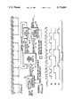
- FIG. 1 is a finite state transition diagram depicting the (2,18,2) code
- FIG. 2 is a block diagram of a data storage system embodying the invention
- FIG. 3 is a block diagram of the encoder
- FIG. 4 is a block diagram of the decoder
- FIG. 5 is a timing diagram of the control signals for the decoder.
- the (2,18,2) code is a run length limited code with traditional (d,k) constraints and the additional constraint that all run lengths of consecutive zeros are even.
- the (2,18,2) code can be described by the finite state transition diagram shown in FIG. 1.
- the capacity of the (2,18,2) constraint is sufficient to allow a rational code rate of 2/5.
- FIG. 2 illustrates a data storage system employing a (2,18,2) code and embodying the invention.
- a binary data stream from a source 10 is converted into a (2,18,2) code bit stream by an encoder 11.
- the code bit stream controls a writing means 12, such as a diode laser and associated electronics in an optical disk system or a magnetic recording head and associated electronics in a magnetic disk or tape system.
- the information, as encoded into (2,18,2) code by encoder 11, is written onto a medium 13, such as an optical or magnetic disk in the form of marks in the case of optical media or magnetic transitions in the case of magnetic media.
- the written marks or transitions are read back as an analog signal by a reading means 14, which may include a laser beam or magnetic reading head.
- This analog signal is converted back into a digital data stream representing the code data by a data detector and synchronizer 15 that is suitable for codes with even consecutive zeros and may be of the type described in the proceedings of the IEEE International Conference on Communications, Apr. 16-19, 1990, at pages 1729-1733.
- the data output of data detector and synchronizer 15 is decoded by a decoder 16 which converts the (2,18,2) code data back to the original binary representation.
- a finite state machine with only 25 states and four outgoing edges per state could be used to define the (2,18,2) encoding algorithm.
- This FSM is depicted in Table 1 (see Appendix). It describes the encoding rules used by encoder 11 and, because of its simplicity, allows practical implementation of a (2,18,2) code.
- Each edge of the FSM is represented by an entry in Table 1. Edges are selected during the encoding process according to the current state of the FSM and a two-bit input label. Each edge specifies a five-bit codeword and next state of the FSM. Encoded data is produced by tracing a path through the FSM. With each new set of two input bits, the correct edge is chosen from the current state and the codeword associated with the edge is output by encoder 11.
- the FSM in Table 1 was generated with only four rounds of state-splitting, which together with selective input edge assignment, enabled the design of a decoder having a window of only four codewords, an important feature of the invention. This limits error propagation upon decoding to eight bits.
- the two-bit input labels for each edge in Table 1 are chosen so as to allow unique decoding by a sliding block decoder.
- FIG. 3 illustrates the manner in which the FSM described in Table 1 can be implemented in hardware. Since the FSM has 25 states, at least five bits are required to represent a particular one of the states. The five state bits are identified as s1, . . . , s5 and the two input data bits as x1 and x2. These seven bits generate the codeword y1, . . . , y5 and the next state s1*, . . . , s5*.
- the clock ⁇ has a frequency that is five times higher than the bit rate of the input data stream and twice the bit rate of the code data. The other clocks, ⁇ /2, ⁇ /5 and ⁇ /10, are derived from ⁇ by frequency division by suitable means (not shown).
- serial input data 19 is converted to two parallel bits x1,x2 by a serial-to-parallel converter 20 which may be a serial-in, parallel-out shift register.
- the two parallel data bits x1 and x2 plus five state bits s1, . . . , s5 that identify the present state of encoder 11 are supplied to, and specify the address of a memory location in, a read only memory (ROM) 21.
- ROM 21 serves as a look-up table to generate the codeword bits y1, . . . , y5 and the bits s1*, . . . , s5* describing the next state of encoder 11.
- Register 22 holds the value of the current state of the FSM while the next state and codeword are generated.
- the codeword bits y1, . . . , y5 are converted into a serial data stream 23 by parallel-to-serial converter 24 which may be a parallel-in, serial-out shift register.
- parallel-to-serial converter 24 which may be a parallel-in, serial-out shift register.
- the encoding rules for the (2,18,2) encoder 11 can be converted into a truth table such as specified in Table 2 (see Appendix) by assigning a unique binary label to each state.
- Table 2 specifies the contents of ROM 21 for the case where states 1, . . . , 25 of the FSM have been assigned the binary values 00001, . . . , 11001; however, any other consistent assignment of binary values to FSM state labels may be used, if preferred.
- Table 2 can also be converted into logic equations using standard logic minimization techniques.
- ROM 21 can then be replaced by suitable combinational logic circuitry. For example, the logic expression for y1 would be
- decoder 16 for the (2,18,2) code uses a sliding window to convert five-bit codewords y1, . . . , y5 back to the correct two-bit sequences x1,x2, representing the recovered data.
- the input data stream for decoder 16 consists of concatenated five-bit codewords. In order to determine x1,x2, the current codeword and the three following codewords must be examined. Decoder 16 looks at a window of four five-bit codewords (a total of 20 bits) and produces the correct translation of the first one. When five new code bits are received, the window shifts forward one codeword and the process repeats.
- the decoder window is 20-bits wide
- This is possible since there are only eight different five-bit codewords output by encoder 11.
- These five-bit codewords y1, . . . , y5 are reassigned the smaller three-bit label z1,z2,z3 when received.
- These three-bit codewords are then used to form the needed window of four words, resulting in only 12 bits total. This reduction from 20 bits to 12 bits greatly reduces the size the circuitry used to determine recovered data bits.
- shift register 31 receives encoded data serially from data detector and synchronizer 15 and presents it in parallel to combinational codeword reassignment logic circuitry 32.
- Circuitry 32 receives five-bit codeword y1, . . . , y5 in parallel and converts it to a new three-bit representation z1, . . . , z3, as specified in Table 3.
- These three-bit codewords are made available in parallel to a twelve-bit address register 33.
- Address register 33 comprises three four-bit shift registers. Every fifth clock cycle a new codeword z1,z2,z3 is shifted into address register 33; with z1 going to the first shift register, z2 to the second, and z3 to the third.
- shift registers are four bits wide, so together they hold twelve bits of window information. This twelve-bit window addresses a look-up table in a ROM 34.
- the output of ROM 34 is the two bits x1,x2 decoded from the current codeword. These bits x1,x2 are then serialized through a register 35, multiplexor 36 and register 37 to provide recovered serial binary data in line 39.
- the control signals for decoder 16 are all generated from outputs QA,QB,QC from a counter 38 in response to clock pulses in line 40.
- Output QC is used to load new three-bit reassigned codewords into address register 33.
- Output QC also clocks x1,x2 pairs into register 35 where they can be held while serialized out through the combination of multiplexor 36 and register 37.
- Output QB is an input to the multiplexor which selects between x1 and x2, thus determining which data is being fed to register 37.
- Output QA serves as the output data clock and controls the clocking of data from the multiplexor into register 37.
- ROM 34 (shown in Table 4 of Appendix) are key to the operation of decoder 16.
- the look-up table was derived by considering all possible four codeword sequences generated by the encoder FSM, and choosing the correct x1,x2 for recovery in each case. There are a total of 100 edges (25 states ⁇ 4 edges per state) in encoder 11. In some cases, there are identical codeword sequences (also called edge sequences) that begin in different states. Each sequence begins with a different edge, but must decode to the same input if decoding is to be unique.
- the encoder FSM in Table 1 was designed with input assignments that allow these equivalent edge sequences to decode to the same x1,x2.
- the look-up truth table in Table 4 is written in terms of the three-bit codeword names or representations as reassigned in Table 3. The entries are written left to right with the oldest codeword (the one to be translated) at the left and the three following codewords (needed for the decoding window) to the right. When a new codeword is received, it shifts into the window from the right, as the oldest word (now decoded) shifts out to the left.
- Tables 2 and 4 were illustrated as implemented using ROMs 21 and 34, respectively, it will be understood that, if preferred, they may be implemented either in discrete logic circuitry or programmable logic arrays.
Landscapes
- Engineering & Computer Science (AREA)
- Theoretical Computer Science (AREA)
- Signal Processing (AREA)
- Signal Processing For Digital Recording And Reproducing (AREA)
Abstract
A rate 2/5 (2,18,2) code especially suitable for use with a resonant coil overwrite technique for magneto-optical recording. Serial binary input data is converted to serial binary code data that satisfies a (2,18,2) constraint and is reconverted to the serial binary input data. An encoder receives two sequential input bits and a five-bit state vector derived from an immediately preceding encoding operation, and generates a five-bit codeword and a new five-bit state vector based on the two input bits and five-bit state vector. A decoder converts the binary code data into five-bit codewords, converts each five-bit codeword sequentially into a reassigned three-bit codeword representation, then collects sets of four adjacent three-bit codeword representations. Each reassigned codeword representation is converted to a two-bit output corresponding to a then current set of said four three-bit codeword representations, and successive two-bit outputs are reconverted into the serial binary data.
Description
This is a continuation of copending application Ser. No. 07/605,288, filed on Oct. 29, 1990, now abandoned.
This invention relates to run length limited codes that allow high density recording for optical and/or magnetic storage media, and more particularly to a unique method of encoding and decoding a rate 2/5 even-consecutive-zero constraint (2,18,2) code that is especially suitable for use with a resonant coil direct overwrite technique for magneto-optical recording.
Run length limited (RLL) codes with an even-consecutive-zero constraint (i.e., an even number of "0" code bits between each "1" code bit) in addition to the usual d,k constraints, have heretofore been proposed and are designated (d,k,2).
For example, U.S. Pat. No. 4,928,187 describes a (2,8,2) code which means that it has run lengths of either 2, 4, 6 or 8 "0" code bits between each "1" code bit. This code is described as useful for a magnetic or optical medium data storage system. It has a rate 1/3, which means that for every data bit three code bits are required.
In the IEEE Transactions Magnetics, MAG-18, pp. 772-775 published in 1982, Funk described a similar rate 1/3 code satisfying the (2,8,2) constraint for magnetic recording.
In the Proceedings of the Optical Data Storage Topical Meeting (1989) reported in SPIE Vol. 1078 at pp. 265-270, it was reported that a rate 2/5 (2,18,2) code can be constructed using sliding block code techniques. However, no information was provided on how the code can be constructed or implemented. This (2,18,2) code requires five code bits for every two data bits and hence has a higher rate than the rate 1/3 codes. It is especially suitable for use with a resonant coil magneto-optic direct overwrite technique such as that described in U.S. Pat. No. 4,872,078, which discloses the only presently known field modulation overwrite technique compatible with parallel recording.
The (2,18,2) code has been found to be (a) superior to the (1,7), (2,7) and (2,8,2) codes when used for pulse width modulation (PWM) recording with either maximum slope or threshold detection channels; (b) superior to all other codes thus far modeled for optical partial response maximum likelihood (PRML) type channels, including (1,7) at linear densities above 45 kbpi; and (c) less susceptible to the effects of domain size variation. The main advantage of the (2,18,2) code in bit-by-bit detection is due to the wider detection window for a given user data density. The wide window is a consequence of the even-zero constraint which disallows every other clock period as a potential edge location.
There is a need for a practical method for encoding and decoding a rate 2/5 (2,18,2) code.
Serial binary input data is converted to serial binary code data that satisfies a (2,18,2) constraint and is reconverted to the serial binary input data. An encoder receives two sequential input bits and a five-bit state vector derived from an immediately preceding encoding operation, and generates a five-bit codeword and a new five-bit state vector based on said two input bits and five-bit state vector. A decoder converts the binary code data into five-bit codewords, converts each five-bit codeword sequentially into a reassigned three-bit codeword representation, then collects sets of four adjacent three-bit codeword representations. Each reassigned codeword representation is converted to a two-bit output corresponding to then current set of said four three-bit codeword representations, and successive two-bit outputs are reconverted into the serial binary data.
FIG. 1 is a finite state transition diagram depicting the (2,18,2) code;
FIG. 2 is a block diagram of a data storage system embodying the invention;
FIG. 3 is a block diagram of the encoder;
FIG. 4 is a block diagram of the decoder; and
FIG. 5 is a timing diagram of the control signals for the decoder.
The (2,18,2) code is a run length limited code with traditional (d,k) constraints and the additional constraint that all run lengths of consecutive zeros are even. The d=2 constraint serves to limit intersymbol interference and k=18 guarantees transitions close enough for timing recovery. The (2,18,2) code can be described by the finite state transition diagram shown in FIG. 1. The capacity of the (2,18,2) constraint is sufficient to allow a rational code rate of 2/5.
FIG. 2 illustrates a data storage system employing a (2,18,2) code and embodying the invention. A binary data stream from a source 10 is converted into a (2,18,2) code bit stream by an encoder 11. The code bit stream controls a writing means 12, such as a diode laser and associated electronics in an optical disk system or a magnetic recording head and associated electronics in a magnetic disk or tape system. The information, as encoded into (2,18,2) code by encoder 11, is written onto a medium 13, such as an optical or magnetic disk in the form of marks in the case of optical media or magnetic transitions in the case of magnetic media. The written marks or transitions are read back as an analog signal by a reading means 14, which may include a laser beam or magnetic reading head. This analog signal is converted back into a digital data stream representing the code data by a data detector and synchronizer 15 that is suitable for codes with even consecutive zeros and may be of the type described in the proceedings of the IEEE International Conference on Communications, Apr. 16-19, 1990, at pages 1729-1733. The data output of data detector and synchronizer 15 is decoded by a decoder 16 which converts the (2,18,2) code data back to the original binary representation.
An algorithm for sliding block codes is described in IEEE Transactions on Information Theory, published Jan. 1983 at pp. 5-22. This algorithm is described in more condensed form in IEEE Transactions on Magnetics, published Sep. 1985, at pp. 1348-1349. These articles describe state-splitting and state-merging.
According to a feature of the invention, applicants found that, by manipulation of the finite state transition diagram of FIG. 1 for the (2,18,2) code and making selective use of state-splitting methods, a finite state machine (FSM) with only 25 states and four outgoing edges per state could be used to define the (2,18,2) encoding algorithm. This FSM is depicted in Table 1 (see Appendix). It describes the encoding rules used by encoder 11 and, because of its simplicity, allows practical implementation of a (2,18,2) code.
Each edge of the FSM is represented by an entry in Table 1. Edges are selected during the encoding process according to the current state of the FSM and a two-bit input label. Each edge specifies a five-bit codeword and next state of the FSM. Encoded data is produced by tracing a path through the FSM. With each new set of two input bits, the correct edge is chosen from the current state and the codeword associated with the edge is output by encoder 11.
Thus, two bits of input data and the current state of the FSM serve to specify the five-bit codeword plus the next state of the FSM. Note that there are only 8 possible choices of codewords: 00000, 00001, 00010, 00100, 01000, 10000, 01001 and 10010.
The FSM in Table 1 was generated with only four rounds of state-splitting, which together with selective input edge assignment, enabled the design of a decoder having a window of only four codewords, an important feature of the invention. This limits error propagation upon decoding to eight bits. The two-bit input labels for each edge in Table 1 are chosen so as to allow unique decoding by a sliding block decoder.
FIG. 3 illustrates the manner in which the FSM described in Table 1 can be implemented in hardware. Since the FSM has 25 states, at least five bits are required to represent a particular one of the states. The five state bits are identified as s1, . . . , s5 and the two input data bits as x1 and x2. These seven bits generate the codeword y1, . . . , y5 and the next state s1*, . . . , s5*. The clock Φ has a frequency that is five times higher than the bit rate of the input data stream and twice the bit rate of the code data. The other clocks, Φ/2, Φ/5 and Φ/10, are derived from Φ by frequency division by suitable means (not shown).
In encoder 11, serial input data 19 is converted to two parallel bits x1,x2 by a serial-to-parallel converter 20 which may be a serial-in, parallel-out shift register. The two parallel data bits x1 and x2 plus five state bits s1, . . . , s5 that identify the present state of encoder 11 are supplied to, and specify the address of a memory location in, a read only memory (ROM) 21. ROM 21 serves as a look-up table to generate the codeword bits y1, . . . , y5 and the bits s1*, . . . , s5* describing the next state of encoder 11. Register 22 holds the value of the current state of the FSM while the next state and codeword are generated. The codeword bits y1, . . . , y5 are converted into a serial data stream 23 by parallel-to-serial converter 24 which may be a parallel-in, serial-out shift register. The encoding rules for the (2,18,2) encoder 11 can be converted into a truth table such as specified in Table 2 (see Appendix) by assigning a unique binary label to each state.
As illustrated, Table 2 specifies the contents of ROM 21 for the case where states 1, . . . , 25 of the FSM have been assigned the binary values 00001, . . . , 11001; however, any other consistent assignment of binary values to FSM state labels may be used, if preferred.
If desired, the truth table in Table 2 can also be converted into logic equations using standard logic minimization techniques. ROM 21 can then be replaced by suitable combinational logic circuitry. For example, the logic expression for y1 would be
y.sub.1 =x.sub.1 x.sub.2 s.sub.1 s.sub.4 s.sub.5 +s.sub.1 s.sub.2 s.sub.4 s.sub.5 +s.sub.1 s.sub.3 s.sub.4 +s.sub.1 s.sub.3 s.sub.4.
Referring now to FIG. 4, decoder 16 for the (2,18,2) code uses a sliding window to convert five-bit codewords y1, . . . , y5 back to the correct two-bit sequences x1,x2, representing the recovered data. The input data stream for decoder 16 consists of concatenated five-bit codewords. In order to determine x1,x2, the current codeword and the three following codewords must be examined. Decoder 16 looks at a window of four five-bit codewords (a total of 20 bits) and produces the correct translation of the first one. When five new code bits are received, the window shifts forward one codeword and the process repeats. Although the decoder window is 20-bits wide, the same information, according to an important feature of the invention, desirably can be conveyed in a 12-bit form by adopting the codeword reassignment shown in Table 3 (see Appendix) to produce the logic equation z1 =y1 +y2 ; z2 =y1 +y4 +y3 ; z3 =y5 +y3 +(y1 y4). This is possible since there are only eight different five-bit codewords output by encoder 11. These five-bit codewords y1, . . . , y5 are reassigned the smaller three-bit label z1,z2,z3 when received. These three-bit codewords are then used to form the needed window of four words, resulting in only 12 bits total. This reduction from 20 bits to 12 bits greatly reduces the size the circuitry used to determine recovered data bits.
More specifically, and as illustrated in FIG. 4, shift register 31 receives encoded data serially from data detector and synchronizer 15 and presents it in parallel to combinational codeword reassignment logic circuitry 32. Circuitry 32 receives five-bit codeword y1, . . . , y5 in parallel and converts it to a new three-bit representation z1, . . . , z3, as specified in Table 3. These three-bit codewords are made available in parallel to a twelve-bit address register 33. Address register 33 comprises three four-bit shift registers. Every fifth clock cycle a new codeword z1,z2,z3 is shifted into address register 33; with z1 going to the first shift register, z2 to the second, and z3 to the third. These shift registers are four bits wide, so together they hold twelve bits of window information. This twelve-bit window addresses a look-up table in a ROM 34. The output of ROM 34 is the two bits x1,x2 decoded from the current codeword. These bits x1,x2 are then serialized through a register 35, multiplexor 36 and register 37 to provide recovered serial binary data in line 39.
The control signals for decoder 16 are all generated from outputs QA,QB,QC from a counter 38 in response to clock pulses in line 40. Output QC is used to load new three-bit reassigned codewords into address register 33. Output QC also clocks x1,x2 pairs into register 35 where they can be held while serialized out through the combination of multiplexor 36 and register 37. Output QB is an input to the multiplexor which selects between x1 and x2, thus determining which data is being fed to register 37. Output QA serves as the output data clock and controls the clocking of data from the multiplexor into register 37.
The relationship between these control signals is shown in FIG. 5. The serial output issues with an asymmetrical clock having two output pulses for every five code clock pulses (as required for a rate 2/5 code). Counter 38 relies on the synchronization signal in line 41 to correctly align the decoder window. This synchronization signal is generated from a preamble that initiates the data stream.
The contents of ROM 34 (shown in Table 4 of Appendix) are key to the operation of decoder 16. The look-up table was derived by considering all possible four codeword sequences generated by the encoder FSM, and choosing the correct x1,x2 for recovery in each case. There are a total of 100 edges (25 states×4 edges per state) in encoder 11. In some cases, there are identical codeword sequences (also called edge sequences) that begin in different states. Each sequence begins with a different edge, but must decode to the same input if decoding is to be unique.
The encoder FSM in Table 1 was designed with input assignments that allow these equivalent edge sequences to decode to the same x1,x2. The look-up truth table in Table 4 is written in terms of the three-bit codeword names or representations as reassigned in Table 3. The entries are written left to right with the oldest codeword (the one to be translated) at the left and the three following codewords (needed for the decoding window) to the right. When a new codeword is received, it shifts into the window from the right, as the oldest word (now decoded) shifts out to the left.
While the truth tables of Tables 2 and 4 were illustrated as implemented using ROMs 21 and 34, respectively, it will be understood that, if preferred, they may be implemented either in discrete logic circuitry or programmable logic arrays.
While the invention has been shown and described with respect to preferred embodiments thereof, it will be understood by those skilled in the art that changes in form and detail may be made in these embodiments without departing from the scope and teaching of the invention. Accordingly, the apparatus and method herein disclosed are to be considered merely as illustrative, and the invention is to be limited only as specified in the claims.
              TABLE 1
______________________________________
Finite State Machine for (2,18,2) Encoder
        INPUT DATA
Current  00         01       10       11
State    *  **      *  **    *  **    *  **
______________________________________
01       04-00100   17-00100 18-00100 19-00100
02       06-00100   20-00100 21-00100 22-00100
03       01-00100   02-00100 03-00100 05-00100
04       13-00000   14-00000 15-00000 16-00000
05       08-00000   11-00000 23-00000 10-00000
06       04-00001   05-00001 06-00001 07-00001
07       01-00001   02-00001 03-00001 09-00000
08       13-01000   14-01000 15-01000 16-01000
09       04-00000   17-00000 18-00000 19-00000
10       20-00000   21-00000 06-00000 22-00000
11       08-01000   10-01000 11-01000 23-01000
12       01-00000   02-00000 03-00000 24-00000
13       13-00010   14-00010 15-00010 16-00010
14       09-00010   10-00010 11-00010 12-00010
15       01-01001   02-01001 03-01001 08-00010
16       04-01001   05-01001 06-01001 07-01001
17       04-10000   17-10000 18-10000 19-10000
18       06-10000   20-10000 21-10000 22-10000
19       01-10000   02-10000 03-10000 05-10000
20       09-10010   10-10010 11-10010 12-10010
21       13-10010   14-10010 15-10010 16-10010
22       01-00001   02-00001 03-00001 08-10010
23       01-00000   02-00000 03-00000 09-01000
24       08-00000   11-00000 23-00000 25-00000
25       20-00000   21-00000 18-00000 19-00000
______________________________________
 *next state
 **code word
              TABLE 2
______________________________________
Truth TABLE for Finite State Machine for (2,18,2) Decoder
______________________________________
00      00001         00100   00100
01      00001         10001   00100
10      00001         10010   00100
11      00001         10011   00100
00      00010         00110   00100
01      00010         10100   00100
10      00010         10101   00100
11      00010         10110   00100
00      00011         00001   00100
01      00011         00010   00100
10      00011         00011   00100
11      00011         00101   00100
00      00100         01101   00000
01      00100         01110   00000
10      00100         01111   00000
11      00100         10000   00000
00      00101         01000   00000
01      00101         01011   00000
10      00101         10111   00000
11      00101         01010   00000
00      00110         00100   00001
01      00110         00101   00001
10      00110         00110   00001
11      00110         00111   00001
00      00111         00001   00001
01      00111         00010   00001
10      00111         00011   00001
11      00111         01001   00000
00      01000         01101   01000
01      01000         01110   01000
10      01000         01111   01000
11      01000         10000   01000
00      01001         00100   00000
01      01001         10001   00000
10      01001         10010   00000
11      01001         10011   00000
00      01010         10100   00000
01      01010         10101   00000
10      01010         00110   00000
11      01010         10110   00000
00      01011         01000   01000
01      01011         01010   01000
10      01011         01011   01000
11      01011         10111   01000
00      01100         00001   00000
01      01100         00010   00000
10      01100         00011   00000
11      01100         11000   00000
00      01101         01101   00010
01      01101         01110   00010
10      01101         01111   00010
11      01101         10000   00010
00      01110         01001   00010
01      01110         01010   00010
10      01110         01011   00010
11      01110         01100   00010
00      01111         00001   01001
01      01111         00010   01001
10      01111         00011   01001
11      01111         01000   00010
00      10000         00100   01001
01      10000         00101   01001
10      10000         00110   01001
11      10000         00111   01001
00      10001         00100   10000
01      10001         10001   10000
10      10001         10010   10000
11      10001         10011   10000
00      10010         00110   10000
01      10010         10100   10000
10      10010         10101   10000
11      10010         10110   10000
00      10011         00001   10000
01      10011         00010   10000
10      10011         00011   10000
11      10011         00101   10000
00      10100         01001   10010
01      10100         01010   10010
10      10100         01011   10010
11      10100         01100   10010
00      10101         01101   10010
01      10101         01110   10010
10      10101         01111   10010
11      10101         10000   10010
00      10110         00001   00001
01      10110         00010   00001
10      10110         00011   00001
11      10110         01000   10010
00      10111         00001   00000
01      10111         00010   00000
10      10111         00011   00000
11      10111         01001   01000
00      11000         01000   00000
01      11000         01011   00000
10      11000         10111   00000
11      11000         11001   00000
00      11001         10100   00000
01      11001         10101   00000
10      11001         10010   00000
11      11001         10011   00000
______________________________________
              TABLE 3
______________________________________
Codeword Reassignment
Codeword     Reassigned Word
y.sub.1 y.sub.2 y.sub.3 y.sub.4 y.sub.5
             z.sub.1 z.sub.2 z.sub.3
______________________________________
0 0 0 0 0    0 0 0
0 0 0 0 1    0 0 1
0 0 0 1 0    0 1 0
0 0 1 0 0    0 1 1
0 1 0 0 0    1 0 0
0 1 0 0 1    1 0 1
1 0 0 0 0    1 1 0
1 0 0 1 0    1 1 1
Logic Equation
z.sub.1 = y.sub.1 + y.sub.2
z.sub.2 = y.sub.1 + y.sub.4 + y.sub.3
z.sub.3 = y.sub.5 + y.sub.3 + (y.sub.1 y.sub.4)
______________________________________
TABLE 4
______________________________________
(2,18,2) Look-up Truth TABLE for (2,18,2) Decoder
Input Output
Z.sub.1 Z.sub.2 Z.sub.3
Z.sub.1 Z.sub.2 Z.sub.3
Z.sub.1 Z.sub.2 Z.sub.3
Z.sub.1 Z.sub.2 Z.sub.3
X.sub.1 X.sub.2
______________________________________
[1] [2] [3] [4]
0 0 0 1 1 1 1 0 1 0 0 1 0 1
0 0 0 1 1 1 1 0 1 0 0 0 0 1
0 0 0 1 1 1 0 1 0 1 0 0 0 1
0 0 0 1 1 1 1 0 1 0 1 1 0 1
0 0 0 1 1 1 0 1 0 0 0 0 0 1
0 0 0 1 1 1 0 1 0 1 0 1 0 1
0 0 0 1 1 1 0 1 0 0 1 0 0 1
0 0 0 1 1 1 0 0 0 0 0 0 0 0
0 0 0 1 1 1 0 0 0 0 1 1 0 0
0 0 0 1 1 1 1 0 0 0 0 0 0 0
0 0 0 1 1 1 1 0 0 1 0 0 0 0
0 0 0 1 1 1 0 0 0 0 0 1 0 0
0 0 0 1 1 1 0 0 0 1 1 1 0 0
0 0 0 1 1 1 0 0 0 1 1 0 0 0
0 0 0 1 1 0 0 0 0 0 0 0 1 1
0 0 0 1 1 0 0 0 0 1 0 0 1 1
0 0 0 1 1 0 0 1 1 0 0 0 1 1
0 0 0 1 1 0 0 1 1 0 1 1 1 1
0 0 0 1 1 0 0 1 1 0 0 1 1 1
0 0 0 1 1 0 0 1 1 1 1 1 1 1
0 0 0 1 1 0 0 1 1 1 1 0 1 1
0 0 0 1 1 0 1 1 1 1 0 0 1 0
0 0 0 1 1 0 0 0 1 0 1 1 1 0
0 0 0 1 1 0 1 1 1 1 0 1 1 0
0 0 0 1 1 0 1 1 1 0 1 0 1 0
0 0 0 1 1 0 1 1 1 0 0 0 1 0
0 0 0 1 1 0 0 0 1 0 0 1 1 0
0 0 0 1 1 0 0 0 1 0 0 0 1 0
0 0 0 0 0 0 1 1 1 1 0 1 1 1
0 0 0 0 0 0 1 1 1 0 1 0 1 1
0 0 0 0 0 0 1 1 1 0 0 0 1 1
0 0 0 0 0 0 1 1 1 1 0 0 1 1
0 0 0 0 0 0 1 1 0 0 0 0 1 1
0 0 0 0 0 0 1 1 0 0 1 1 1 1
0 0 0 0 0 0 1 1 0 0 0 1 1 1
0 0 0 0 0 0 1 1 0 1 1 1 1 1
0 0 0 1 0 0 0 0 0 1 1 0 1 0
0 0 0 1 0 0 0 0 0 0 0 0 1 0
0 0 0 0 0 0 0 1 1 0 0 0 1 0
0 0 0 0 0 0 0 1 1 0 1 1 1 0
0 0 0 0 0 0 0 1 1 0 0 1 1 0
0 0 0 0 0 0 0 1 1 1 1 1 1 0
0 0 0 0 0 0 0 1 1 1 1 0 1 0
0 0 0 1 0 0 1 0 0 0 0 0 0 1
0 0 0 1 0 0 0 0 0 0 1 1 0 1
0 0 0 1 0 0 1 0 0 1 0 0 0 1
0 0 0 1 0 0 0 0 0 0 0 1 0 1
0 0 0 1 0 0 0 0 0 1 1 1 0 1
0 0 0 1 0 0 1 0 0 1 0 1 0 1
0 0 0 1 0 0 1 0 0 0 1 0 0 1
0 0 0 1 0 0 1 0 1 0 0 1 0 0
0 0 0 1 0 0 1 0 1 0 0 0 0 0
0 0 0 1 0 0 0 1 0 1 0 0 0 0
0 0 0 1 0 0 1 0 1 0 1 1 0 0
0 0 0 1 0 0 0 1 0 0 0 0 0 0
0 0 0 1 0 0 0 1 0 1 0 1 0 0
0 0 0 1 0 0 0 1 0 0 1 0 0 0
1 0 0 0 0 0 1 1 0 0 0 0 1 1
1 0 0 0 0 0 1 1 0 0 1 1 1 1
1 0 0 0 0 0 1 1 0 0 0 1 1 1
1 0 0 0 0 0 1 1 0 1 1 1 1 1
1 0 0 0 0 0 1 1 0 1 1 0 1 1
1 0 0 0 0 0 0 0 0 1 0 1 1 1
1 0 0 0 0 0 0 0 0 0 1 0 1 1
1 0 0 0 1 1 0 0 0 0 0 0 1 0
0 0 0 0 1 1 0 0 0 1 0 0 1 0
0 0 0 0 1 1 0 1 1 0 0 0 1 0
0 0 0 0 1 1 0 1 1 0 1 1 1 0
0 0 0 0 1 1 0 1 1 0 0 1 1 0
0 0 0 0 1 1 0 1 1 1 1 1 1 0
0 0 0 0 1 1 0 1 1 1 1 0 1 0
0 0 0 0 1 1 1 1 1 1 0 0 0 1
0 0 0 0 1 1 0 0 1 0 1 1 0 1
0 0 0 0 1 1 1 1 1 1 0 1 0 1
0 0 0 0 1 1 1 1 1 0 1 0 0 1
0 0 0 0 1 1 1 1 1 0 0 0 0 1
0 0 0 0 1 1 0 0 1 0 0 1 0 1
0 0 0 0 1 1 0 0 1 0 0 0 0 1
0 0 0 0 1 1 1 1 0 0 0 0 0 0
0 0 0 0 1 1 1 1 0 0 1 1 0 0
0 0 0 0 1 1 1 1 0 0 0 1 0 0
0 0 0 0 1 1 1 1 0 1 1 1 0 0
0 0 0 0 1 1 1 1 0 1 1 0 0 0
0 0 0 0 1 1 0 0 0 1 0 1 0 0
0 0 0 0 1 1 0 0 0 0 1 0 0 0
1 1 1 1 0 0 1 0 1 0 0 1 1 1
1 1 1 1 0 0 1 0 1 0 0 0 1 1
1 1 1 1 0 0 0 1 0 1 0 0 1 1
1 1 1 1 0 0 1 0 1 0 1 1 1 1
1 1 1 1 0 0 0 1 0 0 0 0 1 1
1 1 1 1 0 0 0 1 0 1 0 1 1 1
1 1 1 1 0 0 0 1 0 0 1 0 1 1
0 0 1 0 1 1 0 0 0 0 0 0 1 0
0 0 1 0 1 1 0 0 0 1 0 0 1 0
0 0 1 0 1 1 0 1 1 0 0 0 1 0
0 0 1 0 1 1 0 1 1 0 1 1 1 0
0 0 1 0 1 1 0 1 1 0 0 1 1 0
0 0 1 0 1 1 0 1 1 1 1 1 1 0
0 0 1 0 1 1 0 1 1 1 1 0 1 0
0 0 1 0 1 1 1 1 1 1 0 0 0 1
0 0 1 0 1 1 0 0 1 0 1 1 0 1
0 0 1 0 1 1 1 1 1 1 0 1 0 1
0 0 1 0 1 1 1 1 1 0 1 0 0 1
0 0 1 0 1 1 1 1 1 0 0 0 0 1
0 0 1 0 1 1 0 0 1 0 0 1 0 1
0 0 1 0 1 1 0 0 1 0 0 0 0 1
0 0 1 0 1 1 1 1 0 0 0 0 0 0
0 0 1 0 1 1 1 1 0 0 1 1 0 0
0 0 1 0 1 1 1 1 0 0 0 1 0 0
0 0 1 0 1 1 1 1 0 1 1 1 0 0
0 0 1 0 1 1 1 1 0 1 1 0 0 0
0 0 1 0 1 1 0 0 0 1 0 1 0 0
0 0 1 0 1 1 0 0 0 0 1 0 0 0
1 1 1 1 0 1 0 0 0 0 0 0 1 1
1 1 1 1 0 1 0 0 1 0 1 1 1 1
1 1 1 1 0 1 0 0 1 0 0 1 1 1
1 1 1 1 0 1 0 0 1 0 0 0 1 1
1 1 1 1 0 1 0 0 0 1 0 0 1 1
1 1 1 1 0 1 0 0 0 1 0 1 1 1
1 1 1 1 0 1 0 0 0 0 1 0 1 1
1 1 1 0 1 0 1 0 0 1 0 1 1 0
1 1 1 0 1 0 1 0 0 0 1 0 1 0
1 1 1 1 0 1 0 1 1 0 0 0 1 0
1 1 1 1 0 1 0 1 1 0 1 1 1 0
1 1 1 1 0 1 0 1 1 0 0 1 1 0
1 1 1 1 0 1 0 1 1 1 1 1 1 0
1 1 1 1 0 1 0 1 1 1 1 0 1 0
1 1 1 0 1 0 0 0 0 0 0 0 0 1
1 1 1 0 1 0 0 0 0 0 1 1 0 1
1 1 1 0 1 0 1 0 0 0 0 0 0 1
1 1 1 0 1 0 1 0 0 1 0 0 0 1
1 1 1 0 1 0 0 0 0 0 0 1 0 1
1 1 1 0 1 0 0 0 0 1 1 1 0 1
1 1 1 0 1 0 0 0 0 1 1 0 0 1
1 1 1 0 1 0 1 0 1 0 0 1 0 0
1 1 1 0 1 0 1 0 1 0 0 0 0 0
1 1 1 0 1 0 0 1 0 1 0 0 0 0
1 1 1 0 1 0 1 0 1 0 1 1 0 0
1 1 1 0 1 0 0 1 0 0 0 0 0 0
1 1 1 0 1 0 0 1 0 1 0 1 0 0
1 1 1 0 1 0 0 1 0 0 1 0 0 0
1 1 1 0 0 0 0 0 0 0 0 0 1 1
1 1 1 0 0 0 0 0 0 1 0 0 1 1
1 1 1 0 0 0 0 1 1 0 0 0 1 1
1 1 1 0 0 0 0 1 1 0 1 1 1 1
1 1 1 0 0 0 0 1 1 0 0 1 1 1
1 1 1 0 0 0 0 1 1 1 1 1 1 1
1 1 1 0 0 0 0 1 1 1 1 0 1 1
1 1 1 1 0 0 1 0 0 0 0 0 1 0
1 1 1 1 0 0 0 0 0 0 1 1 1 0
1 1 1 1 0 0 1 0 0 1 0 0 1 0
1 1 1 1 0 0 0 0 0 0 0 1 1 0
1 1 1 1 0 0 0 0 0 1 1 1 1 0
1 1 1 1 0 0 1 0 0 1 0 1 1 0
1 1 1 1 0 0 1 0 0 0 1 0 1 0
1 1 1 0 0 0 1 1 1 1 0 0 0 1
1 1 1 0 0 0 0 0 1 0 1 1 0 1
1 1 1 0 0 0 1 1 1 1 0 1 0 1
1 1 1 0 0 0 1 1 1 0 1 0 0 1
1 1 1 0 0 0 1 1 1 0 0 0 0 1
1 1 1 0 0 0 0 0 1 0 0 1 0 1
1 1 1 0 0 0 0 0 1 0 0 0 0 1
1 1 1 0 0 0 1 1 0 0 0 0 0 0
1 1 1 0 0 0 1 1 0 0 1 1 0 0
1 1 1 0 0 0 1 1 0 0 0 1 0 0
1 1 1 0 0 0 1 1 0 1 1 1 0 0
1 1 1 0 0 0 1 1 0 1 1 0 0 0
1 1 1 0 0 0 0 0 0 1 0 1 0 0
1 1 1 0 0 0 0 0 0 0 1 0 0 0
1 1 0 0 0 0 1 0 0 0 0 0 1 1
1 1 0 0 0 0 0 0 0 0 1 1 1 1
1 1 0 0 0 0 1 0 0 1 0 0 1 1
1 1 0 0 0 0 0 0 0 0 0 1 1 1
1 1 0 0 0 0 0 0 0 1 1 1 1 1
1 1 0 0 0 0 1 0 0 1 0 1 1 1
1 1 0 0 0 0 1 0 0 0 1 0 1 1
1 1 0 0 1 1 0 0 0 0 0 0 1 0
1 1 0 0 1 1 0 0 0 1 0 0 1 0
1 1 0 0 1 1 0 1 1 0 0 0 1 0
1 1 0 0 1 1 0 1 1 0 1 1 1 0
1 1 0 0 1 1 0 1 1 0 0 1 1 0
1 1 0 0 1 1 0 1 1 1 1 1 1 0
1 1 0 0 1 1 0 1 1 1 1 0 1 0
1 1 0 0 1 1 1 1 1 1 0 0 0 1
1 1 0 0 1 1 0 0 1 0 1 1 0 1
1 1 0 0 1 1 1 1 1 1 0 1 0 1
1 1 0 0 1 1 1 1 1 0 1 0 0 1
1 1 0 0 1 1 1 1 1 0 0 0 0 1
1 1 0 0 1 1 0 0 1 0 0 1 0 1
1 1 0 0 1 1 0 0 1 0 0 0 0 1
1 1 0 0 1 1 1 1 0 0 0 0 0 0
1 1 0 0 1 1 1 1 0 0 1 1 0 0
1 1 0 0 1 1 1 1 0 0 0 1 0 0
1 1 0 0 1 1 1 1 0 1 1 1 0 0
1 1 0 0 1 1 1 1 0 1 1 0 0 0
1 1 0 0 1 1 0 0 0 1 0 1 0 0
1 1 0 0 1 1 0 0 0 0 1 0 0 0
1 1 0 1 1 1 1 0 0 1 0 1 1 1
1 1 0 1 1 1 1 0 0 0 1 0 1 1
1 1 0 0 0 1 0 1 1 0 0 0 1 1
1 1 0 0 0 1 0 1 1 0 1 1 1 1
1 1 0 0 0 1 0 1 1 0 0 1 1 1
1 1 0 0 0 1 0 1 1 1 1 1 1 1
1 1 0 0 0 1 0 1 1 1 1 0 1 1
1 1 0 1 1 1 1 0 1 0 0 1 1 0
1 1 0 1 1 1 1 0 1 0 0 0 1 0
1 1 0 1 1 1 0 1 0 1 0 0 1 0
1 1 0 1 1 1 1 0 1 0 1 1 1 0
1 1 0 1 1 1 0 1 0 0 0 0 1 0
1 1 0 1 1 1 0 1 0 1 0 1 1 0
1 1 0 1 1 1 0 1 0 0 1 0 1 0
1 1 0 1 1 1 0 0 0 0 0 0 0 1
1 1 0 1 1 1 0 0 0 0 1 1 0 1
1 1 0 1 1 1 1 0 0 0 0 0 0 1
1 1 0 1 1 1 1 0 0 1 0 0 0 1
1 1 0 1 1 1 0 0 0 0 0 1 0 1
1 1 0 1 1 1 0 0 0 1 1 1 0 1
1 1 0 1 1 1 0 0 0 1 1 0 0 1
1 1 0 0 0 1 0 0 0 0 0 0 0 0
1 1 0 0 0 1 0 0 1 0 1 1 0 0
1 1 0 0 0 1 0 0 1 0 0 1 0 0
1 1 0 0 0 1 0 0 1 0 0 0 0 0
1 1 0 0 0 1 0 0 0 1 0 0 0 0
1 1 0 0 0 1 0 0 0 1 0 1 0 0
1 1 0 0 0 1 0 0 0 0 1 0 0 0
1 1 0 1 1 0 0 0 0 0 0 0 1 1
1 1 0 1 1 0 0 0 0 1 0 0 1 1
1 1 0 1 1 0 0 1 1 0 0 0 1 1
1 1 0 1 1 0 0 1 1 0 1 1 1 1
1 1 0 1 1 0 0 1 1 0 0 1 1 1
1 1 0 1 1 0 0 1 1 1 1 1 1 1
1 1 0 1 1 0 0 1 1 1 1 0 1 1
1 1 0 1 1 0 1 1 1 1 0 0 1 0
1 1 0 1 1 0 0 0 1 0 1 1 1 0
1 1 0 1 1 0 1 1 1 1 0 1 1 0
1 1 0 1 1 0 1 1 1 0 1 0 1 0
1 1 0 1 1 0 1 1 1 0 0 0 1 0
1 1 0 1 1 0 0 0 1 0 0 1 1 0
1 1 0 1 1 0 0 0 1 0 0 0 1 0
1 1 0 1 1 0 1 1 0 0 0 0 0 1
1 1 0 1 1 0 1 1 0 0 1 1 0 1
1 1 0 1 1 0 1 1 0 0 0 1 0 1
1 1 0 1 1 0 1 1 0 1 1 1 0 1
1 1 0 1 1 0 1 1 0 1 1 0 0 1
1 1 0 1 1 0 0 0 0 1 0 1 0 1
1 1 0 1 1 0 0 0 0 0 1 0 0 1
1 1 0 0 0 0 1 0 1 0 0 1 0 0
1 1 0 0 0 0 1 0 1 0 0 0 0 0
1 1 0 0 0 0 0 1 0 1 0 0 0 0
1 1 0 0 0 0 1 0 1 0 1 1 0 0
1 1 0 0 0 0 0 1 0 0 0 0 0 0
1 1 0 0 0 0 0 1 0 1 0 1 0 0
1 1 0 0 0 0 0 1 0 0 1 0 0 0
1 0 1 0 0 0 0 0 0 1 1 0 1 1
1 0 1 0 0 0 0 0 0 0 0 0 1 1
1 0 1 0 0 1 0 1 1 0 0 0 1 1
1 0 1 0 0 1 0 1 1 0 1 1 1 1
1 0 1 0 0 1 0 1 1 0 0 1 1 1
1 0 1 0 0 1 0 1 1 1 1 1 1 1
1 0 1 0 0 1 0 1 1 1 1 0 1 1
1 0 1 0 0 1 0 0 0 0 0 0 1 0
1 0 1 0 0 1 0 0 1 0 1 1 1 0
1 0 1 0 0 1 0 0 1 0 0 1 1 0
1 0 1 0 0 1 0 0 1 0 0 0 1 0
1 0 1 0 0 1 0 0 0 1 0 0 1 0
1 0 1 0 0 1 0 0 0 1 0 1 1 0
1 0 1 0 0 1 0 0 0 0 1 0 1 0
1 0 1 0 0 0 1 0 0 0 0 0 0 1
1 0 1 0 0 0 0 0 0 0 1 1 0 1
1 0 1 0 0 0 1 0 0 1 0 0 0 1
1 0 1 0 0 0 0 0 0 0 0 1 0 1
1 0 1 0 0 0 0 0 0 1 1 1 0 1
1 0 1 0 0 0 1 0 0 1 0 1 0 1
1 0 1 0 0 0 1 0 0 0 1 0 0 1
1 0 1 0 0 0 1 0 1 0 0 1 0 0
1 0 1 0 0 0 1 0 1 0 0 0 0 0
1 0 1 0 0 0 0 1 0 1 0 0 0 0
1 0 1 0 0 0 1 0 1 0 1 1 0 0
1 0 1 0 0 0 0 1 0 0 0 0 0 0
1 0 1 0 0 0 0 1 0 1 0 1 0 0
1 0 1 0 0 0 0 1 0 0 1 0 0 0
0 1 0 1 0 0 1 0 1 0 0 1 1 1
0 1 0 1 0 0 1 0 1 0 0 0 1 1
0 1 0 1 0 0 0 1 0 1 0 0 1 1
0 1 0 1 0 0 1 0 1 0 1 1 1 1
0 1 0 1 0 0 0 1 0 0 0 0 1 1
0 1 0 1 0 0 0 1 0 1 0 1 1 1
0 1 0 1 0 0 0 1 0 0 1 0 1 1
1 0 1 0 1 1 0 0 0 0 0 0 1 0
1 0 1 0 1 1 0 0 0 1 0 0 1 0
1 0 1 0 1 1 0 1 1 0 0 0 1 0
1 0 1 0 1 1 0 1 1 0 1 1 1 0
1 0 1 0 1 1 0 1 1 0 0 1 1 0
1 0 1 0 1 1 0 1 1 1 1 1 1 0
1 0 1 0 1 1 0 1 1 1 1 0 1 0
1 0 1 0 1 1 1 1 1 1 0 0 0 1
1 0 1 0 1 1 0 0 1 0 1 1 0 1
1 0 1 0 1 1 1 1 1 1 0 1 0 1
1 0 1 0 1 1 1 1 1 0 1 0 0 1
1 0 1 0 1 1 1 1 1 0 0 0 0 1
1 0 1 0 1 1 0 0 1 0 0 1 0 1
1 0 1 0 1 1 0 0 1 0 0 0 0 1
1 0 1 0 1 1 1 1 0 0 0 0 0 0
1 0 1 0 1 1 1 1 0 0 1 1 0 0
1 0 1 0 1 1 1 1 0 0 0 1 0 0
1 0 1 0 1 1 1 1 0 1 1 1 0 0
1 0 1 0 1 1 1 1 0 1 1 0 0 0
1 0 1 0 1 1 0 0 0 1 0 1 0 0
1 0 1 0 1 1 0 0 0 0 1 0 0 0
0 1 0 0 0 0 0 0 0 0 0 0 1 1
0 1 0 0 0 0 0 0 0 1 0 0 1 1
0 1 0 0 0 0 0 1 1 0 0 0 1 1
0 1 0 0 0 0 0 1 1 0 1 1 1 1
0 1 0 0 0 0 0 1 1 0 0 1 1 1
0 1 0 0 0 0 0 1 1 1 1 1 1 1
0 1 0 0 0 0 0 1 1 1 1 0 1 1
0 1 0 1 0 0 1 0 0 0 0 0 1 0
0 1 0 1 0 0 0 0 0 0 1 1 1 0
0 1 0 1 0 0 1 0 0 1 0 0 1 0
0 1 0 1 0 0 0 0 0 0 0 1 1 0
0 1 0 1 0 0 0 0 0 1 1 1 1 0
0 1 0 1 0 0 1 0 0 1 0 1 1 0
0 1 0 1 0 0 1 0 0 0 1 0 1 0
0 1 0 0 0 0 1 1 1 1 0 0 0 1
0 1 0 0 0 0 0 0 1 0 1 1 0 1
0 1 0 0 0 0 1 1 1 1 0 1 0 1
0 1 0 0 0 0 1 1 1 0 1 0 0 1
0 1 0 0 0 0 1 1 1 0 0 0 0 1
0 1 0 0 0 0 0 0 1 0 0 1 0 1
0 1 0 0 0 0 0 0 1 0 0 0 0 1
0 1 0 0 0 0 1 1 0 0 0 0 0 0
0 1 0 0 0 0 1 1 0 0 1 1 0 0
0 1 0 0 0 0 1 1 0 0 0 1 0 0
0 1 0 0 0 0 1 1 0 1 1 1 0 0
0 1 0 0 0 0 1 1 0 1 1 0 0 0
0 1 0 0 0 0 0 0 0 1 0 1 0 0
0 1 0 0 0 0 0 0 0 0 1 0 0 0
0 1 0 1 0 1 0 0 0 0 0 0 1 1
0 1 0 1 0 1 0 0 1 0 1 1 1 1
0 1 0 1 0 1 0 0 1 0 0 1 1 1
0 1 0 1 0 1 0 0 1 0 0 0 1 1
0 1 0 1 0 1 0 0 0 1 0 0 1 1
0 1 0 1 0 1 0 0 0 1 0 1 1 1
0 1 0 1 0 1 0 0 0 0 1 0 1 1
0 1 0 0 1 0 1 0 0 1 0 1 1 0
0 1 0 0 1 0 1 0 0 0 1 0 1 0
0 1 0 1 0 1 0 1 1 0 0 0 1 0
0 1 0 1 0 1 0 1 1 0 1 1 1 0
0 1 0 1 0 1 0 1 1 0 0 1 1 0
0 1 0 1 0 1 0 1 1 1 1 1 1 0
0 1 0 1 0 1 0 1 1 1 1 0 1 0
0 1 0 0 1 0 0 0 0 0 0 0 0 1
0 1 0 0 1 0 0 0 0 0 1 1 0 1
0 1 0 0 1 0 1 0 0 0 0 0 0 1
0 1 0 0 1 0 1 0 0 1 0 0 0 1
0 1 0 0 1 0 0 0 0 0 0 1 0 1
0 1 0 0 1 0 0 0 0 1 1 1 0 1
0 1 0 0 1 0 0 0 0 1 1 0 0 1
0 1 0 0 1 0 1 0 1 0 0 1 0 0
0 1 0 0 1 0 1 0 1 0 0 0 0 0
0 1 0 0 1 0 0 1 0 1 0 0 0 0
0 1 0 0 1 0 1 0 1 0 1 1 0 0
0 1 0 0 1 0 0 1 0 0 0 0 0 0
0 1 0 0 1 0 0 1 0 1 0 1 0 0
0 1 0 0 1 0 0 1 0 0 1 0 0 0
0 0 0 0 0 0 0 0 0 1 1 1 1 1
0 0 0 0 0 0 0 0 0 1 1 0 1 1
0 0 0 0 0 0 1 0 0 0 0 0 1 1
0 0 0 0 0 0 0 0 0 0 1 1 1 1
0 0 0 0 0 0 1 0 0 1 0 0 1 1
0 0 0 0 0 0 1 0 0 1 0 1 1 1
0 0 0 0 0 0 1 0 0 0 1 0 1 1
1 0 0 1 0 0 0 0 0 1 1 0 1 1
1 0 0 1 0 0 0 0 0 0 0 0 1 1
1 0 0 0 0 0 0 1 1 0 0 0 1 1
1 0 0 0 0 0 0 1 1 0 1 1 1 1
1 0 0 0 0 0 0 1 1 0 0 1 1 1
1 0 0 0 0 0 0 1 1 1 1 1 1 1
1 0 0 0 0 0 0 1 1 1 1 0 1 1
1 0 0 1 0 0 1 0 0 0 0 0 1 0
1 0 0 1 0 0 0 0 0 0 1 1 1 0
1 0 0 1 0 0 1 0 0 1 0 0 1 0
1 0 0 1 0 0 0 0 0 0 0 1 1 0
1 0 0 1 0 0 0 0 0 1 1 1 1 0
1 0 0 1 0 0 1 0 0 1 0 1 1 0
1 0 0 1 0 0 1 0 0 0 1 0 1 0
1 0 0 0 0 0 1 1 1 1 0 0 0 1
1 0 0 0 0 0 0 0 1 0 1 1 0 1
1 0 0 0 0 0 1 1 1 1 0 1 0 1
1 0 0 0 0 0 1 1 1 0 1 0 0 1
1 0 0 0 0 0 1 1 1 0 0 0 0 1
1 0 0 0 0 0 0 0 1 0 0 1 0 1
1 0 0 0 0 0 0 0 1 0 0 0 0 1
1 0 0 1 0 0 1 0 1 0 0 1 0 0
1 0 0 1 0 0 1 0 1 0 0 0 0 0
1 0 0 1 0 0 0 1 0 1 0 0 0 0
1 0 0 1 0 0 1 0 1 0 1 1 0 0
1 0 0 1 0 0 0 1 0 0 0 0 0 0
1 0 0 1 0 0 0 1 0 1 0 1 0 0
1 0 0 1 0 0 0 1 0 0 1 0 0 0
0 0 0 1 1 1 1 0 0 1 0 1 1 1
0 0 0 1 1 1 1 0 0 0 1 0 1 1
0 0 0 0 0 1 0 1 1 0 0 0 1 1
0 0 0 0 0 1 0 1 1 0 1 1 1 1
0 0 0 0 0 1 0 1 1 0 0 1 1 1
0 0 0 0 0 1 0 1 1 1 1 1 1 1
0 0 0 0 0 1 0 1 1 1 1 0 1 1
0 0 0 0 0 1 0 0 0 0 0 0 1 0
0 0 0 0 0 1 0 0 1 0 1 1 1 0
0 0 0 0 0 1 0 0 1 0 0 1 1 0
0 0 0 0 0 1 0 0 1 0 0 0 1 0
0 0 0 0 0 1 0 0 0 1 0 0 1 0
0 0 0 0 0 1 0 0 0 1 0 1 1 0
0 0 0 0 0 1 0 0 0 0 1 0 1 0
0 0 0 1 1 0 1 1 0 0 0 0 0 1
0 0 0 1 1 0 1 1 0 0 1 1 0 1
0 0 0 1 1 0 1 1 0 0 0 1 0 1
0 0 0 1 1 0 1 1 0 1 1 1 0 1
0 0 0 1 1 0 1 1 0 1 1 0 0 1
0 0 0 1 1 0 0 0 0 1 0 1 0 1
0 0 0 1 1 0 0 0 0 0 1 0 0 1
0 0 0 0 0 0 1 0 1 0 0 1 0 0
0 0 0 0 0 0 1 0 1 0 0 0 0 0
0 0 0 0 0 0 0 1 0 1 0 0 0 0
0 0 0 0 0 0 1 0 1 0 1 1 0 0
0 0 0 0 0 0 0 1 0 0 0 0 0 0
0 0 0 0 0 0 0 1 0 1 0 1 0 0
0 0 0 0 0 0 0 1 0 0 1 0 0 0
1 0 0 1 0 1 0 0 0 0 0 0 1 1
1 0 0 1 0 1 0 0 1 0 1 1 1 1
1 0 0 1 0 1 0 0 1 0 0 1 1 1
1 0 0 1 0 1 0 0 1 0 0 0 1 1
1 0 0 1 0 1 0 0 0 1 0 0 1 1
1 0 0 1 0 1 0 0 0 1 0 1 1 1
1 0 0 1 0 1 0 0 0 0 1 0 1 1
1 0 0 0 1 0 1 0 0 1 0 1 1 0
1 0 0 0 1 0 1 0 0 0 1 0 1 0
1 0 0 1 0 1 0 1 1 0 0 0 1 0
1 0 0 1 0 1 0 1 1 0 1 1 1 0
1 0 0 1 0 1 0 1 1 0 0 1 1 0
1 0 0 1 0 1 0 1 1 1 1 1 1 0
1 0 0 1 0 1 0 1 1 1 1 0 1 0
1 0 0 0 1 0 0 0 0 0 0 0 0 1
1 0 0 0 1 0 0 0 0 0 1 1 0 1
1 0 0 0 1 0 1 0 0 0 0 0 0 1
1 0 0 0 1 0 1 0 0 1 0 0 0 1
1 0 0 0 1 0 0 0 0 0 0 1 0 1
1 0 0 0 1 0 0 0 0 1 1 1 0 1
1 0 0 0 1 0 0 0 0 1 1 0 0 1
1 0 0 0 1 0 1 0 1 0 0 1 0 0
1 0 0 0 1 0 1 0 1 0 0 0 0 0
1 0 0 0 1 0 0 1 0 1 0 0 0 0
1 0 0 0 1 0 1 0 1 0 1 1 0 0
1 0 0 0 1 0 0 1 0 0 0 0 0 0
1 0 0 0 1 0 0 1 0 1 0 1 0 0
1 0 0 0 1 0 0 1 0 0 1 0 0 0
0 0 0 0 0 0 1 1 0 1 1 0 1 1
0 0 0 0 0 0 0 0 0 1 0 1 1 1
0 0 0 0 0 0 0 0 0 0 1 0 1 1
0 0 1 0 0 0 0 0 0 1 1 0 1 1
0 0 1 0 0 0 0 0 0 0 0 0 1 1
0 0 1 0 0 1 0 1 1 0 0 0 1 1
0 0 1 0 0 1 0 1 1 0 1 1 1 1
0 0 1 0 0 1 0 1 1 0 0 1 1 1
0 0 1 0 0 1 0 1 1 1 1 1 1 1
0 0 1 0 0 1 0 1 1 1 1 0 1 1
0 0 1 0 0 1 0 0 0 0 0 0 1 0
0 0 1 0 0 1 0 0 1 0 1 1 1 0
0 0 1 0 0 1 0 0 1 0 0 1 1 0
0 0 1 0 0 1 0 0 1 0 0 0 1 0
0 0 1 0 0 1 0 0 0 1 0 0 1 0
0 0 1 0 0 1 0 0 0 1 0 1 1 0
0 0 1 0 0 1 0 0 0 0 1 0 1 0
0 0 1 0 0 0 1 0 0 0 0 0 0 1
0 0 1 0 0 0 0 0 0 0 1 1 0 1
0 0 1 0 0 0 1 0 0 1 0 0 0 1
0 0 1 0 0 0 0 0 0 0 0 1 0 1
0 0 1 0 0 0 0 0 0 1 1 1 0 1
0 0 1 0 0 0 1 0 0 1 0 1 0 1
0 0 1 0 0 0 1 0 0 0 1 0 0 1
0 0 1 0 0 0 1 0 1 0 0 1 0 0
0 0 1 0 0 0 1 0 1 0 0 0 0 0
0 0 1 0 0 0 0 1 0 1 0 0 0 0
0 0 1 0 0 0 1 0 1 0 1 1 0 0
0 0 1 0 0 0 0 1 0 0 0 0 0 0
0 0 1 0 0 0 0 1 0 1 0 1 0 0
0 0 1 0 0 0 0 1 0 0 1 0 0 0
0 0 0 0 0 0 0 0 1 0 1 1 1 1
0 0 0 0 0 0 0 0 1 0 0 1 1 1
0 0 0 0 0 0 0 0 1 0 0 0 1 1
0 0 0 1 0 1 0 0 0 0 0 0 1 1
0 0 0 1 0 1 0 0 1 0 1 1 1 1
0 0 0 1 0 1 0 0 1 0 0 1 1 1
0 0 0 1 0 1 0 0 1 0 0 0 1 1
0 0 0 1 0 1 0 0 0 1 0 0 1 1
0 0 0 1 0 1 0 0 0 1 0 1 1 1
0 0 0 1 0 1 0 0 0 0 1 0 1 1
0 0 0 0 1 0 1 0 0 1 0 1 1 0
0 0 0 0 1 0 1 0 0 0 1 0 1 0
0 0 0 1 0 1 0 1 1 0 0 0 1 0
0 0 0 1 0 1 0 1 1 0 1 1 1 0
0 0 0 1 0 1 0 1 1 0 0 1 1 0
0 0 0 1 0 1 0 1 1 1 1 1 1 0
0 0 0 1 0 1 0 1 1 1 1 0 1 0
0 0 0 0 1 0 0 0 0 0 0 0 0 1
0 0 0 0 1 0 0 0 0 0 1 1 0 1
0 0 0 0 1 0 1 0 0 0 0 0 0 1
0 0 0 0 1 0 1 0 0 1 0 0 0 1
0 0 0 0 1 0 0 0 0 0 0 1 0 1
0 0 0 0 1 0 0 0 0 1 1 1 0 1
0 0 0 0 1 0 0 0 0 1 1 0 0 1
0 0 0 0 1 0 1 0 1 0 0 1 0 0
0 0 0 0 1 0 1 0 1 0 0 0 0 0
0 0 0 0 1 0 0 1 0 1 0 0 0 0
0 0 0 0 1 0 1 0 1 0 1 1 0 0
0 0 0 0 1 0 0 1 0 0 0 0 0 0
0 0 0 0 1 0 0 1 0 1 0 1 0 0
0 0 0 0 1 0 0 1 0 0 1 0 0 0
0 1 1 0 0 0 1 0 0 0 0 0 1 1
0 1 1 0 0 0 0 0 0 0 1 1 1 1
0 1 1 0 0 0 1 0 0 1 0 0 1 1
0 1 1 0 0 0 0 0 0 0 0 1 1 1
0 1 1 0 0 0 0 0 0 1 1 1 1 1
0 1 1 0 0 0 1 0 0 1 0 1 1 1
0 1 1 0 0 0 1 0 0 0 1 0 1 1
0 1 1 0 1 1 0 0 0 0 0 0 1 0
0 1 1 0 1 1 0 0 0 1 0 0 1 0
0 1 1 0 1 1 0 1 1 0 0 0 1 0
0 1 1 0 1 1 0 1 1 0 1 1 1 0
0 1 1 0 1 1 0 1 1 0 0 1 1 0
0 1 1 0 1 1 0 1 1 1 1 1 1 0
0 1 1 0 1 1 0 1 1 1 1 0 1 0
0 1 1 0 1 1 1 1 1 1 0 0 0 1
0 1 1 0 1 1 0 0 1 0 1 1 0 1
0 1 1 0 1 1 1 1 1 1 0 1 0 1
0 1 1 0 1 1 1 1 1 0 1 0 0 1
0 1 1 0 1 1 1 1 1 0 0 0 0 1
0 1 1 0 1 1 0 0 1 0 0 1 0 1
0 1 1 0 1 1 0 0 1 0 0 0 0 1
0 1 1 0 1 1 1 1 0 0 0 0 0 0
0 1 1 0 1 1 1 1 0 0 1 1 0 0
0 1 1 0 1 1 1 1 0 0 0 1 0 0
0 1 1 0 1 1 1 1 0 1 1 1 0 0
0 1 1 0 1 1 1 1 0 1 1 0 0 0
0 1 1 0 1 1 0 0 0 1 0 1 0 0
0 1 1 0 1 1 0 0 0 0 1 0 0 0
0 1 1 1 1 1 1 0 0 1 0 1 1 1
0 1 1 1 1 1 1 0 0 0 1 0 1 1
0 1 1 0 0 1 0 1 1 0 0 0 1 1
0 1 1 0 0 1 0 1 1 0 1 1 1 1
0 1 1 0 0 1 0 1 1 0 0 1 1 1
0 1 1 0 0 1 0 1 1 1 1 1 1 1
0 1 1 0 0 1 0 1 1 1 1 0 1 1
0 1 1 1 1 1 1 0 1 0 0 1 1 0
0 1 1 1 1 1 1 0 1 0 0 0 1 0
0 1 1 1 1 1 0 1 0 1 0 0 1 0
0 1 1 1 1 1 1 0 1 0 1 1 1 0
0 1 1 1 1 1 0 1 0 0 0 0 1 0
0 1 1 1 1 1 0 1 0 1 0 1 1 0
0 1 1 1 1 1 0 1 0 0 1 0 1 0
0 1 1 1 1 1 0 0 0 0 0 0 0 1
0 1 1 1 1 1 0 0 0 0 1 1 0 1
0 1 1 1 1 1 1 0 0 0 0 0 0 1
0 1 1 1 1 1 1 0 0 1 0 0 0 1
0 1 1 1 1 1 0 0 0 0 0 1 0 1
0 1 1 1 1 1 0 0 0 1 1 1 0 1
0 1 1 1 1 1 0 0 0 1 1 0 0 1
0 1 1 0 0 1 0 0 0 0 0 0 0 0
0 1 1 0 0 1 0 0 1 0 1 1 0 0
0 1 1 0 0 1 0 0 1 0 0 1 0 0
0 1 1 0 0 1 0 0 1 0 0 0 0 0
0 1 1 0 0 1 0 0 0 1 0 0 0 0
0 1 1 0 0 1 0 0 0 1 0 1 0 0
0 1 1 0 0 1 0 0 0 0 1 0 0 0
0 1 1 1 1 0 0 0 0 0 0 0 1 1
0 1 1 1 1 0 0 0 0 1 0 0 1 1
0 1 1 1 1 0 0 1 1 0 0 0 1 1
0 1 1 1 1 0 0 1 1 0 1 1 1 1
0 1 1 1 1 0 0 1 1 0 0 1 1 1
0 1 1 1 1 0 0 1 1 1 1 1 1 1
0 1 1 1 1 0 0 1 1 1 1 0 1 1
0 1 1 1 1 0 1 1 1 1 0 0 1 0
0 1 1 1 1 0 0 0 1 0 1 1 1 0
0 1 1 1 1 0 1 1 1 1 0 1 1 0
0 1 1 1 1 0 1 1 1 0 1 0 1 0
0 1 1 1 1 0 1 1 1 0 0 0 1 0
0 1 1 1 1 0 0 0 1 0 0 1 1 0
0 1 1 1 1 0 0 0 1 0 0 0 1 0
0 1 1 1 1 0 1 1 0 0 0 0 0 1
0 1 1 1 1 0 1 1 0 0 1 1 0 1
0 1 1 1 1 0 1 1 0 0 0 1 0 1
0 1 1 1 1 0 1 1 0 1 1 1 0 1
0 1 1 1 1 0 1 1 0 1 1 0 0 1
0 1 1 1 1 0 0 0 0 1 0 1 0 1
0 1 1 1 1 0 0 0 0 0 1 0 0 1
0 1 1 0 0 0 1 0 1 0 0 1 0 0
0 1 1 0 0 0 1 0 1 0 0 0 0 0
0 1 1 0 0 0 0 1 0 1 0 0 0 0
0 1 1 0 0 0 1 0 1 0 1 1 0 0
0 1 1 0 0 0 0 1 0 0 0 0 0 0
0 1 1 0 0 0 0 1 0 1 0 1 0 0
0 1 1 0 0 0 0 1 0 0 1 0 0 0
______________________________________
Claims (7)
1. A data storage system in which data is written on and read from a data storage medium, comprising:
an encoder that receives digital electrical signals representing serial binary input data and comprises:
(i) a serial-to-parallel converter that converts two sequentially chosen bits of binary input data into two parallel bits;
(ii) a register for holding a five-bit current-state denoting vector of the encoder; and
(iii) a read only memory lookup table that, from an address specified by said two parallel bits and five-bit current-state-denoting vector, generates a five-bit next state vector that is supplied to and updates the register and also generates a five-bit codeword chosen from one of the following eight possible codewords: 00000, 00001, 00010, 00100, 01000, 10000, 10010, 01001 for encoding the binary input data into a (2, 18, 2) code;
(iv) a five-bit parallel-to serial converter for converting the five-bit codeword into electrical signals as a string of serial (2, 18, 2) binary encoded data; and
a transducer for writing the serial (2, 18, 2) binary encoded data onto the medium.
2. The system of claim 1, characterized in that the lookup table constitutes a finite state machine that has the following 25 states and paths between states for converting the binary input data into the string of serial (2, 18, 2) binary encoded data, the two sequentially chosen input bits being 00, 01, 10 or 11, and the next state and five-bit codeword being as denoted by hyphenated sequences below:
______________________________________
Current   INPUT DATA
State    00         01       10       11
______________________________________
01       04-00100   17-00100 18-00100 19-00100
02       06-00100   20-00100 21-00100 22-00100
03       01-00100   02-00100 03-00100 05-00100
04       13-00000   14-00000 15-00000 16-00000
05       08-00000   11-00000 23-00000 10-00000
06       04-00001   05-00001 06-00001 07-00001
07       01-00001   02-00001 03-00001 09-00000
08       13-01000   14-01000 15-01000 16-01000
09       04-00000   17-00000 18-00000 19-00000
10       20-00000   21-00000 06-00000 22-00000
11       08-01000   10-01000 11-01000 23-01000
12       01-00000   02-00000 03-00000 24-00000
13       13-00010   14-00010 15-00010 16-00010
14       09-00010   10-00010 11-00010 12-00010
15       01-01001   02-01001 03-01001 08-00010
16       04-01001   05-01001 06-01001 07-01001
17       04-10000   17-10000 18-10000 19-10000
18       06-10000   20-10000 21-10000 22-10000
19       01-10000   02-10000 03-10000 05-10000
20       09-10010   10-10010 11-10010 12-10010
21       13-10010   14-10010 15-10010 16-10010
22       01-00001   02-00001 03-00001 08-10010
23       01-00000   02-00000 03-00000 09-01000
24       08-00000   11-00000 23-00000 25-00000
25       20-00000   21-00000 18-00000 19-00000
______________________________________
3. The system of claim 1, wherein the transducer comprises a diode laser and the data storage system is an optical disk system.
4. The system of claim 1, wherein the transducer comprises a magnetic recording head and the data storage system is a magnetic recording system.
5. The system of claim 1, including
a sliding block decoder that decodes the string of serial (2, 18, 2) binary encoded data read from the medium into the serial binary input data, and comprises:
(i) a first shift register for converting the string of (2, 18, 2) serial binary encoded data into four five-bit codewords;
(ii) codeword reassignment logic circuitry for converting each five-bit codeword into a reassigned three-bit codeword representation;
(iii) an address register means comprising three four-bit shift registers for collecting sets of four adjacent three-bit codeword representations;
(iv) a read only memory look up table for converting each reassigned three-bit codeword representation to a two-bit output corresponding to a then current set of four three-bit codeword representations; and
(v) means including a second register, a multiplexor and a third register connected in series for converting successive two-bit outputs into the serial binary data.
6. A sliding block decoder for decoding into serial binary data a string of serial rate m/n code data read from a data recording medium, said apparatus comprising:
a first shaft register for converting the serial string to j n-bit codewords;
codeword reassignment logic circuitry for converting each n-bit codeword into a reassigned k-bit codeword representation, where k<n;
address register means comprising k j-bit shift registers for collecting sets of j adjacent k-bit codeword representations;
a read only memory look up table for converting each reassigned k-bit codeword representation to an m-bit output corresponding to a then current set of j k-bit codeword representations; and
means including a second register, a multiplexor and a third register connected in series for converting successive m-bit outputs into the serial binary data.
7. The decoder of claim 6, wherein m=2, k=3, j=4 and n=5 for decoding a rate 2/5 (2, 18, 2) run length limited code.
Priority Applications (1)
| Application Number | Priority Date | Filing Date | Title |
|---|---|---|---|
| US07/855,139 US5173694A (en) | 1990-10-29 | 1992-03-19 | Binary data encoding and decoding using a rate 2/5 (2,18,2) code |
Applications Claiming Priority (2)
| Application Number | Priority Date | Filing Date | Title |
|---|---|---|---|
| US60528890A | 1990-10-29 | 1990-10-29 | |
| US07/855,139 US5173694A (en) | 1990-10-29 | 1992-03-19 | Binary data encoding and decoding using a rate 2/5 (2,18,2) code |
Related Parent Applications (1)
| Application Number | Title | Priority Date | Filing Date |
|---|---|---|---|
| US60528890A Continuation | 1990-10-29 | 1990-10-29 |
Publications (1)
| Publication Number | Publication Date |
|---|---|
| US5173694A true US5173694A (en) | 1992-12-22 |
Family
ID=27084909
Family Applications (1)
| Application Number | Title | Priority Date | Filing Date |
|---|---|---|---|
| US07/855,139 Expired - Fee Related US5173694A (en) | 1990-10-29 | 1992-03-19 | Binary data encoding and decoding using a rate 2/5 (2,18,2) code |
Country Status (1)
| Country | Link |
|---|---|
| US (1) | US5173694A (en) |
Cited By (34)
| Publication number | Priority date | Publication date | Assignee | Title |
|---|---|---|---|---|
| US5349350A (en) * | 1991-10-31 | 1994-09-20 | Integral Peripherals, Inc. | Run length limited encoding/decoding system for low power disk drives |
| US5400023A (en) * | 1992-03-10 | 1995-03-21 | Sony Corporation | Modulating method and demodulating method as well as modulating apparatus and demodulating apparatus |
| US5422641A (en) * | 1991-12-09 | 1995-06-06 | Matsushita Electric Industrial Co., Ltd. | Digital modulator and demodulator circuit |
| US5444542A (en) * | 1991-04-23 | 1995-08-22 | Canon Kabushiki Kaisha | Image processing apparatus and method |
| US5528236A (en) * | 1993-03-22 | 1996-06-18 | Sony Corporation | Modulating method, demodulating method, modulating apparatus, and demodulating apparatus |
| US5535187A (en) * | 1993-12-15 | 1996-07-09 | Intenational Business Machines Corporation | High capacity run-length-limited coding system employing asymmetric and even-spaced codes |
| US5537422A (en) * | 1992-06-30 | 1996-07-16 | Sony Corporation | Synchronization signal detector, synchronization signal detecting method and demodulator |
| US5537382A (en) * | 1994-11-22 | 1996-07-16 | Optex Corporation | Partial response coding for a multi-level optical recording channel |
| US5572207A (en) * | 1994-09-23 | 1996-11-05 | International Business Machines Corporation | Method and apparatus for numeric-to-string conversion |
| US5657014A (en) * | 1995-05-12 | 1997-08-12 | Optex Corporation | M=7 (3,7) runlength limited code for multi-level data |
| US5659311A (en) * | 1995-05-12 | 1997-08-19 | Optex Corporation | M=6 (2,4) runlength limited code for multi-level data |
| US5659310A (en) * | 1995-05-12 | 1997-08-19 | Optex Corporation | M=5 (0,2) runlength limited code for multi-level data |
| US5663723A (en) * | 1995-05-12 | 1997-09-02 | Optex Corporation | M=7 (1,3) runlength limited code for multi-level data |
| US5663722A (en) * | 1995-05-12 | 1997-09-02 | Optex Corporation | M=10 (3,6) runlength limited code for multi-level data |
| US5668546A (en) * | 1995-05-12 | 1997-09-16 | Optex Corporation | M=6 (3,6) runlength limited code for multi-level data |
| US5670956A (en) * | 1995-05-12 | 1997-09-23 | Optex Corporation | M=5 (3,7) runlength limited code for multi-level data |
| US5675330A (en) * | 1995-05-12 | 1997-10-07 | Optex Corporation | M=5(4,11)runlength limited code for multi-level data |
| US5680128A (en) * | 1995-05-12 | 1997-10-21 | Optex Corporation | M=6(3,8) runlength limited code for multi-level data |
| US5682154A (en) * | 1995-05-12 | 1997-10-28 | Optex Corporation | M=4 (1,2) runlength limited code for multi-level data |
| US5682155A (en) * | 1995-05-12 | 1997-10-28 | Optex Corporation | M=6(4,11) runlength limited code for multi-level data |
| US5734681A (en) * | 1994-04-01 | 1998-03-31 | Fujitsu Limited | Process and system for transferring vector signal with precoding for signal power reduction |
| US5748118A (en) * | 1995-05-12 | 1998-05-05 | Optex Corporation | M=7 (3,8) runlength limited code for multi-level data |
| US5748117A (en) * | 1995-05-12 | 1998-05-05 | Optex Corporation | M=8 (1,3) runlength limited code for multi-level data |
| US5757293A (en) * | 1995-05-12 | 1998-05-26 | Optex Corporation | M=8 (1,2) runlength limited code for multi-level data |
| US5781130A (en) * | 1995-05-12 | 1998-07-14 | Optex Corporation | M-ary (d,k) runlength limited coding for multi-level data |
| US5812073A (en) * | 1994-11-29 | 1998-09-22 | Samsung Electronics Co., Ltd. | Method and apparatus for generating run-length limited code |
| US6150964A (en) * | 1996-06-24 | 2000-11-21 | Calimetrics, Inc. | M=10 (2,10), D=3.75 runlength limited code for multi-level data |
| US6429986B1 (en) | 1995-09-07 | 2002-08-06 | International Business Machines Corporation | Data storage to enhance timing recovery in high density magnetic recording |
| US20030123173A1 (en) * | 2002-01-02 | 2003-07-03 | International Business Machine Corporation | Method and apparatus for encoding data to guarantee isolated transitions in a magnetic recording system |
| US20050276346A1 (en) * | 2002-11-29 | 2005-12-15 | Silistrix Limited | Decoding of a restricted M-of-N code |
| US7307453B1 (en) * | 2004-10-12 | 2007-12-11 | Nortel Networks Limited | Method and system for parallel state machine implementation |
| US20080253488A1 (en) * | 2007-04-10 | 2008-10-16 | Suk-Ki Kim | Interface system and flat panel display using the same |
| US7957370B2 (en) | 1993-02-01 | 2011-06-07 | Lake Cherokee Hard Drive Technologies, Llc | Synchronous read channel |
| WO2011157298A1 (en) | 2010-06-18 | 2011-12-22 | Ecolab Usa Inc. | Dosing apparatus and method for dosing a composition |
Citations (3)
| Publication number | Priority date | Publication date | Assignee | Title |
|---|---|---|---|---|
| US4872078A (en) * | 1986-04-24 | 1989-10-03 | International Business Machines Corporation | Method and apparatus for encoding and direct overwriting of magneto-optic data |
| US4928187A (en) * | 1987-02-20 | 1990-05-22 | Laserdrive Limited | Method and apparatus for encoding and decoding binary data |
| US4949196A (en) * | 1986-06-13 | 1990-08-14 | International Business Machines Corporation | Method and apparatus for asymmetrical RLL coding |
-
1992
- 1992-03-19 US US07/855,139 patent/US5173694A/en not_active Expired - Fee Related
Patent Citations (3)
| Publication number | Priority date | Publication date | Assignee | Title |
|---|---|---|---|---|
| US4872078A (en) * | 1986-04-24 | 1989-10-03 | International Business Machines Corporation | Method and apparatus for encoding and direct overwriting of magneto-optic data |
| US4949196A (en) * | 1986-06-13 | 1990-08-14 | International Business Machines Corporation | Method and apparatus for asymmetrical RLL coding |
| US4928187A (en) * | 1987-02-20 | 1990-05-22 | Laserdrive Limited | Method and apparatus for encoding and decoding binary data |
Non-Patent Citations (4)
| Title |
|---|
| IEEE Transactions Magnetics, MAG 18, pp. 772 775, 1982, Funk (author). * |
| IEEE Transactions Magnetics, MAG-18, pp. 772-775, 1982, Funk (author). |
| Optical Data Storage Topical Meeting, (1989), reported in SPIE vol. 1078, pp. 265 270, Rugar et al. (authors). * |
| Optical Data Storage Topical Meeting, (1989), reported in SPIE vol. 1078, pp. 265-270, Rugar et al. (authors). |
Cited By (37)
| Publication number | Priority date | Publication date | Assignee | Title |
|---|---|---|---|---|
| US5444542A (en) * | 1991-04-23 | 1995-08-22 | Canon Kabushiki Kaisha | Image processing apparatus and method |
| US5349350A (en) * | 1991-10-31 | 1994-09-20 | Integral Peripherals, Inc. | Run length limited encoding/decoding system for low power disk drives |
| US5422641A (en) * | 1991-12-09 | 1995-06-06 | Matsushita Electric Industrial Co., Ltd. | Digital modulator and demodulator circuit |
| US5400023A (en) * | 1992-03-10 | 1995-03-21 | Sony Corporation | Modulating method and demodulating method as well as modulating apparatus and demodulating apparatus |
| US5537422A (en) * | 1992-06-30 | 1996-07-16 | Sony Corporation | Synchronization signal detector, synchronization signal detecting method and demodulator |
| US7957370B2 (en) | 1993-02-01 | 2011-06-07 | Lake Cherokee Hard Drive Technologies, Llc | Synchronous read channel |
| US5528236A (en) * | 1993-03-22 | 1996-06-18 | Sony Corporation | Modulating method, demodulating method, modulating apparatus, and demodulating apparatus |
| US5535187A (en) * | 1993-12-15 | 1996-07-09 | Intenational Business Machines Corporation | High capacity run-length-limited coding system employing asymmetric and even-spaced codes |
| US5734681A (en) * | 1994-04-01 | 1998-03-31 | Fujitsu Limited | Process and system for transferring vector signal with precoding for signal power reduction |
| US5572207A (en) * | 1994-09-23 | 1996-11-05 | International Business Machines Corporation | Method and apparatus for numeric-to-string conversion |
| US5537382A (en) * | 1994-11-22 | 1996-07-16 | Optex Corporation | Partial response coding for a multi-level optical recording channel |
| US5812073A (en) * | 1994-11-29 | 1998-09-22 | Samsung Electronics Co., Ltd. | Method and apparatus for generating run-length limited code |
| US5682154A (en) * | 1995-05-12 | 1997-10-28 | Optex Corporation | M=4 (1,2) runlength limited code for multi-level data |
| US5659311A (en) * | 1995-05-12 | 1997-08-19 | Optex Corporation | M=6 (2,4) runlength limited code for multi-level data |
| US5668546A (en) * | 1995-05-12 | 1997-09-16 | Optex Corporation | M=6 (3,6) runlength limited code for multi-level data |
| US5670956A (en) * | 1995-05-12 | 1997-09-23 | Optex Corporation | M=5 (3,7) runlength limited code for multi-level data |
| US5675330A (en) * | 1995-05-12 | 1997-10-07 | Optex Corporation | M=5(4,11)runlength limited code for multi-level data |
| US5680128A (en) * | 1995-05-12 | 1997-10-21 | Optex Corporation | M=6(3,8) runlength limited code for multi-level data |
| US5663723A (en) * | 1995-05-12 | 1997-09-02 | Optex Corporation | M=7 (1,3) runlength limited code for multi-level data |
| US5682155A (en) * | 1995-05-12 | 1997-10-28 | Optex Corporation | M=6(4,11) runlength limited code for multi-level data |
| US5659310A (en) * | 1995-05-12 | 1997-08-19 | Optex Corporation | M=5 (0,2) runlength limited code for multi-level data |
| US5748118A (en) * | 1995-05-12 | 1998-05-05 | Optex Corporation | M=7 (3,8) runlength limited code for multi-level data |
| US5748117A (en) * | 1995-05-12 | 1998-05-05 | Optex Corporation | M=8 (1,3) runlength limited code for multi-level data |
| US5757293A (en) * | 1995-05-12 | 1998-05-26 | Optex Corporation | M=8 (1,2) runlength limited code for multi-level data |
| US5781130A (en) * | 1995-05-12 | 1998-07-14 | Optex Corporation | M-ary (d,k) runlength limited coding for multi-level data |
| US5663722A (en) * | 1995-05-12 | 1997-09-02 | Optex Corporation | M=10 (3,6) runlength limited code for multi-level data |
| US5657014A (en) * | 1995-05-12 | 1997-08-12 | Optex Corporation | M=7 (3,7) runlength limited code for multi-level data |
| US6429986B1 (en) | 1995-09-07 | 2002-08-06 | International Business Machines Corporation | Data storage to enhance timing recovery in high density magnetic recording |
| US6150964A (en) * | 1996-06-24 | 2000-11-21 | Calimetrics, Inc. | M=10 (2,10), D=3.75 runlength limited code for multi-level data |
| US20030123173A1 (en) * | 2002-01-02 | 2003-07-03 | International Business Machine Corporation | Method and apparatus for encoding data to guarantee isolated transitions in a magnetic recording system |
| US6985320B2 (en) * | 2002-01-02 | 2006-01-10 | International Business Machines Corporation | Method and apparatus for encoding data to guarantee isolated transitions in a magnetic recording system |
| US20050276346A1 (en) * | 2002-11-29 | 2005-12-15 | Silistrix Limited | Decoding of a restricted M-of-N code |
| US7321321B2 (en) * | 2002-11-29 | 2008-01-22 | Silistix Uk Limited | Decoding of a restricted m-of-n code |
| US7307453B1 (en) * | 2004-10-12 | 2007-12-11 | Nortel Networks Limited | Method and system for parallel state machine implementation |
| US20080253488A1 (en) * | 2007-04-10 | 2008-10-16 | Suk-Ki Kim | Interface system and flat panel display using the same |
| US8319758B2 (en) * | 2007-04-10 | 2012-11-27 | Samsung Display Co., Ltd. | Interface system and flat panel display using the same |
| WO2011157298A1 (en) | 2010-06-18 | 2011-12-22 | Ecolab Usa Inc. | Dosing apparatus and method for dosing a composition |
Similar Documents
| Publication | Publication Date | Title |
|---|---|---|
| US5173694A (en) | Binary data encoding and decoding using a rate 2/5 (2,18,2) code | |
| US5047767A (en) | Apparatus utilizing a four state encoder for encoding and decoding A sliding block (1,7) code | |
| US4760378A (en) | Method and apparatus for converting a run length limited code | |
| JPH0158705B2 (en) | ||
| JPH0544206B2 (en) | ||
| US4985700A (en) | Variable-length coding/decoding device | |
| JPH036699B2 (en) | ||
| KR100506070B1 (en) | Encoding / Decoding Method for Recording / Playback of High Density Data | |
| US5576707A (en) | Method and apparatus for detecting and decoding data in a PRML class-IV digital communication channel | |
| KR101244580B1 (en) | A coder and a method of coding for codes with a parity-complementary word assignment having a constraint of D=1,R=2 | |
| US6127951A (en) | Modulating device, modulating device, demodulating device, demodulating device, and transmission medium run length limited coder/decoder with restricted repetition of minimum run of bit sequence | |
| Brickner et al. | Design of a rate 6/7 maximum transition run code | |
| US5535187A (en) | High capacity run-length-limited coding system employing asymmetric and even-spaced codes | |
| WO2000038328A1 (en) | Device for encoding n-bit source words into corresponding m-bit channel words and decoding m-bit channel words into corresponding n-bit source words | |
| US4672362A (en) | Binary data encoding and decoding process | |
| US5544178A (en) | Method and apparatus for encoding data in a PRML class-IV digital communication channel | |
| US4496934A (en) | Encoding and decoding systems for binary data | |
| JP3935217B2 (en) | Conversion from a sequence of m-bit information words to a modulated signal | |
| US4549167A (en) | Method of encoding and decoding binary data | |
| US6347390B1 (en) | Data encoding method and device, data decoding method and device, and data supply medium | |
| US5781130A (en) | M-ary (d,k) runlength limited coding for multi-level data | |
| KR20040074588A (en) | Modulation apparatus and method | |
| US4502036A (en) | Encoding and decoding systems for binary data | |
| US6654425B1 (en) | Method and circuit for digital modulation and method and circuit for digital demodulation | |
| EP0713296B1 (en) | Matched spectral null codes for partial response channels |
Legal Events
| Date | Code | Title | Description |
|---|---|---|---|
| FPAY | Fee payment |
Year of fee payment: 4 |
|
| FPAY | Fee payment |
Year of fee payment: 8 |
|
| REMI | Maintenance fee reminder mailed | ||
| LAPS | Lapse for failure to pay maintenance fees | ||
| STCH | Information on status: patent discontinuation |
Free format text: PATENT EXPIRED DUE TO NONPAYMENT OF MAINTENANCE FEES UNDER 37 CFR 1.362 |
|
| FP | Lapsed due to failure to pay maintenance fee |
Effective date: 20041222 |