US5146297A - Precision voltage reference with lattice damage - Google Patents
Precision voltage reference with lattice damage Download PDFInfo
- Publication number
- US5146297A US5146297A US07/783,432 US78343291A US5146297A US 5146297 A US5146297 A US 5146297A US 78343291 A US78343291 A US 78343291A US 5146297 A US5146297 A US 5146297A
- Authority
- US
- United States
- Prior art keywords
- junction
- layer
- type
- voltage reference
- precision voltage
- Prior art date
- Legal status (The legal status is an assumption and is not a legal conclusion. Google has not performed a legal analysis and makes no representation as to the accuracy of the status listed.)
- Expired - Lifetime
Links
Images


Classifications
-
- H—ELECTRICITY
- H10—SEMICONDUCTOR DEVICES; ELECTRIC SOLID-STATE DEVICES NOT OTHERWISE PROVIDED FOR
- H10D—INORGANIC ELECTRIC SEMICONDUCTOR DEVICES
- H10D84/00—Integrated devices formed in or on semiconductor substrates that comprise only semiconducting layers, e.g. on Si wafers or on GaAs-on-Si wafers
- H10D84/201—Integrated devices formed in or on semiconductor substrates that comprise only semiconducting layers, e.g. on Si wafers or on GaAs-on-Si wafers characterised by the integration of only components covered by H10D1/00 or H10D8/00, e.g. RLC circuits
- H10D84/204—Integrated devices formed in or on semiconductor substrates that comprise only semiconducting layers, e.g. on Si wafers or on GaAs-on-Si wafers characterised by the integration of only components covered by H10D1/00 or H10D8/00, e.g. RLC circuits of combinations of diodes or capacitors or resistors
- H10D84/221—Integrated devices formed in or on semiconductor substrates that comprise only semiconducting layers, e.g. on Si wafers or on GaAs-on-Si wafers characterised by the integration of only components covered by H10D1/00 or H10D8/00, e.g. RLC circuits of combinations of diodes or capacitors or resistors of only diodes
-
- H—ELECTRICITY
- H10—SEMICONDUCTOR DEVICES; ELECTRIC SOLID-STATE DEVICES NOT OTHERWISE PROVIDED FOR
- H10D—INORGANIC ELECTRIC SEMICONDUCTOR DEVICES
- H10D62/00—Semiconductor bodies, or regions thereof, of devices having potential barriers
- H10D62/10—Shapes, relative sizes or dispositions of the regions of the semiconductor bodies; Shapes of the semiconductor bodies
- H10D62/124—Shapes, relative sizes or dispositions of the regions of semiconductor bodies or of junctions between the regions
- H10D62/126—Top-view geometrical layouts of the regions or the junctions
-
- H—ELECTRICITY
- H10—SEMICONDUCTOR DEVICES; ELECTRIC SOLID-STATE DEVICES NOT OTHERWISE PROVIDED FOR
- H10D—INORGANIC ELECTRIC SEMICONDUCTOR DEVICES
- H10D8/00—Diodes
Definitions
- This invention relates generally to semiconductor devices and, more particularly, to semiconductor devices used to provide a precise voltage for use as a stable, precise voltage reference.
- precision voltage references are used in electronic systems which require a stable reference voltage. Circuits such as analog-to-digital and analog-to-frequency converters, calibration standards, and precise current and voltage sources generally require the use of precision voltage references. Moreover, in many military applications, precision voltage references must provide a voltage which remains within stringent limits after exposure to a specified radiation environment in order for the system employing such a device to fulfill its mission. In most instances with exposure to a radiation environment, the so-called fast neutron component of the environment is the primary concern. Other concerns, however, are total dose and dose rate effects of gamma and x-ray exposures on the precision voltage reference.
- a conventional, precision voltage reference includes a reverse biased silicon avalanche diode which is typically soldered to a forward biased silicon junction.
- the temperature coefficients of the two diodes are large in magnitude but opposite in sign. By careful design and component selection, it is generally feasible to provide a composite device with a temperature coefficient smaller than 5 ppm/°C.
- the stability of the conventional precision voltage reference in a neutron radiation environment relies upon a compensating mechanism in the reverse biased and forward biased diodes. Fast neutrons incident on the silicon devices create clusters of displaced silicon atoms. In the avalanche reverse biased diode, the primary effect of these defect clusters of silicon atoms is to provide intermediate energy levels to remove majority carriers.
- a junction depletion layer which is present in the reverse biased avalanche diode widens, and thus the avalanche voltage increases for a fixed terminal current.
- Neutron damage to the forward biased junction provides a decrease in minority carrier lifetime which causes a decrease in the forward voltage drop or forward junction voltage across the junction as a function of increasing radiation.
- the variation in forward voltage caused by the decrease in minority carrier lifetime is substantially greater than the changes in reverse voltage caused by effective widening of the junction depletion region in the reverse biased diode.
- the radiation induced decrease in the forward biased junction voltage and hence in the PVR is mitigated in the conventional precision voltage reference by doping the junction with gold during the fabrication process to purposely reduce the minority carrier lifetime.
- the voltage stability of the device is limited by the strong decrease in the forward junction voltage with neutron radiation. As gold doping is increased, however, compensation over a broader range of neutron fluences, is provided.
- Another problem is that the gold doping process is not suitable for fabricating a monolithic device since it is not practical to confine the doping to a specific junction. Therefore, the conventional approach requires the separate fabrication of the diodes with their eventual hand soldering to provide a practical device. This approach is expensive, has low reliability, as well as low reproducibility.
- a precision voltage reference includes a substrate, a first pn junction region disposed on said substrate, said first pn junction region comprising a layer of p-type doped material and a layer of n-type doped material with each of said layers disposed to provide said first pn junction.
- the first pn junction further comprises a selectively implanted non-dopant species disposed at the pn junction region which provides a predetermined amount of lattice damage at the interface of said p and n layers.
- the precision voltage reference further includes a second pn junction disposed on said substrate adjacent to said first pn junction and comprises a second layer of p material and a second layer of n material disposed with said p material to provide said second pn junction.
- a first one of said second p-type and second n-type layers of said second pn junction are electrically coupled to the respective one of said first p-type layer and first n-type layer of the first junction through said substrate.
- the predetermined lattice damage provides a predetermined decrease in minority carrier lifetime and a concomitant decrease in forward voltage of the forward biased pn junction.
- This lattice damage to the junction modifies the voltage response of the forward junction to neutron radiation.
- the forward voltage becomes less sensitive to a given level of neutron radiation.
- the precision voltage reference further has the first p-type layer and the first n-type layer disposed as an incomplete annulus of regions of material over said substrate, with the second pn junction disposed within the incomplete annular regions provided by the first p-type and first n-type layers of the first pn junction.
- the devices can be provided in close proximity to one another and electrically coupled through the substrate to provide a substantially shorter electrical path between the devices and thus reduce the series resistance between the devices which is also a cause of reference voltage variations during exposure to radiation environments.
- a method of fabricating a precision voltage reference includes the steps of forming a first pn junction and a second pn junction on a common semiconductor substrate with a first one of p-type regions and n-type regions of the first pn junction electrically coupled to corresponding one of p-type regions and n-type regions of the second junction through the substrate.
- the method further includes the steps of masking the second pn junction region while leaving the first pn junction region unmasked and directing non-dopant species towards the first pn junction to provide lattice damage in a crystal structure of the junction at the interface of the first p and first n regions of the first pn junction.
- a selective, maskable technique is provided to induce a selectable level of lattice damage in the forward junction.
- This provides a corresponding decrease in forward voltage drop of the diode and thus effectively modifies the response of the forward junction to neutron radiation.
- the precision voltage reference is provided having improved stability in a radiation environment.
- conventional photolithographic techniques may be used to protect the reverse bias junction, that is, the second pn junction from the step of directing the high energy species toward the first junction and thus permitting the first junction characteristics to be modified without modifying the second junction characteristics.
- the step of directing high energy species towards the first pn junction is provided by the step of implanting ions to provide clusters of displaced atoms at the first pn junction.
- the implanted ions include non-dopant ions such as silicon, neon, helium, argon, carbon, fluorine, hydrogen, and nitrogen. More preferably, the implanted ions are silicon, neon, and helium.
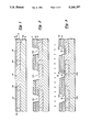
- FIGS. 1-7 are a series of cross-sectional views showing selective steps in fabricating a precision voltage reference in accordance with the present invention
- FIG. 8 is a plan view of the device of FIG. 5 taken along line 8--8 of FIG. 7;
- FIG. 9 is a schematic representation of the precision voltage reference in accordance with the present invention.
- FIG. 10 is a cross-section view of monolithic precision voltage reference incorporated into a larger monolithic integrated circuit.
- FIGS. 1-8 Fabrication of a precision voltage reference as a monolithic integrated circuit having selectively induced radiation compensation will be described in conjunction with FIGS. 1-8.
- the device to be described is based upon the use of a p-type doped silicon substrate material, it is to be understood that other substrate materials such as gallium arsenide, as well as n-type doped silicon substrate materials may alternatively be used.
- the equivalent device can be provided as an n-type silicon substrate material by reversing each of the dopant conductivities to be described herein and the voltage polarities provided to the device, as will be described in conjunction with FIG. 9.
- a substrate 12 comprised of silicon here doped p + type with a suitable p-type dopant such as boron to a concentration in the range of typically 5 ⁇ 10 18 to 10 19 atoms/cc or greater is shown to have disposed over a first surface 12a thereof a layer 14.
- layer 14 is an epitaxially grown layer also of silicon also doped p-type generally having the characteristic of a p dopant profile.
- a preferred range of dopant for layer 14 is 0.9 ⁇ 10 16 a/cc to 1.1 ⁇ 10 16 a/cc with 1 ⁇ 10 16 a/cc being a typically preferred value.
- Layer 15 is typically provided by heating layer 14 in a wet oxygen ambient atmosphere to a temperature of typically 1000° C.
- Layer 15 is generally provided having a thickness of 1200 ⁇ although any thickness in the range of 500 ⁇ to 3000 ⁇ may be used.
- Layer 14 is further provided with selectively doped p-type regions using conventional implant or diffusion techniques.
- selective masking layers are disposed over the upper surface of layer 14 and are patterned to expose underlying portions of the surface thereof such that additional p-type dopant material such as boron or boron difluoride (BF 2 ) can be selectively introduced to provide regions 14a.
- additional p-type dopant material such as boron or boron difluoride (BF 2 ) can be selectively introduced to provide regions 14a.
- masked regions 14, of layer 14 are as deposited p type silicon, whereas regions 14a are typically heavily doped p - type silicon having a dopant concentration in the range of 3 ⁇ 10 18 a/cc to 6 ⁇ 10 18 a/cc with 5 ⁇ 10 18 a/cc being a preferred value.
- Region 14a is here provided to prevent the formation of surface conducting channels between the two junctions which would compromise PVR voltage stability.
- the p-doping should be much lower than the doping concentration of the p+ region 14a so that the breakdown of the reverse-biased diode will be confined to the n+/p+ regions.
- the voltage across the junction is set by the n+ and p+ doping and the area of the p+ region.
- Each of these features are easily controlled during processing of the devices.
- current conduction occurs in the bulk, away from the Si-SiO 2 interface (layers 14, 15'), so that the voltage across the diode (not shown) is immune to surface effects which may be due to carrier injection into the oxide (a normal consequence of device operation) or radiation effects. If the n+ regions (not shown) were formed in a uniform p+ region, the breakdown would occur at the edges of the n+ region, where the electric fields are higher due to the curvature of the junction.
- the forward biased diode is provided as an annular junction about a central, second diode. That is, regions 14' and 14a are provided as incomplete and concentric annular regions or rings about a central, preferably circular, region (not numbered).
- the PVR may be provided as two diodes provided side by side on the substrate and disposed to occupy substantially rectangular plan areas. That is, rather than the junctions being circular they may be straight or linear.
- a layer 16 of an undoped glass i.e. amorphous SiO x
- a layer 16 of an undoped glass is deposited by any known technique over layer 15 (FIG. 2).
- a low pressure chemical vapor deposition technique is used.
- a masking layer (not numbered) is disposed over the undoped glass layer 16 and is patterned to provide patterned masking layer 17 having openings 17a and 17b selectively exposing (not shown) underlying portions of the undoped glass layer 16.
- the aperture 17a here is an incomplete annular aperture disposed about aperture 17b.
- exposed portions of the undoped glass layer 16 and underlying portions of thermal oxide layer 15 are selectively etched away leaving exposed portion of layer 14, as shown.
- thin oxide layers 18', 18" are provided typically by thermally oxidizing the exposed surface of layer 14 in a dry oxygen atmosphere at a temperature of 900° C., and here to a thickness of 200 ⁇ or generally less than the thickness of layer 15. Thereafter, a new masking layer 20 is disposed on layer 16.
- Layer 20 is patterned to expose portions of the thin oxide layers 18'and 18', A first aperture 20a, an incomplete annulus disposed about a second, central aperture 20b is provided with a transversal width such that all of the underlying thin oxide layer 18', as well as adjacent portions of layer 16 and 15, are exposed.
- aperture 20b is smaller than 18" by a sufficient amount so that the final p+ region 14d will be contained laterally within 18" when lateral diffusion from pocket 22b occurs. Worst-case misregistration between 18" and 20, and worst-case dimensional tolerances are taken into account when determining the dimension of aperture 20b. (Typically, the radius of the aperture 20b is 10 ⁇ m less than that of 18" which is about 90 ⁇ m.)
- the substrate is placed in an implantation field 22 of a suitable p-type dopant such as B or BF 2 and selective pockets 22a, 22b of said dopant are incorporated into the layer 14, as shown.
- substrate 12 is shown having p+ type regions 14b, 14d provided from the pockets 22a, 22b (FIG. 3).
- Regions 14b, 14d are provided by annealing substrate 12 after implantation of the B or BF 2 dopant species. Typically, annealing occurs at a temperature in the range of 950° C. to 1050° C. for 24 hours. Other conditions may be used.
- the pockets 22a, 22b are driven through layer 14 to provide the regions 14b, 14d, as shown.
- Regions 14b, 14d are p+ type and typically doped to a dopant concentration in the range of 1 ⁇ 10 18 a/cc to 3 ⁇ 10 18 a/cc. A typical dopant concentration for regions 14b, 14d is around 2 ⁇ 10 18 a/cc.
- Layer 14d, although being similarly doped as layer 14b, is physically separate from layer 14b, as will be described in conjunction with FIG. 7.
- regions 24a, 24b are shown and are selectively doped by ion implantation with an n-type dopant such as arsenic or phosphorus.
- regions 24a, 24b are doped to a concentration in the range of 5 ⁇ 10 19 a/cc to 1.5 ⁇ 10 20 a/cc with 1 ⁇ 10 20 a/cc being a preferred value.
- Regions 24a, 24b are defined by openings 16a, 16b provided in layers 16 and 15, as shown.
- the opening 16a is an incomplete annulus, as will be described in conjunction with FIG. 8, region 24a is likewise an incomplete annulus.
- n-type dopants After implanting of n-type dopants such dopants are activated by annealing the substrate at a temperature of 600° C. for 60 minutes followed by an anneal at 1000° C. for 40 minutes. This activates the n+ dopant and anneals out lattice damage caused by the implant process thus providing regions 24a, 24b.
- N-type region 24a is confined completely within region the p+ type doped region 14b whereas n-type region 24b extends beyond the underlying p+ type doped region 14d, as shown.
- This arrangement also prevents the formation of an n+/p- parasitic diode, which would steal current from the intended n+/p+ diode. This arrangement is used to reduce the effect of surface states on the operation of the diodes (not numbered), as will be further described.
- n+ type region 24a and underlying p-type region 14b provide a first pn junction Jl and, as will be described, forward biased diode 42 whereas n+ type region 24b and underlying p+ type region 14d provide a second pn junction J2 and, as will be described, reversed biased diode 44.
- a implant mask 28 here comprised of a suitable masking material such as photoresist is disposed over glass layer 16 and is patterned to provide an annular region 28a which exposes the underlying thin thermal oxide regions 18, Masking layer 28, however, is not patterned over the central portions of the device and thus protects the junction formed by layers 24b and 14d.
- the aperture 28a in masking layer 28 is made sufficiently large in lateral extent compared to the opening 16a in undoped glass layer 16 to insure that the implant mask does not partially obscure the opening 16a as could possibly occur due to misalignment tolerances. This is preferred to further insure that the functional characteristics of the forward junction will be properly modified by the implantation as will no be discussed.
- the substrate 12 is placed in the presence of an implantation field 30 of ion, nondopant species. Such species are implanted into the underlying junction regions and provide, in response, localized lattice damage as generally denoted by 30a.
- Preferred species for implantation field 30 include silicon, argon, carbon, fluorine, helium, hydrogen, nitrogen, and neon. Specific implantation schedules for each of the above-mentioned species is set forth in Table I below. Other implantation schedules are possible and are principally related to the total thickness of material through which the ions must penetrate, as well as the degree and character of the damage imparted to the junction area per implanted ion.
- layers 15' and 16 are chosen to be sufficient to prevent implanted species from penetrating through said layers 15' and 16 and to epitaxial layer 14.
- This schedule is selected to provide suitable damage at a junction about 200 ⁇ below a layer of silicon dioxide and 0.3 microns below the n-type silicon layer 14b. That is, it is preferred in this particular illustrative embodiment to place the atoms at the junction which is at a depth of approximately 0.32 microns.
- the presence of the implanted species 30a at the junction provide predetermined lattice damage to the junction of the first diode or pn region.
- This damage is the damage corresponding to that which would normally be provided to that junction during a specific radiation environment exposure.
- implanted silicon provides clusters of silicon atoms having energy states in the middle of the semiconductor bandgap. As a result, minority carrier lifetime is reduced within a limited depth in the silicon substrate.
- the region of perturbed lifetime at the junction can be selected so that it may influence the conduction mechanism of the forward biased diodes. This alters the forward junction radiation sensitivity and provides an optimized precision voltage reference which is also radiation hardened.
- the implant damage is provided at the junction regions. I should be pointed out, however, that the implantation step as shown in
- FIG. 6 should be provided after the last high temperature (i.e.>600° C.) anneal cycle and before metallization layers of substantial thicknesses are provided.
- high temperature i.e.>600° C.
- FIG. 6 should be provided after the last high temperature (i.e.>600° C.) anneal cycle and before metallization layers of substantial thicknesses are provided.
- exposure of the implanted substrate to a high temperature will cause annealing and thus removal of much of the damage induced at the junction, whereas providing metal layers of substantial thickness over the substrate will prevent implanted ions from reaching the desired location in the substrate.
- the stabilization anneal should occur at a temperature significantly above 100° C. to rapidly anneal out defects prone to healing at low temperatures, but less than 600° C. to retain a usable amount of the original implant damage at the junction.
- a specific stabilization anneal could be included in the process flow, but in the present case, the thermal cycles associated with subsequent processing steps--oxide deposition (420° C.), contact sinter (500° C.), hydrogen anneal (420° C.), and backside contact formation (450° C.)--are sufficient to provide the PVR with a defect structure which is sufficiently stable to provide the PVR with a 10 year operational lifetime in a typical application.
- a fabricated precision voltage reference 40 is shown to further include second and third layers 32, 34 of glass here each of said layers 32, 34 being doped with phosphorus providing a composite layer 33 and which are selectively deposited to passivate the device as is customary.
- layer 32 is provided over layer 15 and is patterned to provide windows to selectively expose underlying regions of thin oxide regions 18' and 18". Further, selective portions of the thin oxide layer 18', 18" are selectively etched away to expose underlying portions of layers 24a and 24b.
- a layer of platinum (not shown) is then deposited over layer 32 and within the window provided in layers 32, 18', 18" to thus contact regions 24a, 24b.
- the device is conventionally heated to a relatively low temperature of 500° C. to permit a platinum silicide to form and thus provide ohmic silicide contacts 36a, 36b to the n-type layers 24a, 24b.
- Other types of silicide contacts such as titanium and tungsten and so forth, of course, may alternatively be used.
- the unreacted platinum layer is removed by etching the platinum in aqua regia.
- a diffusion barrier layer (not shown) of a typical barrier material such as titanium tungsten alloy, for example, is deposited over layer 32 and is selectively patterned to provide isolated diffusion barrier regions 38a, 38b, as shown.
- Over layers 38a and 38b are provided aluminum contact metallizations 43a, 43b using conventional techniques such as evaporation or sputtering.
- Metallization layers provide external connection to the cathodes of the first and second pn junction 42, 44, respectively.
- the layer of doped glass 34 is deposited over device 40 to completely isolate the device as thus shown.
- the precision voltage reference 40 is shown formed on the substrate 12 having the epitaxially layer 14, oxide layer 15', undoped glass layer 16, and composite doped glass layer 33 (layers 32 and 34, FIG. 7).
- the precision voltage reference diodes 42, 44 are provided as a pair of concentric diodes with here the forward biased diode 42 provided as an incomplete annulus disposed about the central or reversed biased diode 44.
- This arrangement provides a shorter electrical connection between the anodes of the forward bias diode and reverse bias diode thus mitigating the amount of series resistance between the two diodes.
- a relatively large amount of series resistance will increase the noise of the diode and thus reduce its stability both as a function of variations in temperature, as well as during exposure to a radiation environment.
- the annular semiconductor regions of diode 42 which are disposed about diode 44 are an incomplete annulus permitting connection to the cathode of the second diode 44.
- the annular regions 14a, 14, and 14b (FIG. 1 and FIG. 6) are terminated such that region 14a is coupled to corresponding doped region 14c at the portion of the diode 40 where the annulus diode 42 is incomplete.
- regions 14b are coupled together to confine region 16a and region 14 is coupled together with corresponding region 14 on the opposing side of layer 16a.
- Contacts 50a and 50b are also provided typically during the same metal fabrication processes used to form layers 30a and 30b. Contact 50a is coupled to metal layer 43a whereas contact 50b is coupled to metal layer 42b. Conventional masking and etching processes are used to provide openings in the glass layer 42 over metal contacts 50a and 50b which permit attachment of metal bond wires to contacts 40a and 40b required to provide access to these contacts when the device is packaged. Contacts 50a and 50b are specifically provided away from the junction areas to prevent damage to the junctions which may be caused by the bonding operation.
- An optional ground plane conductor (FIG. 5 and FIG. 6) 52 is disposed on the backside of the substrate using conventional low temperature (i.e. less than 450° C.) techniques. It is also noted that often the substrate connection (i.e. the connection between the two anodes) is left floating (i.e. not connected to a potential).
- FIG. 9 a schematic representation of the device of FIG. 8 is shown to include a terminal 50a supported on substrate 12 coupled to a first diode 42 which is here a forward bias diode and thus corresponds to the outer annular diode region 42 of FIG. 8.
- the forward bias diode 42 has a region in the junction area having a predetermined lattice damage and clusters of, here, silicon atoms 30a disposed therein and as described above.
- Diode 42 is electrically connected to a reverse bias diode 44 via portions of substrate 12 as is illustrated in conjunction with FIG. 7. That is, the electrical path is provided between anode regions 14b and 14d through substrate layer 12 and optional conductor 52.
- the second diode 44 here the reverse biased diode 44 has its cathode coupled to a second terminal 50b disposed on substrate 12.
- terminal 50b is connected to a positive voltage potential and terminal 50a is connected to a negative voltage potential and typically to a reference potential such as ground.
- terminal 50b is provided a constant voltage which is substantially invariant with changes in temperature, as well as being substantially invariant with relatively high neutron fluence levels typically greater than 10 15 a/cm 2 .
- a precision voltage reference 40 as described in FIGS. 1-8, is shown incorporated as part of a larger monolithic integrated circuit 60.
- the integrated circuit 60 includes the precision voltage reference 40 generally described in conjunction with FIGS. 7 and 8 and other semiconductor circuits (not shown) such as, for example, bipolar transistor and complementary metal oxide semiconductor transistors (CMOS) generally referred to as (BiCMOS) circuits which may be arranged to provide a digital-to-analog converter and analog-to-digital converter or other functional integrated circuits.
- CMOS complementary metal oxide semiconductor transistors
- the integrated circuit 60 includes a substrate 62 here also comprised of silicon and here, for example, being doped n-type.
- P-well 63 is here shown isolating portions of an n-type epitaxial layer 64 disposed on substrate 62.
- the p-well is used to provide the p-type epilayer (14 FIG. 1) of the precision voltage reference.
- the fabrication steps for the precision voltage reference located in the p-well 63 are otherwise similar to the fabrication steps described in conjunction with FIGS. 1-8, except that the substrate 62 has an n-type dopant.
- a buried p++type layer 65 may be provided under the p-type well 63 formed in the n-type epitaxial layer 64 to reduce the parasitic series resistance between the forward and reverse biased junction.
- a p-well 63 in the BiCMOS integrated circuit as the p-type material for a precision voltage reference, such a reference may be incorporated into part of a larger circuit such as an analog-to-digital converter or digital-to-analog converter without substantially increasing the size of the circuit or interfering with the normal operation of the circuit.
- this arrangement provides a complete monolithic built-in voltage reference and functional circuit arrangement.
- An equivalent PVR could also be provided in an n-well on a p-substrate by reversing each of the dopant polarities and reversing the voltage applied to the device.
- each of the masking patterns used to define the respective structures would have or define rectangular regions rather than incomplete annulus regions.
- the basic fabrication techniques would otherwise be the same as described above.
- some empirical characterization of the effects of implant damage on junction voltages is preferably performed to achieve optimal radiation and temperature compensation.
- the change in breakdown voltage as a function of radiation dosage is obtained for various breakdown voltages. Similar data is also obtained for the forward biased junction.
- the appropriate dosage level of damage to the forward biased junction is matched to that of the appropriate reversed biased junction to provide the PVR with a radiation tolerance.
- the appropriate dosage level considering both radiation damage and temperature variations for the forward biased junction, is matched to a corresponding one for the reversed biased junction.
- the PVR in relation to the junction are of each of the diodes and the current density or, more particularly, the operating current through the PVR.
- the current density or, more particularly, the operating current through the PVR.
- variations in response to temperature changes and radiation exposure may be optimal for a particular operating current level through the PVR.
Landscapes
- Electrodes Of Semiconductors (AREA)
Abstract
Description
              TABLE I
______________________________________
Species      Dose (at/cm.sup.2)
                         Energy (KeV)
______________________________________
Silicon      1 × 10.sup.13
                         210
Argon        7 × 10.sup.12
                         335
Carbon       2 × 10.sup.13
                         150
Fluorine     1.5 × 10.sup.13
                         115
Helium       7 × 10.sup.13
                          40
Hydrogen     3 × 10.sup.14
                          20
Nitrogen     2 × 10.sup.13
                         140
Neon         1.5 × 10.sup.13
                         115
______________________________________
Claims (18)
Priority Applications (1)
| Application Number | Priority Date | Filing Date | Title |
|---|---|---|---|
| US07/783,432 US5146297A (en) | 1991-10-25 | 1991-10-25 | Precision voltage reference with lattice damage |
Applications Claiming Priority (1)
| Application Number | Priority Date | Filing Date | Title |
|---|---|---|---|
| US07/783,432 US5146297A (en) | 1991-10-25 | 1991-10-25 | Precision voltage reference with lattice damage |
Publications (1)
| Publication Number | Publication Date |
|---|---|
| US5146297A true US5146297A (en) | 1992-09-08 |
Family
ID=25129230
Family Applications (1)
| Application Number | Title | Priority Date | Filing Date |
|---|---|---|---|
| US07/783,432 Expired - Lifetime US5146297A (en) | 1991-10-25 | 1991-10-25 | Precision voltage reference with lattice damage |
Country Status (1)
| Country | Link |
|---|---|
| US (1) | US5146297A (en) |
Cited By (8)
| Publication number | Priority date | Publication date | Assignee | Title |
|---|---|---|---|---|
| US5466612A (en) * | 1992-03-11 | 1995-11-14 | Matsushita Electronics Corp. | Method of manufacturing a solid-state image pickup device |
| US5536680A (en) * | 1995-05-08 | 1996-07-16 | Texas Instruments Incorporated | Self-aligned bump bond infrared focal plane array architecture |
| US5729044A (en) * | 1992-06-30 | 1998-03-17 | Sgs-Thomson Microelectronics S.A. | Protection diode for a vertical semiconductor component |
| US5783973A (en) | 1997-02-24 | 1998-07-21 | The Charles Stark Draper Laboratory, Inc. | Temperature insensitive silicon oscillator and precision voltage reference formed therefrom |
| FR2812454A1 (en) * | 2000-07-27 | 2002-02-01 | Aeg Infrarot Module Gmbh | MULTISPECTRAL PHOTODIODE |
| US20090185316A1 (en) * | 2008-01-21 | 2009-07-23 | Jens Schneider | ESD/EOS Performance by Introduction of Defects |
| US20120139079A1 (en) * | 2010-11-16 | 2012-06-07 | Denso Corporation | Diode |
| CN113363310A (en) * | 2020-03-05 | 2021-09-07 | 意法半导体(图尔)公司 | Thyristor, triac and transient voltage suppressor diode fabrication |
Citations (5)
| Publication number | Priority date | Publication date | Assignee | Title |
|---|---|---|---|---|
| US4353754A (en) * | 1979-08-06 | 1982-10-12 | Mitsubishi Denki Kabushiki Kaisha | Thermo-sensitive switching element manufacturing method |
| JPS5922368A (en) * | 1982-07-28 | 1984-02-04 | Hitachi Ltd | Zener diode and its manufacturing method |
| US4689667A (en) * | 1985-06-11 | 1987-08-25 | Fairchild Semiconductor Corporation | Method of controlling dopant diffusion and dopant electrical activation by implanted inert gas atoms |
| US4905060A (en) * | 1987-05-29 | 1990-02-27 | Hitachi, Ltd. | Light emitting device with disordered region |
| US4948989A (en) * | 1989-01-31 | 1990-08-14 | Science Applications International Corporation | Radiation-hardened temperature-compensated voltage reference |
-
1991
- 1991-10-25 US US07/783,432 patent/US5146297A/en not_active Expired - Lifetime
Patent Citations (5)
| Publication number | Priority date | Publication date | Assignee | Title |
|---|---|---|---|---|
| US4353754A (en) * | 1979-08-06 | 1982-10-12 | Mitsubishi Denki Kabushiki Kaisha | Thermo-sensitive switching element manufacturing method |
| JPS5922368A (en) * | 1982-07-28 | 1984-02-04 | Hitachi Ltd | Zener diode and its manufacturing method |
| US4689667A (en) * | 1985-06-11 | 1987-08-25 | Fairchild Semiconductor Corporation | Method of controlling dopant diffusion and dopant electrical activation by implanted inert gas atoms |
| US4905060A (en) * | 1987-05-29 | 1990-02-27 | Hitachi, Ltd. | Light emitting device with disordered region |
| US4948989A (en) * | 1989-01-31 | 1990-08-14 | Science Applications International Corporation | Radiation-hardened temperature-compensated voltage reference |
Cited By (18)
| Publication number | Priority date | Publication date | Assignee | Title |
|---|---|---|---|---|
| US5466612A (en) * | 1992-03-11 | 1995-11-14 | Matsushita Electronics Corp. | Method of manufacturing a solid-state image pickup device |
| US5729044A (en) * | 1992-06-30 | 1998-03-17 | Sgs-Thomson Microelectronics S.A. | Protection diode for a vertical semiconductor component |
| US5536680A (en) * | 1995-05-08 | 1996-07-16 | Texas Instruments Incorporated | Self-aligned bump bond infrared focal plane array architecture |
| US5783973A (en) | 1997-02-24 | 1998-07-21 | The Charles Stark Draper Laboratory, Inc. | Temperature insensitive silicon oscillator and precision voltage reference formed therefrom |
| FR2812454A1 (en) * | 2000-07-27 | 2002-02-01 | Aeg Infrarot Module Gmbh | MULTISPECTRAL PHOTODIODE |
| US6525387B2 (en) * | 2000-07-27 | 2003-02-25 | Aeg Infrarot-Module Gmbh | Multispectral photodiode |
| US10756081B2 (en) | 2008-01-21 | 2020-08-25 | Infineon Technologies Ag | Avalanche diode having an enhanced defect concentration level and method of making the same |
| US8791547B2 (en) | 2008-01-21 | 2014-07-29 | Infineon Technologies Ag | Avalanche diode having an enhanced defect concentration level and method of making the same |
| US9257523B2 (en) | 2008-01-21 | 2016-02-09 | Infineon Technologies Ag | Avalanche diode having an enhanced defect concentration level and method of making the same |
| US9812438B2 (en) | 2008-01-21 | 2017-11-07 | Infineon Technologies Ag | Avalanche diode having an enhanced defect concentration level and method of making the same |
| US20090185316A1 (en) * | 2008-01-21 | 2009-07-23 | Jens Schneider | ESD/EOS Performance by Introduction of Defects |
| US20120139079A1 (en) * | 2010-11-16 | 2012-06-07 | Denso Corporation | Diode |
| US8476673B2 (en) * | 2010-11-16 | 2013-07-02 | Denso Corporation | Diode |
| CN113363310A (en) * | 2020-03-05 | 2021-09-07 | 意法半导体(图尔)公司 | Thyristor, triac and transient voltage suppressor diode fabrication |
| EP3876288A1 (en) * | 2020-03-05 | 2021-09-08 | STMicroelectronics (Tours) SAS | Formation of a thyristor, triac or diode for suppressing transient voltages |
| FR3107988A1 (en) * | 2020-03-05 | 2021-09-10 | Stmicroelectronics (Tours) Sas | Formation of a thyristor, triac or transient voltage suppression diode |
| US11610988B2 (en) | 2020-03-05 | 2023-03-21 | Stmicroelectronics (Tours) Sas | Thyristor, triac and transient-voltage-suppression diode manufacturing |
| US12230698B2 (en) | 2020-03-05 | 2025-02-18 | Stmicroelectronics (Tours) Sas | Thyristor, triac and transient-voltage-suppression diode manufacturing |
Similar Documents
| Publication | Publication Date | Title |
|---|---|---|
| US4203126A (en) | CMOS structure and method utilizing retarded electric field for minimum latch-up | |
| US5024965A (en) | Manufacturing high speed low leakage radiation hardened CMOS/SOI devices | |
| US4298401A (en) | Breakdown voltage resistor obtained through a double ion-implantation into a semiconductor substrate, and manufacturing process of the same | |
| US4769686A (en) | Semiconductor device | |
| US5341022A (en) | Bipolar transistor having a high ion concentration buried floating collector and method of fabricating the same | |
| US4948989A (en) | Radiation-hardened temperature-compensated voltage reference | |
| US4263518A (en) | Arrangement for correcting the voltage coefficient of resistance of resistors integral with a semiconductor body | |
| JPH0680688B2 (en) | Planar semiconductor device body and its manufacturing method | |
| US4466171A (en) | Method of manufacturing a semiconductor device utilizing outdiffusion to convert an epitaxial layer | |
| KR0166052B1 (en) | High Voltage Merge Bipolar / CMOS and Its Manufacturing Method | |
| US5907168A (en) | Low noise Ge-JFETs | |
| US5146297A (en) | Precision voltage reference with lattice damage | |
| US5264721A (en) | Insulated-gate FET on an SOI-structure | |
| US4432008A (en) | Gold-doped IC resistor region | |
| US5242849A (en) | Method for the fabrication of MOS devices | |
| US6583485B2 (en) | Schottky diode | |
| US4041519A (en) | Low transient effect switching device and method | |
| US5543647A (en) | Semiconductor device having a plurality of impurity layers | |
| US5731637A (en) | Semiconductor device | |
| JPH04363046A (en) | Manufacture of semiconductor device | |
| EP0974165B1 (en) | Semiconductor device with a bipolar transistor, and method of manufacturing such a device | |
| US5734194A (en) | Semiconductor device and method of making | |
| EP0101739B1 (en) | Heterojunction transistor and method of fabricating the same | |
| JPS63192274A (en) | Improved Schottky barrier diode for alpha particle resistant static random access memory | |
| EP0109888A2 (en) | Subsurface Zener diode |
Legal Events
| Date | Code | Title | Description |
|---|---|---|---|
| AS | Assignment |
Owner name: RAYTHEON COMPANY, MASSACHUSETTS Free format text: ASSIGNMENT OF ASSIGNORS INTEREST.;ASSIGNORS:COLLINS, STEVEN R.;JOHNSON, ROBERT B.;REEL/FRAME:005907/0846 Effective date: 19911025 |
|
| STCF | Information on status: patent grant |
Free format text: PATENTED CASE |
|
| FEPP | Fee payment procedure |
Free format text: PAYOR NUMBER ASSIGNED (ORIGINAL EVENT CODE: ASPN); ENTITY STATUS OF PATENT OWNER: LARGE ENTITY |
|
| FPAY | Fee payment |
Year of fee payment: 4 |
|
| FEPP | Fee payment procedure |
Free format text: PAYER NUMBER DE-ASSIGNED (ORIGINAL EVENT CODE: RMPN); ENTITY STATUS OF PATENT OWNER: LARGE ENTITY Free format text: PAYOR NUMBER ASSIGNED (ORIGINAL EVENT CODE: ASPN); ENTITY STATUS OF PATENT OWNER: LARGE ENTITY |
|
| FPAY | Fee payment |
Year of fee payment: 8 |
|
| FEPP | Fee payment procedure |
Free format text: PAYER NUMBER DE-ASSIGNED (ORIGINAL EVENT CODE: RMPN); ENTITY STATUS OF PATENT OWNER: LARGE ENTITY Free format text: PAYOR NUMBER ASSIGNED (ORIGINAL EVENT CODE: ASPN); ENTITY STATUS OF PATENT OWNER: LARGE ENTITY |
|
| FPAY | Fee payment |
Year of fee payment: 12 |