US5136478A - Solid electrolyte capacitor and method of making - Google Patents
Solid electrolyte capacitor and method of making Download PDFInfo
- Publication number
- US5136478A US5136478A US07/770,624 US77062491A US5136478A US 5136478 A US5136478 A US 5136478A US 77062491 A US77062491 A US 77062491A US 5136478 A US5136478 A US 5136478A
- Authority
- US
- United States
- Prior art keywords
- layer
- anode
- silver
- electrolyte
- rbag
- Prior art date
- Legal status (The legal status is an assumption and is not a legal conclusion. Google has not performed a legal analysis and makes no representation as to the accuracy of the status listed.)
- Expired - Fee Related
Links
- 239000003990 capacitor Substances 0.000 title claims abstract description 53
- 239000007784 solid electrolyte Substances 0.000 title claims abstract description 17
- 238000004519 manufacturing process Methods 0.000 title description 15
- 229910052709 silver Inorganic materials 0.000 claims abstract description 105
- 239000004332 silver Substances 0.000 claims abstract description 105
- OKTJSMMVPCPJKN-UHFFFAOYSA-N Carbon Chemical compound [C] OKTJSMMVPCPJKN-UHFFFAOYSA-N 0.000 claims abstract description 97
- BQCADISMDOOEFD-UHFFFAOYSA-N Silver Chemical compound [Ag] BQCADISMDOOEFD-UHFFFAOYSA-N 0.000 claims abstract description 89
- 239000003792 electrolyte Substances 0.000 claims abstract description 86
- 210000001787 dendrite Anatomy 0.000 claims abstract description 56
- 238000000034 method Methods 0.000 claims abstract description 22
- 238000003860 storage Methods 0.000 claims abstract description 9
- 239000002001 electrolyte material Substances 0.000 claims abstract description 8
- -1 silver ions Chemical class 0.000 claims description 22
- 229910052751 metal Inorganic materials 0.000 claims description 14
- 239000002184 metal Substances 0.000 claims description 14
- 230000005684 electric field Effects 0.000 claims description 6
- 238000009825 accumulation Methods 0.000 claims description 2
- 230000035508 accumulation Effects 0.000 claims description 2
- 239000007773 negative electrode material Substances 0.000 claims 7
- 239000007774 positive electrode material Substances 0.000 claims 2
- 229910052799 carbon Inorganic materials 0.000 abstract description 45
- 239000000463 material Substances 0.000 abstract description 17
- 238000007599 discharging Methods 0.000 abstract description 13
- 239000010405 anode material Substances 0.000 abstract description 6
- 239000010406 cathode material Substances 0.000 abstract description 6
- 239000010410 layer Substances 0.000 description 148
- 210000004027 cell Anatomy 0.000 description 46
- 238000010586 diagram Methods 0.000 description 24
- 239000004020 conductor Substances 0.000 description 23
- 230000006835 compression Effects 0.000 description 19
- 238000007906 compression Methods 0.000 description 19
- 239000000843 powder Substances 0.000 description 18
- BASFCYQUMIYNBI-UHFFFAOYSA-N platinum Chemical compound [Pt] BASFCYQUMIYNBI-UHFFFAOYSA-N 0.000 description 16
- 239000011230 binding agent Substances 0.000 description 12
- 238000007747 plating Methods 0.000 description 11
- 239000002245 particle Substances 0.000 description 10
- 238000004146 energy storage Methods 0.000 description 9
- 230000007246 mechanism Effects 0.000 description 9
- 230000005012 migration Effects 0.000 description 9
- 238000013508 migration Methods 0.000 description 9
- 230000006870 function Effects 0.000 description 8
- 239000011630 iodine Substances 0.000 description 8
- 229910052740 iodine Inorganic materials 0.000 description 8
- 229910052697 platinum Inorganic materials 0.000 description 8
- 230000002093 peripheral effect Effects 0.000 description 7
- 238000004804 winding Methods 0.000 description 7
- 229920004142 LEXAN™ Polymers 0.000 description 6
- 239000004418 Lexan Substances 0.000 description 6
- 230000008569 process Effects 0.000 description 6
- 239000000203 mixture Substances 0.000 description 5
- 239000002904 solvent Substances 0.000 description 5
- CSCPPACGZOOCGX-UHFFFAOYSA-N Acetone Chemical compound CC(C)=O CSCPPACGZOOCGX-UHFFFAOYSA-N 0.000 description 4
- ZOKXTWBITQBERF-UHFFFAOYSA-N Molybdenum Chemical compound [Mo] ZOKXTWBITQBERF-UHFFFAOYSA-N 0.000 description 4
- JUJWROOIHBZHMG-UHFFFAOYSA-N Pyridine Chemical compound C1=CC=NC=C1 JUJWROOIHBZHMG-UHFFFAOYSA-N 0.000 description 4
- 229910021612 Silver iodide Inorganic materials 0.000 description 4
- FOIXSVOLVBLSDH-UHFFFAOYSA-N Silver ion Chemical compound [Ag+] FOIXSVOLVBLSDH-UHFFFAOYSA-N 0.000 description 4
- 229910052750 molybdenum Inorganic materials 0.000 description 4
- 239000011733 molybdenum Substances 0.000 description 4
- NJPPVKZQTLUDBO-UHFFFAOYSA-N novaluron Chemical compound C1=C(Cl)C(OC(F)(F)C(OC(F)(F)F)F)=CC=C1NC(=O)NC(=O)C1=C(F)C=CC=C1F NJPPVKZQTLUDBO-UHFFFAOYSA-N 0.000 description 4
- ZCYVEMRRCGMTRW-UHFFFAOYSA-N 7553-56-2 Chemical compound [I] ZCYVEMRRCGMTRW-UHFFFAOYSA-N 0.000 description 3
- 238000010276 construction Methods 0.000 description 3
- 239000003870 refractory metal Substances 0.000 description 3
- 239000002356 single layer Substances 0.000 description 3
- 239000007787 solid Substances 0.000 description 3
- 125000006850 spacer group Chemical group 0.000 description 3
- IJGRMHOSHXDMSA-UHFFFAOYSA-N Atomic nitrogen Chemical compound N#N IJGRMHOSHXDMSA-UHFFFAOYSA-N 0.000 description 2
- 239000004593 Epoxy Substances 0.000 description 2
- KDLHZDBZIXYQEI-UHFFFAOYSA-N Palladium Chemical compound [Pd] KDLHZDBZIXYQEI-UHFFFAOYSA-N 0.000 description 2
- 229910001315 Tool steel Inorganic materials 0.000 description 2
- 230000015572 biosynthetic process Effects 0.000 description 2
- 230000001680 brushing effect Effects 0.000 description 2
- 238000000576 coating method Methods 0.000 description 2
- 230000001351 cycling effect Effects 0.000 description 2
- 229910001873 dinitrogen Inorganic materials 0.000 description 2
- 230000000694 effects Effects 0.000 description 2
- 238000002474 experimental method Methods 0.000 description 2
- 150000002500 ions Chemical class 0.000 description 2
- 238000005259 measurement Methods 0.000 description 2
- 239000002923 metal particle Substances 0.000 description 2
- 239000004570 mortar (masonry) Substances 0.000 description 2
- 239000005022 packaging material Substances 0.000 description 2
- 239000004033 plastic Substances 0.000 description 2
- UMJSCPRVCHMLSP-UHFFFAOYSA-N pyridine Natural products COC1=CC=CN=C1 UMJSCPRVCHMLSP-UHFFFAOYSA-N 0.000 description 2
- 229910052701 rubidium Inorganic materials 0.000 description 2
- IGLNJRXAVVLDKE-UHFFFAOYSA-N rubidium atom Chemical compound [Rb] IGLNJRXAVVLDKE-UHFFFAOYSA-N 0.000 description 2
- 229910001220 stainless steel Inorganic materials 0.000 description 2
- 239000010935 stainless steel Substances 0.000 description 2
- JKFYKCYQEWQPTM-UHFFFAOYSA-N 2-azaniumyl-2-(4-fluorophenyl)acetate Chemical compound OC(=O)C(N)C1=CC=C(F)C=C1 JKFYKCYQEWQPTM-UHFFFAOYSA-N 0.000 description 1
- 239000004677 Nylon Substances 0.000 description 1
- 241000316887 Saissetia oleae Species 0.000 description 1
- 229910000831 Steel Inorganic materials 0.000 description 1
- RTAQQCXQSZGOHL-UHFFFAOYSA-N Titanium Chemical compound [Ti] RTAQQCXQSZGOHL-UHFFFAOYSA-N 0.000 description 1
- 230000001464 adherent effect Effects 0.000 description 1
- 229910052783 alkali metal Inorganic materials 0.000 description 1
- 150000001340 alkali metals Chemical class 0.000 description 1
- 238000010420 art technique Methods 0.000 description 1
- 230000004888 barrier function Effects 0.000 description 1
- 239000002585 base Substances 0.000 description 1
- 230000006399 behavior Effects 0.000 description 1
- 230000003197 catalytic effect Effects 0.000 description 1
- 210000005056 cell body Anatomy 0.000 description 1
- 230000008859 change Effects 0.000 description 1
- 239000011248 coating agent Substances 0.000 description 1
- 239000002131 composite material Substances 0.000 description 1
- 239000000470 constituent Substances 0.000 description 1
- 230000006378 damage Effects 0.000 description 1
- 230000007423 decrease Effects 0.000 description 1
- 230000003247 decreasing effect Effects 0.000 description 1
- 230000000593 degrading effect Effects 0.000 description 1
- 230000000779 depleting effect Effects 0.000 description 1
- 238000009792 diffusion process Methods 0.000 description 1
- 238000009713 electroplating Methods 0.000 description 1
- 230000003628 erosive effect Effects 0.000 description 1
- 238000001704 evaporation Methods 0.000 description 1
- 230000008020 evaporation Effects 0.000 description 1
- 238000001914 filtration Methods 0.000 description 1
- 239000012530 fluid Substances 0.000 description 1
- 229910002804 graphite Inorganic materials 0.000 description 1
- 239000010439 graphite Substances 0.000 description 1
- 238000010438 heat treatment Methods 0.000 description 1
- 239000010416 ion conductor Substances 0.000 description 1
- 238000002955 isolation Methods 0.000 description 1
- 239000011159 matrix material Substances 0.000 description 1
- 238000002844 melting Methods 0.000 description 1
- 230000008018 melting Effects 0.000 description 1
- 230000005055 memory storage Effects 0.000 description 1
- 238000012986 modification Methods 0.000 description 1
- 230000004048 modification Effects 0.000 description 1
- 229910000510 noble metal Inorganic materials 0.000 description 1
- 229920001778 nylon Polymers 0.000 description 1
- 238000004806 packaging method and process Methods 0.000 description 1
- 229910052763 palladium Inorganic materials 0.000 description 1
- 229920001296 polysiloxane Polymers 0.000 description 1
- 238000003825 pressing Methods 0.000 description 1
- 230000009467 reduction Effects 0.000 description 1
- 238000007789 sealing Methods 0.000 description 1
- 238000000926 separation method Methods 0.000 description 1
- 229940045105 silver iodide Drugs 0.000 description 1
- 230000007480 spreading Effects 0.000 description 1
- 238000003892 spreading Methods 0.000 description 1
- 239000010959 steel Substances 0.000 description 1
- 239000000126 substance Substances 0.000 description 1
- 229910052715 tantalum Inorganic materials 0.000 description 1
- GUVRBAGPIYLISA-UHFFFAOYSA-N tantalum atom Chemical compound [Ta] GUVRBAGPIYLISA-UHFFFAOYSA-N 0.000 description 1
- 238000012360 testing method Methods 0.000 description 1
- 229910052719 titanium Inorganic materials 0.000 description 1
- 239000010936 titanium Substances 0.000 description 1
Images


Classifications
-
- H—ELECTRICITY
- H01—ELECTRIC ELEMENTS
- H01G—CAPACITORS; CAPACITORS, RECTIFIERS, DETECTORS, SWITCHING DEVICES, LIGHT-SENSITIVE OR TEMPERATURE-SENSITIVE DEVICES OF THE ELECTROLYTIC TYPE
- H01G9/00—Electrolytic capacitors, rectifiers, detectors, switching devices, light-sensitive or temperature-sensitive devices; Processes of their manufacture
- H01G9/004—Details
- H01G9/022—Electrolytes; Absorbents
- H01G9/025—Solid electrolytes
-
- Y—GENERAL TAGGING OF NEW TECHNOLOGICAL DEVELOPMENTS; GENERAL TAGGING OF CROSS-SECTIONAL TECHNOLOGIES SPANNING OVER SEVERAL SECTIONS OF THE IPC; TECHNICAL SUBJECTS COVERED BY FORMER USPC CROSS-REFERENCE ART COLLECTIONS [XRACs] AND DIGESTS
- Y02—TECHNOLOGIES OR APPLICATIONS FOR MITIGATION OR ADAPTATION AGAINST CLIMATE CHANGE
- Y02E—REDUCTION OF GREENHOUSE GAS [GHG] EMISSIONS, RELATED TO ENERGY GENERATION, TRANSMISSION OR DISTRIBUTION
- Y02E60/00—Enabling technologies; Technologies with a potential or indirect contribution to GHG emissions mitigation
- Y02E60/13—Energy storage using capacitors
Definitions
- the invention relates to a highly reliable solid electrolyte capacitor and method of making, and more particularly to a solid electrolyte capacitor including an anode and cathode each composed of carbon and RbAg 4 I 5 and a solid electrolyte composed of RbAg 4 I 5 , and also to a method of using the capacitor in a pseudocapacitance mode to increase energy storage without causing dendrite growth that would electrically short the anode of the capacitor to the cathode thereof.
- anode will be used for the negative electrode and the term “cathode” will be used for the positive electrode, even though this terminology is strictly correct only for the discharge process.
- Such solid-state cells generally utilize silver as anode material and carbon capable of functioning as an electron receptor material for the cathode material.
- the solid electrolyte serves as an ionic conductor for the ionic part of the current within the solid-state cell.
- U.S. Pat. Nos. 3,701,685, 3,503,810, 3,443,997, 3,476,605, 3,647,549, 3,663,299, and 3,476,606 are generally indicative of the state of the art for such solid-state cells.
- the first reference mentioned above describes a supercapacitor, on page 20, as one of the type under discussion charged to a voltage below 0.50 volts wherein silver is plated on silver already present in the anode during charging and a layer of electrons is formed on the surface of carbon contained in the cathode during the charging operation.
- the second reference mentioned above describes the same supercapacitor cell, being charged to levels in the range from 0.50 volts to 0.65 volts.
- the same structure in this case is referred to as a "pseudocapacitor" wherein more of the silver is plated onto the anode, and in the cathode a monolayer of iodine ions is postulated to form on the surface of carbon contained in the cathode material.
- This has the result of increasing the energy storage by a factor of approximately 5 over the energy storage in the same supercapacitor structure if no iodine is being plated onto the cathode. This increase is postulated to result from the decreased dielectric separation.
- the electrochemical capacitor disclosed in the above references uses the highly conducting solid electrolyte RbAg 4 I 5 .
- the anode of the basic cell system is composed of silver/RbAg 4 I 5 /carbon.
- the silver in the anode behaves as an electrode with very high capacitance, because the overvoltage necessary to plate silver on silver is very low.
- the RbAg 4 I 5 is oxidized to form a monolayer of iodine at the carbon/electrolyte interface in the electrolyte contained in the cathode.
- the charge is stored as electrons on the surface of the carbon of the cathode.
- the current decays to near zero as the required activity of iodine is established at the carbon/electrolyte surface.
- a voltage in the range of 0.50 volts to 0.65 volts is applied between the cathode and anode, its charging behavior changes and this is termed the "pseudocapacitance" region of the solid-state cell's capacitance characteristic.
- potentials greater than 0.66 volts the electrolyte is decomposed.
- the total energy stored in the solid-state cell increases to about 5 times that stored in the double layer region.
- capacitor 1 has an anode 2 composed of activated carbon, silver and RbAg 4 I 5 .
- Anode 2 is connected by a conductor 3 to a negative voltage.
- Anode 2 abuts a solid dielectric 4 composed of pure RbAg 4 I 5 .
- the opposite face of solid electrolyte 4 contacts a cathode 5 composed of activated carbon and RbAg 4 I 5 .
- capacitor 1 In prior art capacitor 1, the material of anode 2, solid electrolyte 4, and cathode 5 all include approximately one to two percent uniformly distributed LEXAN plastic material which serves as a binder for the particles of carbon and RbAg 4 I 5 of which capacitor 1 is composed.
- Capacitor 1 of FIG. 1 is referred to as a "polar" structure because the anode and cathode are separately composed as described above for a specific polarity.
- FIG. 1A illustrates growth of such silver dendrites, which cause capacitor failure by short circuiting the anode and the cathode together.
- segment 30A designates what is referred to herein as the "double layer” operating region of capacitor 1 and segment 30B is referred to herein as the "pseudocapacitor" operating region.
- the charging circuit of capacitor 1 includes silver ions (Ag + ) flowing in the direction of arrow 7 from RbAg 4 I 5 electrolyte layer 4 to anode layer 2.
- the charging current also includes electrons (e - ) flowing in the direction of arrow 8 from electrolyte 4 to cathode 5.
- a monolayer of such electrons are thought to become "plated” on activated carbon surface areas such as 15, possibly with a several angstrom gap maintained by molecular repulsive forces.
- the capacitance produced by the above mechanism is indicated by capacitor 19 in the schematic diagram of FIG. 3.
- FIG. 3 designates a schematic equivalent diagram of the capacitance of the supercapacitor 1 shown in FIG. 1.
- Capacitor 19 represents the "double layer capacitance” and capacitor 20 designates the "pseudocapacitance”.
- Approximately eighty percent of the energy storage capacity of capacitor 1 is in the "pseudocapacitance" range 30B of FIG. 2 when capacitor 1 is charged to a voltage of approximately 0.65 volts and twenty percent is in the "double layer” region 30A of FIG. 2 when capacitor 1 is charged to 0.50 volts.
- charge storage is thought to be due to accumulation of iodine ions on carbon surfaces of cathode 5.
- the LEXAN binders mentioned above are thought to produce grains or growth paths in capacitor 1, particularly in RbAg 4 I 5 of electrolyte 4, which encourage growth of the above-mentioned silver dendrites.
- Such silver dendrites illustrated by numeral 21 in FIG. 1A, may result in the primary failure mechanism of the prior art cell of FIG. 1.
- the invention provides a technique for supplying a backup voltage, including providing a solid-state electrochemical capacitor structure with a solid electrolyte composed of a layer of RbAg 4 I 5 , an anode composed of a layer of carbon and RbAg 4 I 5 on a first surface of the electrolyte, and a cathode composed of a layer of carbon and RbAg 4 I 5 on a second surface of the electrolyte.
- a current is supplied to charge the cathode of the capacitor structure to a voltage in the range from 0.50 volts to 0.66 volts to cause storage of charge in the capacitor structure in both a double layer capacitance mode and a pseudo capacitance mode.
- the charged up capacitor is used to supply a backup voltage to a CMOS memory.
- the capacitor structure is made by compressing the electrolyte, the anode, and the cathode together to produce physical bonding without binder material, using compression forces of more than approximately eighty thousand psi.
- the capacitor structures of the invention imply silver plating on an interface between the electrolyte and the carbon of the anode, whereby silver is presumably depleted from the electrolyte. All embodiments are designed to prevent or reduce growth of dendrites through or around the electrolyte layer which cause failure of the capacitor structure.
- the anode is composed of a silver disk adjoining a surface of the electrolyte.
- the anode includes platinized carbon which acts to perform a stable plating surface for migrating silver ions during the cell charging process, so as to greatly minimize formation of silver dendrites during the charging cycle.
- the anode layer is composed of stable, silver-platable metal particles in sufficient concentration to substantially inhibit growth of silver dendrites during charging of the capacitor structure.
- the anode includes varying concentrations of silver, the variation being selected to reduce dendrite growth and/or confine it to within the body of the anode during the charging process.
- the electrolyte is formed by spreading a paste composed of electrolyte powder dissolved in solvent on a cathode surface (formed of activated carbon and RbAg 4 I 5 ) so as to fill gaps in an insulating spacer.
- a silver anode disk is pressed into the paste, and is kept separated from the cathode by the insulating spacer to form the anode.
- the solvent evaporates to produce a rigid pseudocapacitor structure.
- a circuit and technique is described for charging a plurality of pseudocapacitors in parallel so that all are charged to precisely the same voltage, up to 0.66 volts.
- the circuit connects the pseudocapacitors in series to supply a backup voltage to a utilization device.
- a plurality of pseudocapacitors are connected in parallel, and the voltage across them is applied to the input of a DC-to-DC converter to provide a boosted DC output voltage.
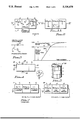
- FIG. 1 is a diagram of a prior art supercapacitor.
- FIG. 1A is a diagram that illustrates dendrite growth and the way such dendrites cause failure of prior solid-state supercapacitor structures.
- FIG. 2 is a graph useful in describing two modes of operating the prior art capacitor of FIG. 1.
- FIG. 3 is a schematic diagram showing an equivalent circuit for the structure of FIG. 1 operated in accordance with FIG. 2.
- FIG. 4 is a diagram of the supercapacitor of one embodiment of the present invention before removal of peripheral dendrites.
- FIG. 5 is a perspective view of a supercapacitor of the present invention.
- FIG. 6 is a diagram of an apparatus used in making the supercapacitor of FIG. 5.
- FIG. 6A is a partial section diagram of the die and compression members used to make the supercapacitor of FIG. 4.
- FIG. 7 is a diagram useful in comparing one embodiment of the supercapacitor of the present invention with the prior art supercapacitor of FIG. 1.
- FIG. 8 is a diagram of a stack of the supercapacitors of the invention connected to provide a backup battery for a CMOS memory.
- FIG. 9 is a diagram of an embodiment of the invention designed to provide a large discharge current.
- FIGS. 10A and 10B are flow diagrams of the method of making the supercapacitor of FIG. 4.
- FIG. 11A is a diagram of another embodiment of the invention including platinized carbon in the anode.
- FIG. 11B is a diagram of another embodiment of the invention including a graded anode structure including platinized carbon, varying amounts of silver, and a pure silver contact layer.
- FIG. 12 is a diagram of an embodiment of the invention in which the anode is composed of pure silver or other metal with low silver plating overvoltage.
- FIG. 13 is a diagram of another embodiment of the invention with a reduced-size anode of pure silver.
- FIG. 14 is a diagram of another embodiment of the invention in which the anode includes a layer of platinized carbon and RbAg 4 I 5 and a reduced-size layer of pure silver.
- FIG. 15 is a diagram of another embodiment of the invention in which the electrolyte layer is formed from paste composed of RbAg 4 I 5 particles.
- FIG. 15A is a diagram of an embodiment of the invention convenient for packaging serially connected pseudocapacitors.
- FIG. 16A is a diagram illustrating a proposed charging mechanism of the pseudocapacitor of the present invention.
- FIG. 16B is a diagram illustrating discharging the pseudocapacitor of the invention.
- FIG. 17A is a diagram of a parallel charging, serial discharging technique for a backup power source including multiple pseudocapacitors of the invention.
- FIG. 17B is a circuit diagram illustrating a practical implementation of the structure shown in FIG. 17A.
- FIG. 18 is a perspective view of a package containing the invention suitable for use as a backup power supply for a volatile memory system.
- FIG. 19 is a diagram showing parallel connection of a number of pseudocapacitors of the present invention and use of a DC-to-DC converter to boost the pseudocapacitor voltage to a higher voltage.
- an initially nonpolar "supercapacitor" 25 made in accordance with one embodiment of the present invention, is referred to as "non-polar" because anode 2 and cathode 5 are of identical composition.
- Both anode 2 and cathode 5 are composed of activated carbon and RbAg 4 I 5 , and are formed by very high pressure compression, of the order of a 80,000 pounds per square inch (or lower pressure if the temperature of the material is increased).
- dendrites 26 eventually adjusts composition of the cell by depleting silver ion concentration in solid electrolyte 4.
- the dendrites thus formed are removed by brushing them away, no further failure mechanism due to dendrite growth can occur because of the depleted silver ion concentration in electrolyte layer 4. Consequently, a very temperature-stable, long life pseudocapacitor cell is obtained.
- pseudocapacitor 25 can be discharged many thousands of times without affecting reliability or performance thereof. (Dendrites may also grow internally, but as long as they do not extend from the anode to the cathode, they do not effect the reliability or performance of pseudocapacitor 25.)
- pseudocapacitor 25 operates as a capacitance in the double layer mode and in the pseudocapacitance mode is the same as described in the above-mentioned Oxley references.
- the prior art discloses operating only in the double layer region 30A of the curve of FIG. 2. Mr. Oxley claimed that this structure described in his articles could not be operated in the pseudocapacitance mode. (Perhaps because the non-polar structure of the prior art supercapacitor structure which is identical to that of pseudocapacitor 25 has only half of the capacitance of a similar polar supercapacitor structure, and perhaps also because charging operation would be inefficient with no distributed silver in the anode for silver ions from the electrolyte layer 4 to plate onto).
- operating the nonpolar structure in the pseudocapacitance mode by charging it to voltages close to 0.65 volts causes peripheral dendrite growth which may deplete silver to the point where there is none left for producing internal dendrite growth sufficient to cause device failure due to cathode-to-anode shorting.
- the external dendrites 26 can be removed by brushing.
- the construction of the pseudocapacitor 25 probably enhances growth of peripheral dendrites substantially faster than internal dendrites, causing depletion of silver before any internal dendrites grow far enough from the anode to produce an electrical short to the cathode.
- the capacitance of nonpolar capacitor 25 operated in the double layer region is one-half that of a polar cell because the anode and cathode capacitive layers are coupled in series).
- FIG. 7 illustrates the distinguishing features of one embodiment of the present invention.
- the pseudocapacitor 25 of the present invention contains no silver particles in anode 2 or cathode 5.
- the closest prior art pseudocapacitor 1 includes silver particles in the anode material.
- Pseudocapacitor 25 of the present invention charges cathode 5 to voltages that encourage peripheral dendrites to grow, to thereby deplete silver available in electrolyte layer 4 and prevent future growth of internal dendrites that lead to short circuiting and failure of the capacitor.
- pseudocapacitor 1 of the prior art may avoid using heavy currents when the structure is charged to voltages which cause dendrites to grow because dendrites are regarded as the prime failure mechanism of such structures.
- no binders are used in electrolyte layer 4 of the pseudocapacitor 25 of the present invention.
- no binders are used in the anode layer 2 or the cathode layer 5 either, although in the future, with an increased proportion of carbon in anode 2 and cathode 5, some binders may be used in the electrodes but it is expected that binders will not be used in electrolyte layer 4.
- supercapacitor 1 of the closest prior art uses binders in all three layers 2, 4, and 5.
- the method of manufacturing prototypes of pseudocapacitor 25 of FIG. 5 is as follows.
- nitrogen gas from source 47 passes inside a sealed chamber 46, so that an oxygen-free, moisture-free environment is provided for manufacture of the cell. It should be noted that if moisture is present in the electrolyte powder or the anode and cathode powder material, it will cause the pseudocapacitor structure formed to self-discharge more rapidly. Nitrogen gas enters chamber 46 through inlet 48, and is exhausted through exhaust port 49. Although not shown in FIG. 6, suitable manipulation means are provided to allow complete manufacture of the basic cell of pseudocapacitor 25 in the oxygen-free, moisture-free chamber 46 of FIG. 6. FIG.
- FIG. 6 schematically shows a workable manufacturing arrangement in which a U-shaped abutment member 59 extends into chamber 46, and is rigidly supported in fixed relationship to a hydraulic cylinder 58 having a hydraulically moveable piston 56 therein.
- a pedestal 55 on piston 56 supports a cylindrical hardened die 52 having two moveable cylindrical compression or thrust members 53 and 54 between which the anode layer 2, electrolyte layer 4, and cathode layer 5 are compressed, as best seen in FIG. 6A.
- a hydraulic pump 61 injects pressurized hydraulic fluid in the lower part 60 of hydraulic cylinder 58, producing upward force that moves piston 56 and pedestal 55 upward in the direction of arrow 57.
- U-shaped member 59 provides a downward counterforce 64B in opposition to the upward force 64A produced by pedestal 55 on the compression member 54.
- Cylindrical steel sleeve 52A is manufactured, which is formed of oil hardened tool steel to very close tolerance of about 0.001 inches.
- Compression members 53 and 54 also are formed of precision machined oil hardened tool steel. Using moderate pressure applied by hand within chamber 46, compression members 53 and 54 can be forced together to preform powder material into the layers 5, 4, and 2.
- Compression members 53 and 54 fit so precisely into a cylindrical opening through cylindrical sleeve 52A that the seal is nearly airtight and essentially hermetic.
- Suitable apparatus including airtight glove-like manipulation members by means of which an operator standing outside of chamber 46 can reach inside it and manipulate various tools, controls, and the like, can be utilized to prepare the electrolyte powder, and also the anode and cathode electrolyte/carbon powder mixtures, grind them into particles, remelt them, regrind them, pour layers 5, 4, and 2 individually into the opening 52B of die 52, manipulate compression members 53 and 54 to compress layers 5, 4, and 2 as example, eighty thousand pounds per square inch, is applied in chamber 46 on the combined preformed layers 2, 4, and 5 to produce a solid, unitary pseudocapacitor cell structure.
- the following steps referred to in the flowcharts of FIGS. 10A and 10B, preferably are performed in the oxygen-free, moisture-free environment of chamber 46.
- RbI, AgI and activated carbon are vacuum dried and simultaneously heated within chamber 46 to remove all moisture.
- the RbI and the AgI then are mixed in the ratio of 4.5 parts of AgI to 1 part of RbI to form electrolyte powder, as indicated in block 70.
- the electrolyte powder is heated in chamber 46 on a hot plate to roughly 300 degrees Centigrade (the melting point of the electrolyte powder being approximately 232 degrees Centigrade).
- the melted electrolyte then is cooled or quenched rapidly by pouring it on a stainless steel plate, as indicated by block 72.
- the resulting solidified electrolyte material then is broken and ground in chamber 46 with a mortar and pestle, as indicated in block 73 of FIG. 10A.
- the ground up electrolyte powder then is remelted in chamber 46 in the manner indicated above, as indicated in block 74 of FIG. 10A, and then is quenched as indicated in block 75, and reground to obtain a more complete reaction, as indicated in block 76 to produce the final electrolyte powder material.
- the supercapacitor structure 25 is formed using the apparatus of FIG. 6 in accordance with the process of FIG. 10B.
- the first step, as indicated in block 88 of FIG. 10B, is to pour a quantity of the anode/cathode powder into die 52, as indicated in block 88.
- Moderate pressure then is applied to force compression members 53 and 54 together. In the manufacture of the described prototypes, this is accomplished by hand, pressing the two thrust members 53 and 54 together and twisting them to form a uniform cathode layer 5 within die 52. Then the upper compression member 53 is removed from die 52.
- the next step in making the basic cell is removal of the solidified cell from die 52, as indicated in block 100 of FIG. 10B.
- the cell 25 then is repetitively charged and discharged, causing dendrites 26 to grow peripherally. Dendrites 26 then are brushed away, as indicated in block 102.
- the diameter of the anode layer 2, electrolyte layer 4, and cathode layer 5 is 0.375 inches, although the same basic method could be utilized to make cells of any diameter.
- the thickness of the cathode layer 5 is approximately 0.1 inches
- the thickness of the electrolyte layer 4 is 0.1 inches
- the thickness of the anode layer 2 is approximately 0.1 inches.
- a durable pseudocapacitor 25 is thereby formed without any internal grains or paths for internal dendrite growth.
- Anode 2 and cathode 5A are electrically contacted by refractory metal (e.g., tantalum, titanium, or molybdenum) electrodes 22 and 23 (See FIG. 4) to form the completed capacitor structure.
- refractory metal e.g., tantalum, titanium, or molybdenum
- electrodes 22 and 23 See FIG. 4
- refractory metal e.g., tantalum, titanium, or molybdenum
- cathode 5 was charged up to 0.65 volts relative to anode 2. It is believed that silver plates onto the carbon-electrolyte interface, making the cell polar.
- FIG. 8 shows an application of a series-connected group of pseudocapacitors 25 of the present invention, each operated in its pseudocapacitance range.
- Individual supercapacitor cells 25 are connected in series as shown between conductors 40 and 41 to form a standby power supply for a CMOS memory 36 or other electronic circuitry.
- CMOS circuitry 36 is coupled by switch 37A between the main power bus 37 and ground conductor 40.
- a voltage sensor circuit 35 monitors the voltage on main power bus 37, and generates a switch control signal 39 if the voltage on main power bus 37 falls below a preset threshold, turning on switch 37A, so that the backup voltage on conductor 41 is connected to main power bus 37, providing backup power for CMOS memory 36.
- pseudocapacitors 25 as a backup energy source permits volatile memory storage elements in circuitry 36 to retain their data despite the loss of main power from bus 3 by closing switch 37A and supplying stand-by power from pseudocapacitors 25 without the need to provide corresponding non-volatile memory elements and circuitry and a procedure for transferring data from the volatile to the non-volatile memory elements.
- some presently available 64 kilobit CMOS RAMs can retain data with a stand-by current of only ten nanoamperes at room temperature. This would allow a pseudocapacitor structure of the type shown in FIG. 8 to maintain data in such a CMOS memory at room temperature for roughly twenty years using pseudocapacitors of the type which are described herein.
- all of the supercapacitor cells 25 are charged up to voltages between 0.50 volts and 0.66 volts, causing them to store most of their energy in the pseudocapacitance mode of segment 30B of FIG. 2.
- FIG. 11A shows an improved pseudocapacitor 25A which is identical to pseudocapacitor 25 of FIG. 7 except that the anode 2 includes platinized activated carbon, rather than activated carbon.
- Platinized activated carbon hereinafter referred to simply as platinized carbon, is activated carbon coated with a small amount (e.g., 5-10%) of platinum. This material is widely used in catalytic converters for automobiles, and is readily available commercially.
- a pseudocapacitor of this construction was manufactured in essentially the same manner previously described, with the amount of platinized carbon in the anode being the same as the proportion of activated carbon in the embodiment 25 of FIG. 7.
- pseudocapacitor 25A illustrated in FIG. 16A
- positively charged silver ions are moved from electrolyte layer 4 to anode layer 2 and need a large, stable, surface area to plate onto if migration of silver to the anode surface and formation of dendrites thereat is to be reduced or avoided.
- the structure 25A of FIG. 11A was subjected to approximately 90 days of cycling by discharging it with a current of 1 milliampere every 4 hours and then discharging it for 4 hours for 90 days. Only a very small amount of black scale was observed along the peripheral interface between the electrolyte layer 4 and the anode layer 2, indicating very little migration of silver ions thereto. This experiment indicates that if a very large platable surface area is provided within the anode structure, migrating silver can be kept in the cell body, rather than plating out on the surface thereof. Erosion at peripheral anode-electrolyte interface was considerably reduced.
- FIG. 11B shows a later structure that was fabricated, using essentially the techniques described above to form the cathode, and electrolyte layers.
- the anode layer 2 includes a bottom layer 2B-1 of platinized carbon formed in the same proportions as in the embodiment 25A of FIG. 11A.
- a truncated conical layer 2B-2 is formed on layer 2B-1 composed of RbAg 4 I 5 , platinized carbon, and 30% by weight silver.
- a third truncated conical layer 2B-3 composed of platinized carbon, RbAg 4 I 5 , and 70% by weight silver is formed on layer 2B-2.
- a top truncated conical layer 2A of pure silver is formed on layer 2B-3.
- the upwardly flared shape 85 of layer 2B-1 of anode 2 performs the function of confining any dendrite that might grow at the layer interfaces. After fabrication, this structure was subjected to approximately 30 days of cycling as described above for anode 2, and showed only a very slight color change around the edge of the anode layer.
- the pseudocapacitor 25 of FIG. 7 silver ions that migrate from the electrolyte layer 4 to the anode layer 2 during charging of the pseudocapacitor cell are believed to be deposited on carbon particles present in the anode layer. As described above, this structure leads to substantial growth of silver dendrites 26. Since dendrite growth is greatly reduced for the pseudocapacitors 25A of FIG. 11A and 25B of FIG. 12B, it is believed that the platinum coatings on the platinized carbon particles are a good reference metal (meaning that a low overvoltage is all that is required to cause plating of silver on it), which allows silver to be effectively plated onto the platinized carbon.
- pseudocapacitor 25B of FIG. 11B resulted in yet less surface plating (dendrite growth) of silver. Possibly the platinum and silver combine to form a very high surface area matrix of high conductivity. In any case, the structure of pseudocapacitor cell 25B of FIG. 11B produces substantially less migration of silver to the surface during cell charging, and also has a substantially lower anode resistance, due to the presence of conductive silver.
- the reason for having the bottom layer 2B-1 composed of RbAg 4 I 5 and carbonized platinum only is to effectively conduct silver ions into the high surface area material including layers 2B-2, 2B-3, and 2A.
- electrolyte layer 4 can be made thinner.
- the anode layer 2 and cathode layer 5 also can be made thinner to slightly further reduce the cell resistance.
- FIGS. 11A and 11B which result in less migration of silver outside of the anode by providing efficient, uniform, stable silver plating sites within the anode structure, also will allow the electrolyte layer 4 to be made much thinner than in the embodiments actually fabricated because internal dendrite growth from the anode into the electrolyte layer 4 toward the cathode layer 5 should be greatly reduced.
- the thickness of electrolyte area 4 can be made thick enough to provide a suitably high electronic resistance to result in a suitably low self-discharge current, but thin enough to provide an acceptably low ionic resistance.
- the "electronic" resistance (resistance to movement of electrons (e - )) of RbAg 4 I 5 is approximately 10 11 ohms per cubic centimeter, so a RbAg 4 I 5 electrolyte layer 4 about 0.3-0.8 inches in diameter and having a thickness of 0.1 inches could provide an electronic self-discharge current as low as 10 -10 amperes, which would result in a charge storage time of hundreds of years.
- cathode layer 5 By making cathode layer 5 thinner and of larger diameter so as to maintain the same mass, the cathode resistance can be reduced. (It should be appreciated that the total capacitance of pseudocapacitor 25A of FIG. 11 or 25B of FIG. 12 is primarily a function of how much carbon there is in cathode layer 5, because the pseudocapacitance range shown in FIG. 2 arises from iodine ions adhering to carbon in the cathode, and this accounts for approximately 80 percent of the energy storage.) The resistance of cathode layer 5 is a function of its aspect ratio, i.e., ratio of diameter to thickness.
- a pseudocapacitor cell configuration 25C is shown in FIG. 12, in which the anode is composed of a layer 2A of pure silver.
- electrolyte layer 4 and cathode layer 5 were formed in essentially the same manner as previously described. Limited testing has occurred to date, but it performed as well as the embodiment of FIG. 11B, but some dendrite growth was observed.
- the structure of FIG. 11A was tested and continuously cycled for almost five months, without hermetic sealing. Repeatable results were obtained during most of this time, except during a time when the "dry box" failed and humidity measurements of several hundred parts per million of H 2 O were observed and the storage capacity of the pseudocapacitor 25C dropped to 2 milliampere hours. By heating the device in a dry oven, the measurements of 2 milliampere-hours increased approximately to their original levels of about 7 milliampere-hours.
- the ratio between the ionic resistance (which is about 5 ohms per cubic centimeter for RbAg 4 I 5 ) of the RbAg 4 I 5 electrolyte layer 4 and its electronic resistance (which is about 10 11 ohms per cubic centimeter) characterizes the balance between rapid charging and very slow self-discharge of the pseudocapacitor cell.
- Such an "ideal" pseudocapacitor cell might have very thin anode composed of very low resistance material, such as silver, which has a low overvoltage with respect to electroplating by silver ions. Platinum might also work well.
- FIG. 13 shows a hypothetical embodiment 25D of the invention in which electrolyte layer 4 and cathode layer 5 are fabricated essentially as previously described.
- a thin pure silver disk 2A then is pressed against the outer surface of electrolyte layer 4 to form an anode layer.
- the diameter of silver disk anode 2A is significantly less than the diameter of electrolyte layer 4, so that any dendrite growth at the edge of the interface between silver disk 2A and electrolyte layer 4 cannot reach cathode 5, and cannot short-circuit the anode to the cathode.
- the pressure necessary to hold silver disk anode 2A against electrolyte layer 4 can be provided by a suitable resilient silicone packaging material, as indicated by dotted line 87.
- the pseudocapacitor 25D and resilient coating 87 can be further encapsulated within a suitable hermetic hard epoxy packaging material 89. Epoxy materials which shrink as they cool can provide further elastic pressure urging silver disk anode 2A permanently against electrolyte layer 4.
- FIG. 14 shows a structure that is identical to the structure 25C shown in FIG. 13, except that a relatively thin anode layer 2D-1 composed of platinized carbon and RbAg 4 I 5 formed as previously described is disposed between electrolyte layer 4 on silver disk 2A to provide a composite anode layer. It is believed that the thin layer 2E-1 of FIG. 14 effectively "intercepts" dendrites that otherwise would form along the interface between silver disk 2A and electrolyte layer 4.
- FIG. 15 shows another implementation of the invention which may be practical, in which a carbon and RbAg 4 I 5 cathode layer 5 is formed essentially as previously described.
- a suitable "spacer" 32 made of pressed nylon, for example
- an electrolyte paste made of RbAg 4 I 5 powder and a suitable solvent such as acetone or pyridine, are pressed together against one surface of cathode layer 5 to form electrolyte layer 4E.
- a pure silver disk 2A which may be perforated by very small holes 86 to allow evaporation of solvent from the paste, then is pressed against the paste and held there until it dries. Some of the paste flows into holes 86 and solidifies to strengthen the 15 structure.
- the diameter of silver disk 2A is smaller than the diameter of cathode 5, so that any dendrite growth occurs far enough away from cathode 5 to prevent electrical shorting of anode 2A to cathode 5.
- FIG. 15A shows a structure that may be utilized to conveniently package a series connection of multiple pseudocapacitors 25-1, 25-2, etc.
- Each pseudocapacitor includes a cathode layer 5 and an electrolyte layer 4, manufactured essentially as previously described.
- a silver disk 2A is pressed between a surface of the electrolyte layer 4 of one pseudocapacitor and the cathode layer 5 of an adjacent one.
- the dotted lines indicate an electrically conductive ion diffusion barrier, such as stainless steel or refractory metal. Electrical contacts are provided to each silver disk.
- a thin layer composed of platinized carbon and RbAg 4 I 5 such as layer 2E-1 of FIG.
- Suitable conductors such as 3-1 and 3-2 make electrical connection to the silver disks to provide electrical access to all the terminals of the series-connected stack of pseudocapacitors so as to allow parallel charging of the individual pseudocapacitors in the fashion subsequently described with reference to FIG. 17B.
- FIG. 16A illustrates what is believed to be the charging mechanism in the pseudocapacitors described above.
- Anode 2 contains sufficient silver or other stable plating sites for silver ions migrating as indicated by arrows 4 to confine the plating within the body of the anode structure.
- Silver ions from the RbAg 4 I 5 of electrolyte layer 4 are being depleted, as shown.
- Pseudocapacitance storage is believed to occur by migration of iodine ions (I - ) and electrons (e - ) as indicated by arrows 18A and 29A to cathode layer 5.
- the iodine ions I - attach to carbon and electrons e - also attach to the activated carbon particles.
- the 0.65 voltage source causes the electrolyte reaction to occur and supplies charging current 27.
- FIG. 16B illustrates what is believed to be the discharging mechanism of the pseudocapacitor as current 28 is discharged through a load resistance. It is believed that the electrolyte is re-constituted by accepting I - ions and electrons (e - ) from carbon 24 in cathode layer 5 and silver ions Ag + from anode 2, as indicated by arrows 18A, 29A, and 14A.
- FIG. 17A shows a circuit for fast, equal, and reliable charging and discharging of a group of pseudocapacitors.
- the pseudocapacitors must be stacked in order to provide sufficient voltage to function as a backup voltage source, for example for a memory circuit 36A.
- three pseudocapacitor cells 25-1, 25-2, and 25-3 function as a backup power supply for memory circuit 36A.
- a +5 volt power supply voltage is supplied to conductor 113 and to three charge control circuits 108-1, 108-2, and 108-3.
- the outputs of charge control circuit 108-1 are connected by conductors 111-1 and 112-1 due to the two terminals of pseudocapacitor 25-1.
- outputs of charge control circuit 108-2 are connected by conductors 111-2 and 112-2 to the opposite terminals of pseudocapacitor 25-2, and the outputs of charge control circuit 108-3 are similarly connected by conductors 111-3 and 112-3 to the terminals of pseudocapacitor 25-3.
- Switch 106-1 is connected by conductor 14 to the positive supply voltage terminal of memory 36A. During normal operation when the +5 volt supply voltage is present, switch 106-1 connects conductor 114 to conductor 113, and the three charge control circuits 108-1, 108-2, and 108-3 individually apply 0.65 volts to each of the three pseudocapacitors, charging them uniformly.
- FIG. 17B A practical implementation of this concept is shown in FIG. 17B, in which four pseudocapacitors 25-1, 25-2, 25-3, and 25-4 are connected in series.
- Diodes 106-1, 106-2, 106-3, and 106-4 connect the terminals of four secondary windings 122-1, 122-2, 122-3, and 122-4 of transformer 121 to the terminals nodes of the four pseudocapacitors, respectively.
- a primary winding 123 of transformer 121 is connected between the emitter of NPN transistors 120 and the collector of NPN transistor 126.
- the collector of transistor 126 is connected to 5 volt power supply conductor 113, which also supplies power to an oscillator 118 that is coupled by an isolation transformer 119 across the base-emitter junction of transistor 120 to provide charging pulses to primary winding 123.
- NPN transistor 126 The emitter of NPN transistor 126 is connected to the lower terminal of secondary winding 122-4 and to the lower terminal of pseudocapacitor 125-1 and to ground.
- the voltage across pseudocapacitor 25-4 is supplied to the inverting input of operational amplifier 125, which has its non-inverting input connected to a 0.65 reference voltage source and its output connected to the base of transistor 126. This regulates the charging current to a value that provides exactly the correct charging voltage across each of the secondary windings 122-1, 122-2, 122-3, and 122-4 which have identical inductance. It should be appreciated that if a charging voltage is applied across a group of series connected pseudocapacitors, voltage division across such pseudocapacitors will occur equally only if the capacitances are identical.
- the backup voltage stored in the series connection of pseudocapacitors can be switched by a switch 129 to the output conductor 114 connected to a memory circuit 36A to provide backup power.
- Circuit 127 filters the 5 volt standards of the voltage on conductor 113. Diode 127A isolates conductor 114 from conductor 113 if the standard 5 volt supply voltage fails.
- FIG. 18 shows a typical module in which a pseudocapacitor having 5000 joules of energy storage capacity using the structure provided herein can be packaged.
- the circuit shown in FIG. 17B is hermetically sealed in refractory metal material. It has dimensions of 3.0 inches by 4.0 inches by 0.4 inches. Terminals such as 134 extend from one edge of the package.
- FIG. 19 shows a parallel connection of any suitable number of pseudocapacitors 25 each charged up to 0.65 volts in accordance with the invention.
- Conductor 135 connects the upper electrode of each pseudocapacitor 25 to one input of a DC-to-DC converter 136.
- the lower terminal of each pseudocapacitor 25 is connected to ground and to the other input of DC-to-DC converter 136.
- One output of converter 136 is connected to ground, and the other is connected by conductor 137 to a utilization circuit 36, such as a CMOS memory.
- DC-to-DC converter can boost the 0.65 DC voltage on conductor 135 to a suitable value, for example, +5 volts.
- DC-to-DC converter circuits which have the capability of boosting a 0.65 volt level to a suitable DC level.
- low threshold CMOS manufacturing processes can be used to make voltage doubler circuits or voltage booster circuits.
- low threshold FET switches could be utilized to chop the DC voltage applied to the primary winding of a transformer, the secondary winding of which produces an amplified chopped voltage. The chopped voltage then is converted by various known rectifying and filtering techniques into a steady DC output voltage.
- the above-mentioned electric field extends across the anode layer 2E-1 to the electrically grounded metal anode contact layer 2A and therefore is in a direction which causes the positively charged silver ions to continue migrating across the anode layer 2E-1 to the metal anode contact layer 2A, forming a deposited layer on metal contact layer 2A, as indicated by dotted line 2A-1 in FIG. 14.
- the migrating silver ions are believed to form the deposited silver layer 2A-1 instead of forming silver dendrites at the interface between electrolyte layer 4 and anode layer 2E-1.
- the metal anode contact layer 2A was formed of a molybdenum disk on a structure in which the anode layer 2E-1 was formed of activated carbon and RbAg 4 I 5 , and otherwise was identical to the structure of FIG. 14.
- the anode layer 2E-1 was approximately 0.050 inches in thickness. After charging of cathode 5 up to 0.65 volts, the bottom of the molybdenum anode contact disk 2A was covered with deposited silver 2A-1, which must have migrated from electrolyte layer 4 across the anode layer 2E-1. No dendrite growth of any kind was observed.
- the anode layer 2E-1 is 10 composed of any suitable material across which an electric field can be developed in the direction from the electrolyte layer 4 to the metal anode contact layer 2A and through which positive silver ions can migrate under the influence of that electric field.
- the anode layer 2E-1 could be composed of activated carbon mixed with RbAg 4 I 5 , activated platinized carbon mixed with RbAg 4 I 5 , or possibly other finely divided metal particles mixed with RbAg 4 I 5 . It is believed that any such structure will effectively reduce or eliminate dendrite growth that causes anode-to-cathode electrical shorting between the anode and the cathode either internally or externally to the body of the device.
- anode, electrolyte, and cathode disks are formed together in the same chamber, before the high pressure step is performed, it might be desirable to preform the three disks separately to increase the purity of each, and then place the preformed disks in the high compression chamber for the final high pressure compression step.
- RbAg 4 I 5 has some silver iodide and other high resistance chemicals therein, and does not function as efficiently as an electrolyte that made by the above-described process.
- the electrolyte layer may be made thinner than in the described embodiment of the invention, as long as any internal dendrites that may have grown during depletion of silver from electrolyte layer 4 do not extend therethrough.
- the anode and cathode also quite possibly be made thinner.
- the activated carbon can be coated with other noble metals than platinum, such as palladium, to provide stable sites for plating of silver during the charging process.
- the positive electrodes could include platinized, activated carbon rather than activated carbon, which might appreciably lower their resistance.
- Other alkali metals than rubidium can be used to form the electrolyte layers, but they are not as effective as rubidium.
Landscapes
- Chemical & Material Sciences (AREA)
- Chemical Kinetics & Catalysis (AREA)
- Electrochemistry (AREA)
- Engineering & Computer Science (AREA)
- Power Engineering (AREA)
- Microelectronics & Electronic Packaging (AREA)
- Electric Double-Layer Capacitors Or The Like (AREA)
Abstract
Description
Claims (3)
Priority Applications (1)
| Application Number | Priority Date | Filing Date | Title |
|---|---|---|---|
| US07/770,624 US5136478A (en) | 1990-08-03 | 1991-10-03 | Solid electrolyte capacitor and method of making |
Applications Claiming Priority (2)
| Application Number | Priority Date | Filing Date | Title |
|---|---|---|---|
| US07/562,234 US5047899A (en) | 1990-08-03 | 1990-08-03 | Solid electrolyte capacitor and method of making |
| US07/770,624 US5136478A (en) | 1990-08-03 | 1991-10-03 | Solid electrolyte capacitor and method of making |
Related Parent Applications (1)
| Application Number | Title | Priority Date | Filing Date |
|---|---|---|---|
| US07/756,315 Continuation-In-Part US5161094A (en) | 1990-08-03 | 1991-09-06 | Solid electrolyte capacitor and method of making |
Publications (1)
| Publication Number | Publication Date |
|---|---|
| US5136478A true US5136478A (en) | 1992-08-04 |
Family
ID=27072878
Family Applications (1)
| Application Number | Title | Priority Date | Filing Date |
|---|---|---|---|
| US07/770,624 Expired - Fee Related US5136478A (en) | 1990-08-03 | 1991-10-03 | Solid electrolyte capacitor and method of making |
Country Status (1)
| Country | Link |
|---|---|
| US (1) | US5136478A (en) |
Cited By (32)
| Publication number | Priority date | Publication date | Assignee | Title |
|---|---|---|---|---|
| US5230712A (en) * | 1992-09-28 | 1993-07-27 | Matthews M Dean | Method for producing multi-cell solid state electrochemical capacitors and articles formed thereby |
| US5380341A (en) * | 1993-09-27 | 1995-01-10 | Ventritex, Inc. | Solid state electrochemical capacitors and their preparation |
| US5428501A (en) * | 1993-08-13 | 1995-06-27 | Marine Mechanical Corporation | Packaging structure and method for solid electrolyte capacitors |
| US6594140B1 (en) * | 1993-03-22 | 2003-07-15 | Evans Capacitor Company Incorporated | Capacitor |
| US20090135544A1 (en) * | 2005-11-14 | 2009-05-28 | James Martin | High Q and low stress capacitor electrode array |
| CN100541854C (en) * | 2006-07-17 | 2009-09-16 | 南京大学 | Based on RbAg 4I 5Non-volatile memory element of film and preparation method thereof |
| US8620236B2 (en) | 2007-04-23 | 2013-12-31 | Blackberry Limited | Techniques for improved adaptive impedance matching |
| CN103546061A (en) * | 2013-01-31 | 2014-01-29 | 安徽理工大学 | Concentration cell |
| US8674783B2 (en) | 2008-09-24 | 2014-03-18 | Blackberry Limited | Methods for tuning an adaptive impedance matching network with a look-up table |
| US8693963B2 (en) | 2000-07-20 | 2014-04-08 | Blackberry Limited | Tunable microwave devices with auto-adjusting matching circuit |
| USRE44998E1 (en) | 2000-07-20 | 2014-07-08 | Blackberry Limited | Optimized thin film capacitors |
| US8781417B2 (en) | 2007-05-07 | 2014-07-15 | Blackberry Limited | Hybrid techniques for antenna retuning utilizing transmit and receive power information |
| US8787845B2 (en) | 2009-08-25 | 2014-07-22 | Blackberry Limited | Method and apparatus for calibrating a communication device |
| US8942657B2 (en) | 2006-01-14 | 2015-01-27 | Blackberry Limited | Adaptive matching network |
| US9130543B2 (en) | 2006-11-08 | 2015-09-08 | Blackberry Limited | Method and apparatus for adaptive impedance matching |
| US9231643B2 (en) | 2011-02-18 | 2016-01-05 | Blackberry Limited | Method and apparatus for radio antenna frequency tuning |
| US9263806B2 (en) | 2010-11-08 | 2016-02-16 | Blackberry Limited | Method and apparatus for tuning antennas in a communication device |
| US9406444B2 (en) | 2005-11-14 | 2016-08-02 | Blackberry Limited | Thin film capacitors |
| US9419581B2 (en) | 2006-11-08 | 2016-08-16 | Blackberry Limited | Adaptive impedance matching apparatus, system and method with improved dynamic range |
| US9450637B2 (en) | 2010-04-20 | 2016-09-20 | Blackberry Limited | Method and apparatus for managing interference in a communication device |
| EP3076415A1 (en) * | 2015-03-31 | 2016-10-05 | Fu-Tzu Hsu | Electrical energy storage device comprising supercapacitors and pseudocapacitors |
| US9473216B2 (en) | 2011-02-25 | 2016-10-18 | Blackberry Limited | Method and apparatus for tuning a communication device |
| US9548716B2 (en) | 2010-03-22 | 2017-01-17 | Blackberry Limited | Method and apparatus for adapting a variable impedance network |
| US9671765B2 (en) | 2012-06-01 | 2017-06-06 | Blackberry Limited | Methods and apparatus for tuning circuit components of a communication device |
| US9716311B2 (en) | 2011-05-16 | 2017-07-25 | Blackberry Limited | Method and apparatus for tuning a communication device |
| US9768810B2 (en) | 2012-12-21 | 2017-09-19 | Blackberry Limited | Method and apparatus for adjusting the timing of radio antenna tuning |
| US9769826B2 (en) | 2011-08-05 | 2017-09-19 | Blackberry Limited | Method and apparatus for band tuning in a communication device |
| US9941910B2 (en) | 2012-07-19 | 2018-04-10 | Blackberry Limited | Method and apparatus for antenna tuning and power consumption management in a communication device |
| US10003393B2 (en) | 2014-12-16 | 2018-06-19 | Blackberry Limited | Method and apparatus for antenna selection |
| USRE47412E1 (en) | 2007-11-14 | 2019-05-28 | Blackberry Limited | Tuning matching circuits for transmitter and receiver bands as a function of the transmitter metrics |
| US10404295B2 (en) | 2012-12-21 | 2019-09-03 | Blackberry Limited | Method and apparatus for adjusting the timing of radio antenna tuning |
| US10659088B2 (en) | 2009-10-10 | 2020-05-19 | Nxp Usa, Inc. | Method and apparatus for managing operations of a communication device |
Citations (6)
| Publication number | Priority date | Publication date | Assignee | Title |
|---|---|---|---|---|
| US3443997A (en) * | 1966-02-11 | 1969-05-13 | North American Rockwell | Solid state electrochemical devices |
| US3476605A (en) * | 1967-07-06 | 1969-11-04 | North American Rockwell | Solid state electric cell utilizing as an electron acceptor material an organic ammonium polyiodide |
| US3476606A (en) * | 1967-07-06 | 1969-11-04 | North American Rockwell | Solid state electrochemical device |
| US3503810A (en) * | 1967-02-13 | 1970-03-31 | North American Rockwell | Method of preparing an anode composition |
| US3647549A (en) * | 1970-07-21 | 1972-03-07 | North American Rockwell | Solid state cell with a tellurium tetraiodide cathode |
| US3663299A (en) * | 1970-08-31 | 1972-05-16 | Gould Sonics Inc | Solid state electric cell having stabilized resistance |
-
1991
- 1991-10-03 US US07/770,624 patent/US5136478A/en not_active Expired - Fee Related
Patent Citations (7)
| Publication number | Priority date | Publication date | Assignee | Title |
|---|---|---|---|---|
| US3443997A (en) * | 1966-02-11 | 1969-05-13 | North American Rockwell | Solid state electrochemical devices |
| US3503810A (en) * | 1967-02-13 | 1970-03-31 | North American Rockwell | Method of preparing an anode composition |
| US3476605A (en) * | 1967-07-06 | 1969-11-04 | North American Rockwell | Solid state electric cell utilizing as an electron acceptor material an organic ammonium polyiodide |
| US3476606A (en) * | 1967-07-06 | 1969-11-04 | North American Rockwell | Solid state electrochemical device |
| US3647549A (en) * | 1970-07-21 | 1972-03-07 | North American Rockwell | Solid state cell with a tellurium tetraiodide cathode |
| US3701685A (en) * | 1970-07-21 | 1972-10-31 | North American Rockwell | Process for a solid state cell by spraying with an organic solvent |
| US3663299A (en) * | 1970-08-31 | 1972-05-16 | Gould Sonics Inc | Solid state electric cell having stabilized resistance |
Non-Patent Citations (8)
| Title |
|---|
| "A Solid State Electrochemical Capacitor", by J. E. Oxley, Abstract No. 175, pp. 446-447. |
| "Applications Of Halogenide Solid Electrolytes", by B. B. Owens, J. E. Oxley, and A. F. Sammells, pp. 67-104. |
| "Solid Electrolyte Batteries", by B. B. Owens, pp. 28-30. |
| "Solid State Energy Storage Device", by J. E. Oxley, Session on Secondary Batteries, pp. 20-23. |
| A Solid State Electrochemical Capacitor , by J. E. Oxley, Abstract No. 175, pp. 446 447. * |
| Applications Of Halogenide Solid Electrolytes , by B. B. Owens, J. E. Oxley, and A. F. Sammells, pp. 67 104. * |
| Solid Electrolyte Batteries , by B. B. Owens, pp. 28 30. * |
| Solid State Energy Storage Device , by J. E. Oxley, Session on Secondary Batteries, pp. 20 23. * |
Cited By (65)
| Publication number | Priority date | Publication date | Assignee | Title |
|---|---|---|---|---|
| US5230712A (en) * | 1992-09-28 | 1993-07-27 | Matthews M Dean | Method for producing multi-cell solid state electrochemical capacitors and articles formed thereby |
| US6594140B1 (en) * | 1993-03-22 | 2003-07-15 | Evans Capacitor Company Incorporated | Capacitor |
| US5428501A (en) * | 1993-08-13 | 1995-06-27 | Marine Mechanical Corporation | Packaging structure and method for solid electrolyte capacitors |
| US5380341A (en) * | 1993-09-27 | 1995-01-10 | Ventritex, Inc. | Solid state electrochemical capacitors and their preparation |
| US8744384B2 (en) | 2000-07-20 | 2014-06-03 | Blackberry Limited | Tunable microwave devices with auto-adjusting matching circuit |
| US9431990B2 (en) | 2000-07-20 | 2016-08-30 | Blackberry Limited | Tunable microwave devices with auto-adjusting matching circuit |
| US9768752B2 (en) | 2000-07-20 | 2017-09-19 | Blackberry Limited | Tunable microwave devices with auto-adjusting matching circuit |
| US8896391B2 (en) | 2000-07-20 | 2014-11-25 | Blackberry Limited | Tunable microwave devices with auto-adjusting matching circuit |
| US9948270B2 (en) | 2000-07-20 | 2018-04-17 | Blackberry Limited | Tunable microwave devices with auto-adjusting matching circuit |
| USRE44998E1 (en) | 2000-07-20 | 2014-07-08 | Blackberry Limited | Optimized thin film capacitors |
| US8693963B2 (en) | 2000-07-20 | 2014-04-08 | Blackberry Limited | Tunable microwave devices with auto-adjusting matching circuit |
| US20090135544A1 (en) * | 2005-11-14 | 2009-05-28 | James Martin | High Q and low stress capacitor electrode array |
| US10163574B2 (en) | 2005-11-14 | 2018-12-25 | Blackberry Limited | Thin films capacitors |
| US8627556B2 (en) * | 2005-11-14 | 2014-01-14 | Blackberry Limited | High Q and low stress capacitor electrode array |
| US9406444B2 (en) | 2005-11-14 | 2016-08-02 | Blackberry Limited | Thin film capacitors |
| US9853622B2 (en) | 2006-01-14 | 2017-12-26 | Blackberry Limited | Adaptive matching network |
| US10177731B2 (en) | 2006-01-14 | 2019-01-08 | Blackberry Limited | Adaptive matching network |
| US8942657B2 (en) | 2006-01-14 | 2015-01-27 | Blackberry Limited | Adaptive matching network |
| CN100541854C (en) * | 2006-07-17 | 2009-09-16 | 南京大学 | Based on RbAg 4I 5Non-volatile memory element of film and preparation method thereof |
| US10050598B2 (en) | 2006-11-08 | 2018-08-14 | Blackberry Limited | Method and apparatus for adaptive impedance matching |
| US9419581B2 (en) | 2006-11-08 | 2016-08-16 | Blackberry Limited | Adaptive impedance matching apparatus, system and method with improved dynamic range |
| US9130543B2 (en) | 2006-11-08 | 2015-09-08 | Blackberry Limited | Method and apparatus for adaptive impedance matching |
| US9722577B2 (en) | 2006-11-08 | 2017-08-01 | Blackberry Limited | Method and apparatus for adaptive impedance matching |
| US10020828B2 (en) | 2006-11-08 | 2018-07-10 | Blackberry Limited | Adaptive impedance matching apparatus, system and method with improved dynamic range |
| US9698748B2 (en) | 2007-04-23 | 2017-07-04 | Blackberry Limited | Adaptive impedance matching |
| US8620236B2 (en) | 2007-04-23 | 2013-12-31 | Blackberry Limited | Techniques for improved adaptive impedance matching |
| US8781417B2 (en) | 2007-05-07 | 2014-07-15 | Blackberry Limited | Hybrid techniques for antenna retuning utilizing transmit and receive power information |
| US9119152B2 (en) | 2007-05-07 | 2015-08-25 | Blackberry Limited | Hybrid techniques for antenna retuning utilizing transmit and receive power information |
| USRE48435E1 (en) | 2007-11-14 | 2021-02-09 | Nxp Usa, Inc. | Tuning matching circuits for transmitter and receiver bands as a function of the transmitter metrics |
| USRE47412E1 (en) | 2007-11-14 | 2019-05-28 | Blackberry Limited | Tuning matching circuits for transmitter and receiver bands as a function of the transmitter metrics |
| US8674783B2 (en) | 2008-09-24 | 2014-03-18 | Blackberry Limited | Methods for tuning an adaptive impedance matching network with a look-up table |
| US8957742B2 (en) | 2008-09-24 | 2015-02-17 | Blackberry Limited | Methods for tuning an adaptive impedance matching network with a look-up table |
| US9698758B2 (en) | 2008-09-24 | 2017-07-04 | Blackberry Limited | Methods for tuning an adaptive impedance matching network with a look-up table |
| US9020446B2 (en) | 2009-08-25 | 2015-04-28 | Blackberry Limited | Method and apparatus for calibrating a communication device |
| US8787845B2 (en) | 2009-08-25 | 2014-07-22 | Blackberry Limited | Method and apparatus for calibrating a communication device |
| US10659088B2 (en) | 2009-10-10 | 2020-05-19 | Nxp Usa, Inc. | Method and apparatus for managing operations of a communication device |
| US9608591B2 (en) | 2010-03-22 | 2017-03-28 | Blackberry Limited | Method and apparatus for adapting a variable impedance network |
| US9548716B2 (en) | 2010-03-22 | 2017-01-17 | Blackberry Limited | Method and apparatus for adapting a variable impedance network |
| US9742375B2 (en) | 2010-03-22 | 2017-08-22 | Blackberry Limited | Method and apparatus for adapting a variable impedance network |
| US10615769B2 (en) | 2010-03-22 | 2020-04-07 | Blackberry Limited | Method and apparatus for adapting a variable impedance network |
| US10263595B2 (en) | 2010-03-22 | 2019-04-16 | Blackberry Limited | Method and apparatus for adapting a variable impedance network |
| US9941922B2 (en) | 2010-04-20 | 2018-04-10 | Blackberry Limited | Method and apparatus for managing interference in a communication device |
| US9450637B2 (en) | 2010-04-20 | 2016-09-20 | Blackberry Limited | Method and apparatus for managing interference in a communication device |
| US9263806B2 (en) | 2010-11-08 | 2016-02-16 | Blackberry Limited | Method and apparatus for tuning antennas in a communication device |
| US9231643B2 (en) | 2011-02-18 | 2016-01-05 | Blackberry Limited | Method and apparatus for radio antenna frequency tuning |
| US9698858B2 (en) | 2011-02-18 | 2017-07-04 | Blackberry Limited | Method and apparatus for radio antenna frequency tuning |
| US9935674B2 (en) | 2011-02-18 | 2018-04-03 | Blackberry Limited | Method and apparatus for radio antenna frequency tuning |
| US10979095B2 (en) | 2011-02-18 | 2021-04-13 | Nxp Usa, Inc. | Method and apparatus for radio antenna frequency tuning |
| US9473216B2 (en) | 2011-02-25 | 2016-10-18 | Blackberry Limited | Method and apparatus for tuning a communication device |
| US10218070B2 (en) | 2011-05-16 | 2019-02-26 | Blackberry Limited | Method and apparatus for tuning a communication device |
| US9716311B2 (en) | 2011-05-16 | 2017-07-25 | Blackberry Limited | Method and apparatus for tuning a communication device |
| US9769826B2 (en) | 2011-08-05 | 2017-09-19 | Blackberry Limited | Method and apparatus for band tuning in a communication device |
| US10624091B2 (en) | 2011-08-05 | 2020-04-14 | Blackberry Limited | Method and apparatus for band tuning in a communication device |
| US9671765B2 (en) | 2012-06-01 | 2017-06-06 | Blackberry Limited | Methods and apparatus for tuning circuit components of a communication device |
| US9941910B2 (en) | 2012-07-19 | 2018-04-10 | Blackberry Limited | Method and apparatus for antenna tuning and power consumption management in a communication device |
| US10700719B2 (en) | 2012-12-21 | 2020-06-30 | Nxp Usa, Inc. | Method and apparatus for adjusting the timing of radio antenna tuning |
| US10404295B2 (en) | 2012-12-21 | 2019-09-03 | Blackberry Limited | Method and apparatus for adjusting the timing of radio antenna tuning |
| US9768810B2 (en) | 2012-12-21 | 2017-09-19 | Blackberry Limited | Method and apparatus for adjusting the timing of radio antenna tuning |
| CN103546061A (en) * | 2013-01-31 | 2014-01-29 | 安徽理工大学 | Concentration cell |
| CN103546061B (en) * | 2013-01-31 | 2019-06-14 | 安徽理工大学 | A concentration difference battery |
| US10003393B2 (en) | 2014-12-16 | 2018-06-19 | Blackberry Limited | Method and apparatus for antenna selection |
| US10651918B2 (en) | 2014-12-16 | 2020-05-12 | Nxp Usa, Inc. | Method and apparatus for antenna selection |
| EP3076415A1 (en) * | 2015-03-31 | 2016-10-05 | Fu-Tzu Hsu | Electrical energy storage device comprising supercapacitors and pseudocapacitors |
| CN106160239B (en) * | 2015-03-31 | 2018-11-02 | 徐夫子 | Power storage device with damping function |
| CN106160239A (en) * | 2015-03-31 | 2016-11-23 | 徐夫子 | Electric storage device with damping function |
Similar Documents
| Publication | Publication Date | Title |
|---|---|---|
| US5136478A (en) | Solid electrolyte capacitor and method of making | |
| US5161094A (en) | Solid electrolyte capacitor and method of making | |
| Trasatti et al. | Electrochemical supercapacitors as versatile energy stores | |
| CA2020547C (en) | Electric double layer capacitor | |
| Wilkinson et al. | Effects of physical constraints on Li cyclability | |
| US6804108B2 (en) | Electrochemical double layer capacitor having carbon powder electrodes | |
| EP0257760A2 (en) | Extended life capacitor and method | |
| JP2004152773A (en) | How to make a device with a thin ceramic layer | |
| EP0132625A1 (en) | Isostatic compression method for producing solid state electrochemical cells | |
| US5319518A (en) | Solid/gas double layer capacitor and electrical storage device | |
| KR100275981B1 (en) | Electrical Double Layer Capacitors | |
| US5047899A (en) | Solid electrolyte capacitor and method of making | |
| JPH03201518A (en) | Electric double layer capacitor | |
| Khan et al. | Transient analysis of pulsed charging in supercapacitors | |
| EP0271525B1 (en) | Nickel-hydrogen storage cell with internal shorting upon failure | |
| JPS62254337A (en) | Alkali metal switching device | |
| NL2034047B1 (en) | An energy storage device | |
| RU2807315C1 (en) | Beta-voltaic current source and method of its manufacture | |
| NL2034046B1 (en) | A ceramic separator for energy storage devices | |
| US3594233A (en) | Rechargeable gas-polarized cell | |
| JP3074254B2 (en) | Initial operation method of sodium-sulfur battery | |
| JPH0133027B2 (en) | ||
| SE443261B (en) | ELECTRODES FOR ACCUMULATOR CELLS, ACCUMULATOR DEVICE WITH SUCH ELECTRODES PROCEDURE FOR MANUFACTURING THE ELECTRODES AND MATERIAL COMPOSITION | |
| CN108735520B (en) | Split super power storage container | |
| Lee et al. | High power pulse energy system concept |
Legal Events
| Date | Code | Title | Description |
|---|---|---|---|
| AS | Assignment |
Owner name: QUADRI ELECTRONICS CORPORATION A CORP. OF DE Free format text: ASSIGNMENT OF ASSIGNORS INTEREST.;ASSIGNORS:BRUDER, JOHN F.;SWINK, LAURENCE N.;REEL/FRAME:005874/0442 Effective date: 19911003 |
|
| AS | Assignment |
Owner name: TECHNAUTICS CORPORATION Free format text: ASSIGNMENT OF ASSIGNORS INTEREST;ASSIGNOR:QUADRI CORPORATION;REEL/FRAME:006655/0982 Effective date: 19930803 |
|
| AS | Assignment |
Owner name: MARINE MECHANICAL CORPORATION, OHIO Free format text: ASSIGNMENT OF ASSIGNORS INTEREST;ASSIGNOR:TECHNAUTICS CORPORATION;REEL/FRAME:006886/0751 Effective date: 19940222 |
|
| FEPP | Fee payment procedure |
Free format text: PAYOR NUMBER ASSIGNED (ORIGINAL EVENT CODE: ASPN); ENTITY STATUS OF PATENT OWNER: LARGE ENTITY |
|
| FEPP | Fee payment procedure |
Free format text: PAYER NUMBER DE-ASSIGNED (ORIGINAL EVENT CODE: RMPN); ENTITY STATUS OF PATENT OWNER: LARGE ENTITY |
|
| FPAY | Fee payment |
Year of fee payment: 4 |
|
| REMI | Maintenance fee reminder mailed | ||
| LAPS | Lapse for failure to pay maintenance fees | ||
| FP | Lapsed due to failure to pay maintenance fee |
Effective date: 20000804 |
|
| STCH | Information on status: patent discontinuation |
Free format text: PATENT EXPIRED DUE TO NONPAYMENT OF MAINTENANCE FEES UNDER 37 CFR 1.362 |