US5126911A - Integrated circuit self-protected against reversal of the supply battery polarity - Google Patents
Integrated circuit self-protected against reversal of the supply battery polarity Download PDFInfo
- Publication number
- US5126911A US5126911A US07/385,721 US38572189A US5126911A US 5126911 A US5126911 A US 5126911A US 38572189 A US38572189 A US 38572189A US 5126911 A US5126911 A US 5126911A
- Authority
- US
- United States
- Prior art keywords
- transistor
- dmos
- integrated circuit
- circuit according
- drain
- Prior art date
- Legal status (The legal status is an assumption and is not a legal conclusion. Google has not performed a legal analysis and makes no representation as to the accuracy of the status listed.)
- Expired - Lifetime
Links
- 239000000758 substrate Substances 0.000 claims abstract description 11
- 230000001681 protective effect Effects 0.000 claims abstract description 5
- 239000004065 semiconductor Substances 0.000 claims abstract description 5
- 230000008901 benefit Effects 0.000 description 3
- XUIMIQQOPSSXEZ-UHFFFAOYSA-N Silicon Chemical compound [Si] XUIMIQQOPSSXEZ-UHFFFAOYSA-N 0.000 description 2
- 239000002019 doping agent Substances 0.000 description 2
- 238000000034 method Methods 0.000 description 2
- 229910052710 silicon Inorganic materials 0.000 description 2
- 239000010703 silicon Substances 0.000 description 2
- 238000010586 diagram Methods 0.000 description 1
- 239000012535 impurity Substances 0.000 description 1
- 238000009434 installation Methods 0.000 description 1
- 230000010354 integration Effects 0.000 description 1
- 238000005468 ion implantation Methods 0.000 description 1
- 230000003071 parasitic effect Effects 0.000 description 1
- 229910021420 polycrystalline silicon Inorganic materials 0.000 description 1
- 239000002699 waste material Substances 0.000 description 1
Images


Classifications
-
- H—ELECTRICITY
- H02—GENERATION; CONVERSION OR DISTRIBUTION OF ELECTRIC POWER
- H02H—EMERGENCY PROTECTIVE CIRCUIT ARRANGEMENTS
- H02H11/00—Emergency protective circuit arrangements for preventing the switching-on in case an undesired electric working condition might result
- H02H11/002—Emergency protective circuit arrangements for preventing the switching-on in case an undesired electric working condition might result in case of inverted polarity or connection; with switching for obtaining correct connection
- H02H11/003—Emergency protective circuit arrangements for preventing the switching-on in case an undesired electric working condition might result in case of inverted polarity or connection; with switching for obtaining correct connection using a field effect transistor as protecting element in one of the supply lines
-
- H—ELECTRICITY
- H01—ELECTRIC ELEMENTS
- H01L—SEMICONDUCTOR DEVICES NOT COVERED BY CLASS H10
- H01L27/00—Devices consisting of a plurality of semiconductor or other solid-state components formed in or on a common substrate
- H01L27/02—Devices consisting of a plurality of semiconductor or other solid-state components formed in or on a common substrate including semiconductor components specially adapted for rectifying, oscillating, amplifying or switching and having at least one potential-jump barrier or surface barrier; including integrated passive circuit elements with at least one potential-jump barrier or surface barrier
- H01L27/0203—Particular design considerations for integrated circuits
- H01L27/0214—Particular design considerations for integrated circuits for internal polarisation, e.g. I2L
- H01L27/0218—Particular design considerations for integrated circuits for internal polarisation, e.g. I2L of field effect structures
-
- H—ELECTRICITY
- H01—ELECTRIC ELEMENTS
- H01L—SEMICONDUCTOR DEVICES NOT COVERED BY CLASS H10
- H01L27/00—Devices consisting of a plurality of semiconductor or other solid-state components formed in or on a common substrate
- H01L27/02—Devices consisting of a plurality of semiconductor or other solid-state components formed in or on a common substrate including semiconductor components specially adapted for rectifying, oscillating, amplifying or switching and having at least one potential-jump barrier or surface barrier; including integrated passive circuit elements with at least one potential-jump barrier or surface barrier
- H01L27/0203—Particular design considerations for integrated circuits
- H01L27/0248—Particular design considerations for integrated circuits for electrical or thermal protection, e.g. electrostatic discharge [ESD] protection
- H01L27/0251—Particular design considerations for integrated circuits for electrical or thermal protection, e.g. electrostatic discharge [ESD] protection for MOS devices
- H01L27/0266—Particular design considerations for integrated circuits for electrical or thermal protection, e.g. electrostatic discharge [ESD] protection for MOS devices using field effect transistors as protective elements
-
- H—ELECTRICITY
- H01—ELECTRIC ELEMENTS
- H01L—SEMICONDUCTOR DEVICES NOT COVERED BY CLASS H10
- H01L29/00—Semiconductor devices adapted for rectifying, amplifying, oscillating or switching, or capacitors or resistors with at least one potential-jump barrier or surface barrier, e.g. PN junction depletion layer or carrier concentration layer; Details of semiconductor bodies or of electrodes thereof ; Multistep manufacturing processes therefor
- H01L29/66—Types of semiconductor device ; Multistep manufacturing processes therefor
- H01L29/68—Types of semiconductor device ; Multistep manufacturing processes therefor controllable by only the electric current supplied, or only the electric potential applied, to an electrode which does not carry the current to be rectified, amplified or switched
- H01L29/76—Unipolar devices, e.g. field effect transistors
- H01L29/772—Field effect transistors
- H01L29/78—Field effect transistors with field effect produced by an insulated gate
- H01L29/7801—DMOS transistors, i.e. MISFETs with a channel accommodating body or base region adjoining a drain drift region
- H01L29/7802—Vertical DMOS transistors, i.e. VDMOS transistors
- H01L29/7803—Vertical DMOS transistors, i.e. VDMOS transistors structurally associated with at least one other device
-
- H—ELECTRICITY
- H01—ELECTRIC ELEMENTS
- H01L—SEMICONDUCTOR DEVICES NOT COVERED BY CLASS H10
- H01L29/00—Semiconductor devices adapted for rectifying, amplifying, oscillating or switching, or capacitors or resistors with at least one potential-jump barrier or surface barrier, e.g. PN junction depletion layer or carrier concentration layer; Details of semiconductor bodies or of electrodes thereof ; Multistep manufacturing processes therefor
- H01L29/66—Types of semiconductor device ; Multistep manufacturing processes therefor
- H01L29/68—Types of semiconductor device ; Multistep manufacturing processes therefor controllable by only the electric current supplied, or only the electric potential applied, to an electrode which does not carry the current to be rectified, amplified or switched
- H01L29/76—Unipolar devices, e.g. field effect transistors
- H01L29/772—Field effect transistors
- H01L29/78—Field effect transistors with field effect produced by an insulated gate
- H01L29/7801—DMOS transistors, i.e. MISFETs with a channel accommodating body or base region adjoining a drain drift region
- H01L29/7802—Vertical DMOS transistors, i.e. VDMOS transistors
- H01L29/7809—Vertical DMOS transistors, i.e. VDMOS transistors having both source and drain contacts on the same surface, i.e. Up-Drain VDMOS transistors
-
- H—ELECTRICITY
- H01—ELECTRIC ELEMENTS
- H01L—SEMICONDUCTOR DEVICES NOT COVERED BY CLASS H10
- H01L29/00—Semiconductor devices adapted for rectifying, amplifying, oscillating or switching, or capacitors or resistors with at least one potential-jump barrier or surface barrier, e.g. PN junction depletion layer or carrier concentration layer; Details of semiconductor bodies or of electrodes thereof ; Multistep manufacturing processes therefor
- H01L29/66—Types of semiconductor device ; Multistep manufacturing processes therefor
- H01L29/68—Types of semiconductor device ; Multistep manufacturing processes therefor controllable by only the electric current supplied, or only the electric potential applied, to an electrode which does not carry the current to be rectified, amplified or switched
- H01L29/76—Unipolar devices, e.g. field effect transistors
- H01L29/772—Field effect transistors
- H01L29/78—Field effect transistors with field effect produced by an insulated gate
- H01L29/7801—DMOS transistors, i.e. MISFETs with a channel accommodating body or base region adjoining a drain drift region
- H01L29/7816—Lateral DMOS transistors, i.e. LDMOS transistors
- H01L29/7817—Lateral DMOS transistors, i.e. LDMOS transistors structurally associated with at least one other device
-
- H—ELECTRICITY
- H01—ELECTRIC ELEMENTS
- H01L—SEMICONDUCTOR DEVICES NOT COVERED BY CLASS H10
- H01L29/00—Semiconductor devices adapted for rectifying, amplifying, oscillating or switching, or capacitors or resistors with at least one potential-jump barrier or surface barrier, e.g. PN junction depletion layer or carrier concentration layer; Details of semiconductor bodies or of electrodes thereof ; Multistep manufacturing processes therefor
- H01L29/02—Semiconductor bodies ; Multistep manufacturing processes therefor
- H01L29/06—Semiconductor bodies ; Multistep manufacturing processes therefor characterised by their shape; characterised by the shapes, relative sizes, or dispositions of the semiconductor regions ; characterised by the concentration or distribution of impurities within semiconductor regions
- H01L29/08—Semiconductor bodies ; Multistep manufacturing processes therefor characterised by their shape; characterised by the shapes, relative sizes, or dispositions of the semiconductor regions ; characterised by the concentration or distribution of impurities within semiconductor regions with semiconductor regions connected to an electrode carrying current to be rectified, amplified or switched and such electrode being part of a semiconductor device which comprises three or more electrodes
- H01L29/0843—Source or drain regions of field-effect devices
- H01L29/0847—Source or drain regions of field-effect devices of field-effect transistors with insulated gate
- H01L29/0852—Source or drain regions of field-effect devices of field-effect transistors with insulated gate of DMOS transistors
- H01L29/0873—Drain regions
- H01L29/0878—Impurity concentration or distribution
-
- H—ELECTRICITY
- H01—ELECTRIC ELEMENTS
- H01L—SEMICONDUCTOR DEVICES NOT COVERED BY CLASS H10
- H01L29/00—Semiconductor devices adapted for rectifying, amplifying, oscillating or switching, or capacitors or resistors with at least one potential-jump barrier or surface barrier, e.g. PN junction depletion layer or carrier concentration layer; Details of semiconductor bodies or of electrodes thereof ; Multistep manufacturing processes therefor
- H01L29/40—Electrodes ; Multistep manufacturing processes therefor
- H01L29/41—Electrodes ; Multistep manufacturing processes therefor characterised by their shape, relative sizes or dispositions
- H01L29/423—Electrodes ; Multistep manufacturing processes therefor characterised by their shape, relative sizes or dispositions not carrying the current to be rectified, amplified or switched
- H01L29/42312—Gate electrodes for field effect devices
- H01L29/42316—Gate electrodes for field effect devices for field-effect transistors
- H01L29/4232—Gate electrodes for field effect devices for field-effect transistors with insulated gate
- H01L29/42364—Gate electrodes for field effect devices for field-effect transistors with insulated gate characterised by the insulating layer, e.g. thickness or uniformity
- H01L29/42368—Gate electrodes for field effect devices for field-effect transistors with insulated gate characterised by the insulating layer, e.g. thickness or uniformity the thickness being non-uniform
-
- H—ELECTRICITY
- H01—ELECTRIC ELEMENTS
- H01L—SEMICONDUCTOR DEVICES NOT COVERED BY CLASS H10
- H01L29/00—Semiconductor devices adapted for rectifying, amplifying, oscillating or switching, or capacitors or resistors with at least one potential-jump barrier or surface barrier, e.g. PN junction depletion layer or carrier concentration layer; Details of semiconductor bodies or of electrodes thereof ; Multistep manufacturing processes therefor
- H01L29/66—Types of semiconductor device ; Multistep manufacturing processes therefor
- H01L29/68—Types of semiconductor device ; Multistep manufacturing processes therefor controllable by only the electric current supplied, or only the electric potential applied, to an electrode which does not carry the current to be rectified, amplified or switched
- H01L29/76—Unipolar devices, e.g. field effect transistors
- H01L29/772—Field effect transistors
- H01L29/78—Field effect transistors with field effect produced by an insulated gate
- H01L29/7831—Field effect transistors with field effect produced by an insulated gate with multiple gate structure
Definitions
- This invention relates to an integrated circuit self-protected against reversal of the supply battery polarity.
- the storage battery for the car electric system is customarily installed in each car toward the end of the assembly and installation steps of the electric system and utilities connected thereto.
- the several electric loads represented by lights, actuators, and the like items, are usually driven between a positive supply pole and ground, with the intermediary of an electronic control circuit.
- a one-way component specifically a diode, be used which is connected externally between the electronic control circuit and the positive supply pole to protect said integrated circuit in the event of the battery polarity being reversed.
- the technical problem underlying this invention is to provide an integrated circuit which has such structural and performance characteristics as to obviate the cited drawbacks with which the prior art is beset.
- a first DMOS power transistor connected with its source electrode side to an electric load to be driven toward ground;
- a second, protective DMOS transistor connected with its source electrode side to a positive pole of the battery, and with its drain electrode side to the drain electrode of said first transistor;
- said first and second transistors having the drain region in common.
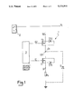
- FIG. 1 is a wiring diagram of the integrated circuit according to the invention.
- FIG. 2 is a side elevation cross-sectional view showing schematically the structure of the integrated circuit according to the invention.
- FIGS. 3 and 4 are respective side elevation cross-sectional views showing schematically modified embodiments of the circuit of FIGS. 1 and 2.
- circuit 1 which is self-protected against reversal of the polarity of a storage battery 2.
- the circuit 1 is expediently in the form of an integrated circuit.
- the circuit 1 comprises a first power transistor T1 of the DMOS type which is connected with its source electrode side to an electric load RL to drive said load toward ground.
- the transistor T1 has its source S1 connected to one end of said load RL which has the other end connected to ground.
- the circuit 1 further comprises a second, protective transistor T2, also of the DMOS type, which is connected between a positive pole Vc of the battery 2 and the first transistor T1.
- the source S2 of that transistor T2 is connected to said pole Vc, whereas the gate electrodes G1, G2 of the transistors T1, T2 are respectively connected to corresponding outputs of a circuit portion 3 driving the circuit 1.
- the respective drain regions D1 and D2 of the transistors T1 and T2 are shared in common and formed on a single polarity pod N (in the instance of an N-channel DMOS) in the semiconductor substrate with P polarity of that integrated structure.
- Each transistor includes, moreover, a corresponding intrinsic diode DT1 and DT2 which is connected in each transistor between the drain and the source and forward biased to the source. Furthermore, between the common drain D1, D2 of said transistors and the substrate there is provided a parasitic diode D forward biased to the substrate.
- the structure of the transistors T1 and T2 which are, in a preferred embodiment, a vertical high voltage (VDMOS) DMOS transistor and a lateral low voltage (LDMOS) DMOS transistor, interlaid with each other.
- VDMOS vertical high voltage
- LDMOS lateral low voltage
- a buried layer 9 doped oppositely from the substrate being in particular of the N+ type, which constitutes the low resistivity portion of said drain region D1-D2 shared by both of said transistors T1 and T2.
- the circuit of this invention is formed by alternating so-called source cells 8 of a vertical DMOS transistor T1 with source cells 8a of a lateral DMOS transistor T2, the latter having a lower specific series resistance than the former.
- High-doped N+ regions 5, also referred to as fingers, are provided which, by connecting the N+ buried layer 9 of the vertical DMOS to the surface in the proximities of the lateral DMOS fingers, form a low resistivity path for the flow of electrons which is picked up by the LDMOS from the VDMOS.
- the second transistor T2 Whenever the supply voltage Vc is applied, the second transistor T2 will be in conduction and protect the integrated circuit 1 in which the power actuator T1 is connected in all those cases when the polarity of the storage battery 2 has been reversed.
- the second transistor Upon the battery polarity being reversed, the second transistor will break and protect, therefore, both the driver and the load RL. This results because the drain-to-gate voltage of the second transistor T2 equals in negative value the voltage drop Vgs between the gate G2 and the source S2, so the second transistor T2 becomes operative as a Zener power diode protecting the integrated circuit 1.
- the voltage drop V across the second transistor can be made as small as desired by appropriate driving of the gate electrode, since that voltage is the product of the inherent resistance of the transistor T2 by the load current I1 flown therethrough.
- the resistance can be made quite small by increasing the surface area occupied by the transistor and correspondingly reducing the voltage drop thereacross as well as the dissipation of electric power.
- a vertical DMOS transistor with a lateral DMOS transistor respectively for a high and low voltage, enables the circuit to adequately withstand both reversals of the battery polarity, which would in all cases have a low voltage value in the 12-24 Volts range, and any dumping operational conditions apt to induce voltage peaks as high as 60 Volts.
- a further benefit is that the circuit of this invention can maximize the performance of the transistors incorporated thereto, especially in terms of the overall resistive drop, thereby the silicon surface area required for integration can be minimized.
- the drain regions are formed in the same pod or region, and accordingly, the two transistors do not require to be isolated on separate pods and waste useful area.
- This variant is particularly useful where the circuit 1 is not required to withstand dumping operational conditions.
- the circuit 1 comprises a pair of interlaid low voltage lateral transistors T10 and T11 of the DMOS type.
- the circuit 1 may be constructed by associating a pair of lateral DMOS transistors having gate regions with several extensions which serve substantially field plate functions.
- the gate electrode made of polycrystalline silicon can be extended and spread over the field oxide to provide a lateral DMOS transistor adapted to withstand high voltages.
- a lateral DMOS transistor can be obtained for low voltages.
- a high-doped zone 17 of the N+ type is introduced by ion implantation which is self-aligned to the field oxide on the side of the low voltage LDMOS transistor.
- circuit of the above-discussed variants operates in the same manner as the embodiment described first, to substantially bring about the same advantages.
Abstract
An integrated circuit self-protected against a reversal of its supply battery polarity comprises a first DMOS power transistor connected with its source electrode side to an electric load to be driven toward ground, and a second, protective DMOS transistor which is connected with its source electrode side to a positive pole of the battery and with its drain electrode side to the drain electrode of the first transistor. The first and second transistors have in common the drain region formed on a single pod in the semiconductor substrate.
Description
This invention relates to an integrated circuit self-protected against reversal of the supply battery polarity.
As is well known, on car assembly lines, the storage battery for the car electric system is customarily installed in each car toward the end of the assembly and installation steps of the electric system and utilities connected thereto.
The several electric loads represented by lights, actuators, and the like items, are usually driven between a positive supply pole and ground, with the intermediary of an electronic control circuit.
Since it may occur that the power supply cables to such electronic circuits in the system are inverted accidentally, there exists a need to accept fortuitous reversal of the installed battery polarity without said integrated circuits coming to any harm.
This demand also arises from a likelihood of errors occurring in the battery hook-up, and is intensified especially where the electric system includes power actuators for which no resistive components can be connected in the supply because such components are apt to bring down the supply voltage on account of the voltage drop thereacross.
To meet this demand, the prior art has proposed that a one-way component, specifically a diode, be used which is connected externally between the electronic control circuit and the positive supply pole to protect said integrated circuit in the event of the battery polarity being reversed.
While being advantageous cost-wise, this prior approach has drawbacks in that the voltage drop Vd across the diode brings down the voltage available to the electric load to be driven; in addition, the system efficiency deteriorates because the dissipated power is increased by an amount equal to the voltage VD on the diode multiplied by the current I1 that flows through the load.
The technical problem underlying this invention is to provide an integrated circuit which has such structural and performance characteristics as to obviate the cited drawbacks with which the prior art is beset.
This problem is solved by a circuit as indicated comprising:
a first DMOS power transistor connected with its source electrode side to an electric load to be driven toward ground;
a second, protective DMOS transistor connected with its source electrode side to a positive pole of the battery, and with its drain electrode side to the drain electrode of said first transistor;
said first and second transistors having the drain region in common.
The features and advantages of a circuit according to the invention will become more clearly apparent from the following detailed description of an embodiment thereof, given by way of example and not of limitation with reference to the accompanying drawings.
In the drawings:
FIG. 1 is a wiring diagram of the integrated circuit according to the invention;
FIG. 2 is a side elevation cross-sectional view showing schematically the structure of the integrated circuit according to the invention; and
FIGS. 3 and 4 are respective side elevation cross-sectional views showing schematically modified embodiments of the circuit of FIGS. 1 and 2.
With reference to the drawing views, generally and schematically shown at 1 is a circuit which is self-protected against reversal of the polarity of a storage battery 2. The circuit 1 is expediently in the form of an integrated circuit.
The circuit 1 comprises a first power transistor T1 of the DMOS type which is connected with its source electrode side to an electric load RL to drive said load toward ground.
More specifically, the transistor T1 has its source S1 connected to one end of said load RL which has the other end connected to ground.
The circuit 1 further comprises a second, protective transistor T2, also of the DMOS type, which is connected between a positive pole Vc of the battery 2 and the first transistor T1. The source S2 of that transistor T2 is connected to said pole Vc, whereas the gate electrodes G1, G2 of the transistors T1, T2 are respectively connected to corresponding outputs of a circuit portion 3 driving the circuit 1.
Advantageously, the respective drain regions D1 and D2 of the transistors T1 and T2 are shared in common and formed on a single polarity pod N (in the instance of an N-channel DMOS) in the semiconductor substrate with P polarity of that integrated structure.
Each transistor includes, moreover, a corresponding intrinsic diode DT1 and DT2 which is connected in each transistor between the drain and the source and forward biased to the source. Furthermore, between the common drain D1, D2 of said transistors and the substrate there is provided a parasitic diode D forward biased to the substrate.
More specifically, there is shown in the example according to FIG. 2 the structure of the transistors T1 and T2 which are, in a preferred embodiment, a vertical high voltage (VDMOS) DMOS transistor and a lateral low voltage (LDMOS) DMOS transistor, interlaid with each other.
It may be appreciated from FIG. 2 that in a semiconductor substrate 4 slightly doped with P-type impurities, there is formed a buried layer 9 doped oppositely from the substrate, being in particular of the N+ type, which constitutes the low resistivity portion of said drain region D1-D2 shared by both of said transistors T1 and T2.
Over the epitaxially grown, buried layer 9, there are formed the transistor common drain D1, D2 regions 6 and 7 being doped N- alike but with a lower dopant concentration than the buried layer 9, in which conventional zones 8 and 8a, also referred to as source cells, are formed.
Thus, the circuit of this invention is formed by alternating so-called source cells 8 of a vertical DMOS transistor T1 with source cells 8a of a lateral DMOS transistor T2, the latter having a lower specific series resistance than the former.
High-doped N+ regions 5, also referred to as fingers, are provided which, by connecting the N+ buried layer 9 of the vertical DMOS to the surface in the proximities of the lateral DMOS fingers, form a low resistivity path for the flow of electrons which is picked up by the LDMOS from the VDMOS.
Whenever the supply voltage Vc is applied, the second transistor T2 will be in conduction and protect the integrated circuit 1 in which the power actuator T1 is connected in all those cases when the polarity of the storage battery 2 has been reversed.
With the device driver 3 in operation, a current I1 is flown through the load RL which is supplied from the first transistor T1 via the second, protection transistor T2.
Upon the battery polarity being reversed, the second transistor will break and protect, therefore, both the driver and the load RL. This results because the drain-to-gate voltage of the second transistor T2 equals in negative value the voltage drop Vgs between the gate G2 and the source S2, so the second transistor T2 becomes operative as a Zener power diode protecting the integrated circuit 1.
Advantageously, the voltage drop V across the second transistor can be made as small as desired by appropriate driving of the gate electrode, since that voltage is the product of the inherent resistance of the transistor T2 by the load current I1 flown therethrough. In view of the value of that resistance being inversely proportional to the silicon surface area occupied by the second transistor in the integrated circuit 1, the resistance can be made quite small by increasing the surface area occupied by the transistor and correspondingly reducing the voltage drop thereacross as well as the dissipation of electric power.
Furthermore, the combination of a vertical DMOS transistor with a lateral DMOS transistor, respectively for a high and low voltage, enables the circuit to adequately withstand both reversals of the battery polarity, which would in all cases have a low voltage value in the 12-24 Volts range, and any dumping operational conditions apt to induce voltage peaks as high as 60 Volts.
A further benefit is that the circuit of this invention can maximize the performance of the transistors incorporated thereto, especially in terms of the overall resistive drop, thereby the silicon surface area required for integration can be minimized. The drain regions are formed in the same pod or region, and accordingly, the two transistors do not require to be isolated on separate pods and waste useful area.
With specific reference to the example shown in FIG. 3, a modified embodiment of the inventive circuit will be now described in which cooperating items and parts which are structured and operate similarly to the preceding embodiment are designated by the same reference numerals.
This variant is particularly useful where the circuit 1 is not required to withstand dumping operational conditions.
In this variant, the circuit 1 comprises a pair of interlaid low voltage lateral transistors T10 and T11 of the DMOS type.
More specifically, in a semiconductor substrate 4 which is P-doped slightly, there is provided a buried layer 9 doped N+ oppositely from the substrate, which bounds, in cooperation with opposing lateral regions 12 and 13 having a higher concentration of the same P-type dopant as the substrate, a pod 14 doped N- which is adapted to form the drain region shared by both transistors T10 and T11 in common.
Formed on said pod 14 are also conventional source regions 15 alternating with gates 16 as is typical of the structure of lateral DMOS transistors.
In a further modified embodiment, as shown in FIG. 4, the circuit 1 may be constructed by associating a pair of lateral DMOS transistors having gate regions with several extensions which serve substantially field plate functions. Using the planos technique, in fact, the gate electrode made of polycrystalline silicon can be extended and spread over the field oxide to provide a lateral DMOS transistor adapted to withstand high voltages. Conversely, by reducing the spread of the gate electrode over the field oxide, a lateral DMOS transistor can be obtained for low voltages.
Furthermore, to reduce the resistive path between adjacent sources, using the locos technique to provide the field oxide, a high-doped zone 17 of the N+ type is introduced by ion implantation which is self-aligned to the field oxide on the side of the low voltage LDMOS transistor.
The circuit of the above-discussed variants operates in the same manner as the embodiment described first, to substantially bring about the same advantages.
Claims (9)
1. An integrated circuit self-protected against a reversal of its supply battery polarity, characterized in that it comprises a first DMOS power transistor connected with its source electrode side to an electric load to be driven toward ground, and a second, protective DMOS transistor connected with its source electrode side to a positive pole of the battery and with its drain electrode side to the drain electrode of said first transistor, said first and second transistors having the drain region in common.
2. A circuit according to claim 1, characterized in that said first transistor is a DMOS transistor of the vertical type.
3. A circuit according to claim 1, characterized in that said first transistor is a high voltage lateral DMOS transistor.
4. A circuit according to claim 2, characterized in that said second transistor is a lateral DMOS transistor.
5. A circuit according to claim 4, characterized in that the integrated circuit comprises at least one region of N+ polarity fingers between said vertical DMOS transistor and said second lateral DMOS transistor in the common drain region to lower the circuit specific series resistance.
6. A circuit according to claim 4, characterized in that the integrated circuit comprises at least one N+ doped region self-aligned to a field oxide on the side of said second lateral DMOS transistor to lower the circuit specific series resistance.
7. An integrated circuit self-protected against a reversal of its supply battery polarity, comprising a first MOS power transistor having source and drain electrodes, and a second protective MOS transistor having source and drain electrodes, means for connecting the first transistor source electrode to an electrical load connected to ground, means for connecting the second transistor source electrode to a pole of the battery, means for connecting the second transistor drain electrode to the first transistor drain electrode, said first and second transistors being located in the same semiconductor substrate.
8. A circuit according to claim 7, wherein said first transistor is a DMOS vertical transistor, said second transistor is a DMOS lateral transistor, and the first and second transistor drain electrodes share a common region of the substrate.
9. A circuit according to claim 7, further comprising means to lower the specific series resistance of the second transistor.
Applications Claiming Priority (2)
| Application Number | Priority Date | Filing Date | Title |
|---|---|---|---|
| IT8822085A IT1227104B (en) | 1988-09-27 | 1988-09-27 | SELF-PROTECTED INTEGRATED CIRCUIT FROM POLARITY INVERSIONS OF THE POWER BATTERY |
| IT22085A/88 | 1988-09-27 |
Publications (1)
| Publication Number | Publication Date |
|---|---|
| US5126911A true US5126911A (en) | 1992-06-30 |
Family
ID=11191276
Family Applications (1)
| Application Number | Title | Priority Date | Filing Date |
|---|---|---|---|
| US07/385,721 Expired - Lifetime US5126911A (en) | 1988-09-27 | 1989-07-26 | Integrated circuit self-protected against reversal of the supply battery polarity |
Country Status (5)
| Country | Link |
|---|---|
| US (1) | US5126911A (en) |
| EP (1) | EP0360991B1 (en) |
| JP (1) | JP2905227B2 (en) |
| DE (1) | DE68917839T2 (en) |
| IT (1) | IT1227104B (en) |
Cited By (21)
| Publication number | Priority date | Publication date | Assignee | Title |
|---|---|---|---|---|
| US5434739A (en) * | 1993-06-14 | 1995-07-18 | Motorola, Inc. | Reverse battery protection circuit |
| US5648739A (en) * | 1994-09-16 | 1997-07-15 | Robert Bosch Gmbh | Switching device having a polarity reversal protection system |
| US5939863A (en) * | 1997-01-31 | 1999-08-17 | International Rectifier Corp. | Power circuit providing reverse battery protection and current and temperature sensing |
| US6278154B1 (en) * | 1996-11-08 | 2001-08-21 | Sony Corporation | Semiconductor apparatus and solid state imaging device |
| US6304422B1 (en) * | 1998-04-21 | 2001-10-16 | Infineon Technologies Ag | Polarity reversal protection circuit |
| US6353345B1 (en) * | 2000-04-04 | 2002-03-05 | Philips Electronics North America Corporation | Low cost half bridge driver integrated circuit with capability of using high threshold voltage DMOS |
| US6529356B2 (en) * | 2000-11-14 | 2003-03-04 | Silicon Touch Technology Inc. | Power polarity reversal protecting circuit for an integrated circuit |
| US6556400B1 (en) * | 1999-08-13 | 2003-04-29 | Micronas Gmbh | Reverse polarity protection circuit |
| US6611410B1 (en) | 1999-12-17 | 2003-08-26 | Siemens Vdo Automotive Inc. | Positive supply lead reverse polarity protection circuit |
| US6650520B2 (en) * | 2001-10-26 | 2003-11-18 | Koninklijke Philips Electronics N.V. | Power supply reverse bias protection circuit for protecting both analog and digital devices coupled thereto |
| US20040109272A1 (en) * | 2002-12-06 | 2004-06-10 | Phichej Cheevanantachai | Power converter with polarity reversal and inrush current protection circuit |
| US20040119116A1 (en) * | 2002-07-26 | 2004-06-24 | Jae-Il Byeon | Array of pull-up transistors for high voltage output circuit |
| US6781804B1 (en) * | 1997-06-17 | 2004-08-24 | Sgs-Thomson Microelectronics S.A. | Protection of the logic well of a component including an integrated MOS power transistor |
| US20050017690A1 (en) * | 2002-07-17 | 2005-01-27 | Mathews Associates, Inc. | Battery heating circuit |
| US20060012342A1 (en) * | 2002-07-17 | 2006-01-19 | Mathews Associates, Inc. | Self-heating battery that automatically adjusts its heat setting |
| US20100014201A1 (en) * | 2006-11-10 | 2010-01-21 | E2V Semiconductors | Logic output stage of integrated circuit protected against battery inversion |
| US20140103990A1 (en) * | 2012-10-12 | 2014-04-17 | The Boeing Company | Fault Tolerant Fail-Safe Link |
| US9559681B2 (en) | 2014-01-31 | 2017-01-31 | Alps Electric Co., Ltd. | Semiconductor integrated circuit device |
| US10250255B2 (en) | 2015-04-16 | 2019-04-02 | Renesas Electronics Corporation | Semiconductor device and circuit arrangement using the same |
| US10522675B2 (en) | 2012-01-25 | 2019-12-31 | Infineon Technologies Ag | Integrated circuit including field effect transistor structures with gate and field electrodes and methods for manufacturing and operating an integrated circuit |
| US20230054739A1 (en) * | 2019-12-26 | 2023-02-23 | Autonetworks Technologies, Ltd. | Power supply control device |
Families Citing this family (7)
| Publication number | Priority date | Publication date | Assignee | Title |
|---|---|---|---|---|
| US5151767A (en) * | 1991-05-03 | 1992-09-29 | North American Philips Corp. | Power integrated circuit having reverse-voltage protection |
| DE4137452A1 (en) * | 1991-11-14 | 1993-05-19 | Bosch Gmbh Robert | POLE PROTECTION ARRANGEMENT FOR POWER AMPLIFIER FIELD EFFECT TRANSISTORS |
| EP0561451B1 (en) * | 1992-03-16 | 1998-08-12 | Koninklijke Philips Electronics N.V. | Integrated semiconductor circuit including protection means |
| JP3216743B2 (en) * | 1993-04-22 | 2001-10-09 | 富士電機株式会社 | Protection diode for transistor |
| JP3485655B2 (en) * | 1994-12-14 | 2004-01-13 | 株式会社ルネサステクノロジ | Composite MOSFET |
| DE19509024C1 (en) * | 1995-03-13 | 1996-10-31 | Sgs Thomson Microelectronics | Integrated semiconductor circuit (controllable semiconductor switch) with protection against negative potential |
| JP2008244487A (en) * | 2008-04-21 | 2008-10-09 | Renesas Technology Corp | Compound type mosfet |
Citations (11)
| Publication number | Priority date | Publication date | Assignee | Title |
|---|---|---|---|---|
| US3712995A (en) * | 1972-03-27 | 1973-01-23 | Rca Corp | Input transient protection for complementary insulated gate field effect transistor integrated circuit device |
| US3829709A (en) * | 1973-08-31 | 1974-08-13 | Micro Components Corp | Supply reversal protecton circuit |
| US3940785A (en) * | 1974-05-06 | 1976-02-24 | Sprague Electric Company | Semiconductor I.C. with protection against reversed power supply |
| DE3133518A1 (en) * | 1981-08-25 | 1983-03-17 | Licentia Patent-Verwaltungs-Gmbh, 6000 Frankfurt | Electronic switch |
| US4423456A (en) * | 1981-11-13 | 1983-12-27 | Medtronic, Inc. | Battery reversal protection |
| US4589004A (en) * | 1981-03-30 | 1986-05-13 | Tokyo Shibaura Denki Kabushiki Kaisha | Semiconductor device monolithically comprising a V-MOSFET and bipolar transistor isolated from each other |
| US4698582A (en) * | 1986-07-23 | 1987-10-06 | Motorola, Inc. | Power driver having short circuit protection |
| JPS63219153A (en) * | 1987-03-06 | 1988-09-12 | Matsushita Electronics Corp | Semiconductor integrated circuit |
| US4858055A (en) * | 1987-07-23 | 1989-08-15 | Mitsubishi Denki Kabushiki Kaisha | Input protecting device for a semiconductor circuit device |
| US4958251A (en) * | 1988-07-05 | 1990-09-18 | Sgs-Thomson Microelectronics S.R.L. | Guarded electronic circuit from reversal of its supply battery polarity |
| US5027250A (en) * | 1988-07-05 | 1991-06-25 | Sgs-Thomson Microelectronics S.R.L. | Electronic circuit with a protection device against fluctuations in the supply battery voltage |
-
1988
- 1988-09-27 IT IT8822085A patent/IT1227104B/en active
-
1989
- 1989-07-12 DE DE68917839T patent/DE68917839T2/en not_active Expired - Fee Related
- 1989-07-12 EP EP89112711A patent/EP0360991B1/en not_active Expired - Lifetime
- 1989-07-26 US US07/385,721 patent/US5126911A/en not_active Expired - Lifetime
- 1989-09-13 JP JP1235840A patent/JP2905227B2/en not_active Expired - Lifetime
Patent Citations (11)
| Publication number | Priority date | Publication date | Assignee | Title |
|---|---|---|---|---|
| US3712995A (en) * | 1972-03-27 | 1973-01-23 | Rca Corp | Input transient protection for complementary insulated gate field effect transistor integrated circuit device |
| US3829709A (en) * | 1973-08-31 | 1974-08-13 | Micro Components Corp | Supply reversal protecton circuit |
| US3940785A (en) * | 1974-05-06 | 1976-02-24 | Sprague Electric Company | Semiconductor I.C. with protection against reversed power supply |
| US4589004A (en) * | 1981-03-30 | 1986-05-13 | Tokyo Shibaura Denki Kabushiki Kaisha | Semiconductor device monolithically comprising a V-MOSFET and bipolar transistor isolated from each other |
| DE3133518A1 (en) * | 1981-08-25 | 1983-03-17 | Licentia Patent-Verwaltungs-Gmbh, 6000 Frankfurt | Electronic switch |
| US4423456A (en) * | 1981-11-13 | 1983-12-27 | Medtronic, Inc. | Battery reversal protection |
| US4698582A (en) * | 1986-07-23 | 1987-10-06 | Motorola, Inc. | Power driver having short circuit protection |
| JPS63219153A (en) * | 1987-03-06 | 1988-09-12 | Matsushita Electronics Corp | Semiconductor integrated circuit |
| US4858055A (en) * | 1987-07-23 | 1989-08-15 | Mitsubishi Denki Kabushiki Kaisha | Input protecting device for a semiconductor circuit device |
| US4958251A (en) * | 1988-07-05 | 1990-09-18 | Sgs-Thomson Microelectronics S.R.L. | Guarded electronic circuit from reversal of its supply battery polarity |
| US5027250A (en) * | 1988-07-05 | 1991-06-25 | Sgs-Thomson Microelectronics S.R.L. | Electronic circuit with a protection device against fluctuations in the supply battery voltage |
Non-Patent Citations (2)
| Title |
|---|
| Patent Abstracts of Japan vol. 13, No. 8 (E 702) (3356) Jan. 10, 1989 & JP-A-63 219153 (MATSUSHITA) 12 September 1988 * |
| Patent Abstracts of Japan vol. 13, No. 8 (E-702) (3356) Jan. 10, 1989. |
Cited By (27)
| Publication number | Priority date | Publication date | Assignee | Title |
|---|---|---|---|---|
| US5434739A (en) * | 1993-06-14 | 1995-07-18 | Motorola, Inc. | Reverse battery protection circuit |
| US5648739A (en) * | 1994-09-16 | 1997-07-15 | Robert Bosch Gmbh | Switching device having a polarity reversal protection system |
| US6278154B1 (en) * | 1996-11-08 | 2001-08-21 | Sony Corporation | Semiconductor apparatus and solid state imaging device |
| US5939863A (en) * | 1997-01-31 | 1999-08-17 | International Rectifier Corp. | Power circuit providing reverse battery protection and current and temperature sensing |
| US6781804B1 (en) * | 1997-06-17 | 2004-08-24 | Sgs-Thomson Microelectronics S.A. | Protection of the logic well of a component including an integrated MOS power transistor |
| US6304422B1 (en) * | 1998-04-21 | 2001-10-16 | Infineon Technologies Ag | Polarity reversal protection circuit |
| US6556400B1 (en) * | 1999-08-13 | 2003-04-29 | Micronas Gmbh | Reverse polarity protection circuit |
| US6611410B1 (en) | 1999-12-17 | 2003-08-26 | Siemens Vdo Automotive Inc. | Positive supply lead reverse polarity protection circuit |
| US6353345B1 (en) * | 2000-04-04 | 2002-03-05 | Philips Electronics North America Corporation | Low cost half bridge driver integrated circuit with capability of using high threshold voltage DMOS |
| US6529356B2 (en) * | 2000-11-14 | 2003-03-04 | Silicon Touch Technology Inc. | Power polarity reversal protecting circuit for an integrated circuit |
| US6650520B2 (en) * | 2001-10-26 | 2003-11-18 | Koninklijke Philips Electronics N.V. | Power supply reverse bias protection circuit for protecting both analog and digital devices coupled thereto |
| US20050017690A1 (en) * | 2002-07-17 | 2005-01-27 | Mathews Associates, Inc. | Battery heating circuit |
| US20060012342A1 (en) * | 2002-07-17 | 2006-01-19 | Mathews Associates, Inc. | Self-heating battery that automatically adjusts its heat setting |
| US7327122B2 (en) | 2002-07-17 | 2008-02-05 | Mathews Associates, Inc. | Battery heating circuit |
| US20040119116A1 (en) * | 2002-07-26 | 2004-06-24 | Jae-Il Byeon | Array of pull-up transistors for high voltage output circuit |
| US7190025B2 (en) * | 2002-07-26 | 2007-03-13 | Samsung Electronics Co., Ltd. | Array of pull-up transistors for high voltage output circuit |
| US20040109272A1 (en) * | 2002-12-06 | 2004-06-10 | Phichej Cheevanantachai | Power converter with polarity reversal and inrush current protection circuit |
| US7012793B2 (en) * | 2002-12-06 | 2006-03-14 | Delta Electronics, Inc. | Power converter with polarity reversal and inrush current protection circuit |
| US20100014201A1 (en) * | 2006-11-10 | 2010-01-21 | E2V Semiconductors | Logic output stage of integrated circuit protected against battery inversion |
| US10522675B2 (en) | 2012-01-25 | 2019-12-31 | Infineon Technologies Ag | Integrated circuit including field effect transistor structures with gate and field electrodes and methods for manufacturing and operating an integrated circuit |
| DE102013100683B4 (en) * | 2012-01-25 | 2021-03-11 | Infineon Technologies Ag | Integrated circuit with field effect transistor structures with gate and field electrodes and method for producing such an integrated circuit |
| US20140103990A1 (en) * | 2012-10-12 | 2014-04-17 | The Boeing Company | Fault Tolerant Fail-Safe Link |
| US8891218B2 (en) * | 2012-10-12 | 2014-11-18 | The Boeing Company | Fault tolerant fail-safe link |
| US9559681B2 (en) | 2014-01-31 | 2017-01-31 | Alps Electric Co., Ltd. | Semiconductor integrated circuit device |
| US10250255B2 (en) | 2015-04-16 | 2019-04-02 | Renesas Electronics Corporation | Semiconductor device and circuit arrangement using the same |
| US20230054739A1 (en) * | 2019-12-26 | 2023-02-23 | Autonetworks Technologies, Ltd. | Power supply control device |
| US11870427B2 (en) * | 2019-12-26 | 2024-01-09 | Autonetworks Technologies, Ltd. | Power supply control device |
Also Published As
| Publication number | Publication date |
|---|---|
| DE68917839D1 (en) | 1994-10-06 |
| JP2905227B2 (en) | 1999-06-14 |
| IT1227104B (en) | 1991-03-15 |
| IT8822085A0 (en) | 1988-09-27 |
| EP0360991B1 (en) | 1994-08-31 |
| EP0360991A2 (en) | 1990-04-04 |
| EP0360991A3 (en) | 1991-03-20 |
| JPH02122665A (en) | 1990-05-10 |
| DE68917839T2 (en) | 1994-12-22 |
Similar Documents
| Publication | Publication Date | Title |
|---|---|---|
| US5126911A (en) | Integrated circuit self-protected against reversal of the supply battery polarity | |
| US9912329B2 (en) | Semiconductor device and driving system | |
| EP0505191B1 (en) | Semiconductor device with low concentration n region to improve dV/dt capability | |
| US9960156B2 (en) | Integrated semiconductor device having a level shifter | |
| EP0562271B1 (en) | High voltage structure with oxide isolated source and resurf drift region in bulk silicon | |
| EP0305937B1 (en) | Mos i/o protection using switched body circuit design | |
| US6380566B1 (en) | Semiconductor device having FET structure with high breakdown voltage | |
| US20050167753A1 (en) | Insulated gate bipolar transistor and electrostatic discharge cell protection utilizing insulated gate bipolar tansistors | |
| US20050139958A1 (en) | Thick gate oxide transistor and electrostatic discharge protection utilizing thick gate oxide transistors | |
| US7279773B2 (en) | Protection device for handling energy transients | |
| US8022477B2 (en) | Semiconductor apparatus having lateral type MIS transistor | |
| KR100922914B1 (en) | Field effect transistor formed on an insulating substrate | |
| US20210143148A1 (en) | Semiconductor device | |
| US10547304B2 (en) | Semiconductor integrated circuit for driving switching device with integrated negative voltage clamp diode | |
| US5313088A (en) | Vertical field effect transistor with diffused protection diode | |
| US6778366B2 (en) | Current limiting protection circuit | |
| US11948937B2 (en) | Semiconductor integrated circuit with edge structure to decrease leakage current | |
| US10199452B2 (en) | Semiconductor device | |
| US5466952A (en) | Semiconductor device having an IGET and a control or protection component | |
| EP1139566B1 (en) | Semiconductor circuit with insulated gate device and associated control circuitry | |
| US7470955B2 (en) | Technique for improving negative potential immunity of an integrated circuit | |
| US6781804B1 (en) | Protection of the logic well of a component including an integrated MOS power transistor | |
| US20230361109A1 (en) | Protection circuit and semiconductor integrated circuit device | |
| JPH0430571A (en) | Semiconductor integrated circuit for high dielectric strength type drive | |
| JPH04321773A (en) | Power integrated circuit for automobile |
Legal Events
| Date | Code | Title | Description |
|---|---|---|---|
| AS | Assignment |
Owner name: SGS-THOMSON MICROELECTRONICS S.R.L., VIA C. OLIVET Free format text: ASSIGNMENT OF ASSIGNORS INTEREST.;ASSIGNORS:CONTIERO, CLAUDIO;MURARI, BRUNO;REEL/FRAME:005104/0946 Effective date: 19890630 |
|
| STCF | Information on status: patent grant |
Free format text: PATENTED CASE |
|
| FPAY | Fee payment |
Year of fee payment: 4 |
|
| FPAY | Fee payment |
Year of fee payment: 8 |
|
| FPAY | Fee payment |
Year of fee payment: 12 |