US5124717A - Ink jet printhead having integral filter - Google Patents
Ink jet printhead having integral filter Download PDFInfo
- Publication number
- US5124717A US5124717A US07/624,390 US62439090A US5124717A US 5124717 A US5124717 A US 5124717A US 62439090 A US62439090 A US 62439090A US 5124717 A US5124717 A US 5124717A
- Authority
- US
- United States
- Prior art keywords
- layer
- printhead
- filter
- manifold
- ink
- Prior art date
- Legal status (The legal status is an assumption and is not a legal conclusion. Google has not performed a legal analysis and makes no representation as to the accuracy of the status listed.)
- Expired - Fee Related
Links
- 239000012528 membrane Substances 0.000 claims abstract description 29
- 239000011148 porous material Substances 0.000 claims abstract description 25
- 230000013011 mating Effects 0.000 claims abstract description 3
- 239000000758 substrate Substances 0.000 claims description 41
- 229910052581 Si3N4 Inorganic materials 0.000 claims description 37
- HQVNEWCFYHHQES-UHFFFAOYSA-N silicon nitride Chemical compound N12[Si]34N5[Si]62N3[Si]51N64 HQVNEWCFYHHQES-UHFFFAOYSA-N 0.000 claims description 37
- 238000010438 heat treatment Methods 0.000 claims description 24
- XUIMIQQOPSSXEZ-UHFFFAOYSA-N Silicon Chemical compound [Si] XUIMIQQOPSSXEZ-UHFFFAOYSA-N 0.000 claims description 20
- 239000010703 silicon Substances 0.000 claims description 20
- 229910052710 silicon Inorganic materials 0.000 claims description 20
- 238000004519 manufacturing process Methods 0.000 claims description 15
- 238000000034 method Methods 0.000 claims description 13
- 238000005530 etching Methods 0.000 claims description 12
- 238000000151 deposition Methods 0.000 claims description 11
- 239000000463 material Substances 0.000 claims description 9
- 238000004891 communication Methods 0.000 claims description 7
- 229920002120 photoresistant polymer Polymers 0.000 claims description 7
- 239000002019 doping agent Substances 0.000 claims description 3
- 230000005499 meniscus Effects 0.000 claims description 3
- 239000002245 particle Substances 0.000 claims description 3
- 238000000059 patterning Methods 0.000 claims 4
- 230000008021 deposition Effects 0.000 claims 3
- 238000009434 installation Methods 0.000 claims 2
- 235000012431 wafers Nutrition 0.000 abstract description 41
- 230000000873 masking effect Effects 0.000 abstract description 3
- 239000010410 layer Substances 0.000 description 51
- 238000011109 contamination Methods 0.000 description 5
- 229910052751 metal Inorganic materials 0.000 description 5
- 239000002184 metal Substances 0.000 description 5
- 239000004642 Polyimide Substances 0.000 description 4
- 239000010408 film Substances 0.000 description 4
- 238000001914 filtration Methods 0.000 description 4
- 229920001721 polyimide Polymers 0.000 description 4
- 239000004065 semiconductor Substances 0.000 description 4
- 239000002344 surface layer Substances 0.000 description 4
- 230000032798 delamination Effects 0.000 description 3
- 239000012530 fluid Substances 0.000 description 3
- 238000010030 laminating Methods 0.000 description 3
- 150000004767 nitrides Chemical class 0.000 description 3
- 238000001020 plasma etching Methods 0.000 description 3
- 238000007639 printing Methods 0.000 description 3
- ZOXJGFHDIHLPTG-UHFFFAOYSA-N Boron Chemical compound [B] ZOXJGFHDIHLPTG-UHFFFAOYSA-N 0.000 description 2
- NHWNVPNZGGXQQV-UHFFFAOYSA-J [Si+4].[O-]N=O.[O-]N=O.[O-]N=O.[O-]N=O Chemical compound [Si+4].[O-]N=O.[O-]N=O.[O-]N=O.[O-]N=O NHWNVPNZGGXQQV-UHFFFAOYSA-J 0.000 description 2
- 230000005540 biological transmission Effects 0.000 description 2
- 229910052796 boron Inorganic materials 0.000 description 2
- 241001379910 Ephemera danica Species 0.000 description 1
- 239000004593 Epoxy Substances 0.000 description 1
- PXGOKWXKJXAPGV-UHFFFAOYSA-N Fluorine Chemical compound FF PXGOKWXKJXAPGV-UHFFFAOYSA-N 0.000 description 1
- KWYUFKZDYYNOTN-UHFFFAOYSA-M Potassium hydroxide Chemical compound [OH-].[K+] KWYUFKZDYYNOTN-UHFFFAOYSA-M 0.000 description 1
- QVGXLLKOCUKJST-UHFFFAOYSA-N atomic oxygen Chemical compound [O] QVGXLLKOCUKJST-UHFFFAOYSA-N 0.000 description 1
- BGTFCAQCKWKTRL-YDEUACAXSA-N chembl1095986 Chemical compound C1[C@@H](N)[C@@H](O)[C@H](C)O[C@H]1O[C@@H]([C@H]1C(N[C@H](C2=CC(O)=CC(O[C@@H]3[C@H]([C@@H](O)[C@H](O)[C@@H](CO)O3)O)=C2C=2C(O)=CC=C(C=2)[C@@H](NC(=O)[C@@H]2NC(=O)[C@@H]3C=4C=C(C(=C(O)C=4)C)OC=4C(O)=CC=C(C=4)[C@@H](N)C(=O)N[C@@H](C(=O)N3)[C@H](O)C=3C=CC(O4)=CC=3)C(=O)N1)C(O)=O)=O)C(C=C1)=CC=C1OC1=C(O[C@@H]3[C@H]([C@H](O)[C@@H](O)[C@H](CO[C@@H]5[C@H]([C@@H](O)[C@H](O)[C@@H](C)O5)O)O3)O[C@@H]3[C@H]([C@@H](O)[C@H](O)[C@@H](CO)O3)O[C@@H]3[C@H]([C@H](O)[C@@H](CO)O3)O)C4=CC2=C1 BGTFCAQCKWKTRL-YDEUACAXSA-N 0.000 description 1
- 230000003749 cleanliness Effects 0.000 description 1
- 238000005520 cutting process Methods 0.000 description 1
- 238000009792 diffusion process Methods 0.000 description 1
- 238000010894 electron beam technology Methods 0.000 description 1
- 238000005516 engineering process Methods 0.000 description 1
- 229910052731 fluorine Inorganic materials 0.000 description 1
- 239000011737 fluorine Substances 0.000 description 1
- 238000007641 inkjet printing Methods 0.000 description 1
- 238000005468 ion implantation Methods 0.000 description 1
- 238000012986 modification Methods 0.000 description 1
- 230000004048 modification Effects 0.000 description 1
- 229910052760 oxygen Inorganic materials 0.000 description 1
- 239000001301 oxygen Substances 0.000 description 1
- 230000000149 penetrating effect Effects 0.000 description 1
- 230000035515 penetration Effects 0.000 description 1
- 239000005373 porous glass Substances 0.000 description 1
- 238000007789 sealing Methods 0.000 description 1
- 230000035945 sensitivity Effects 0.000 description 1
- 238000005728 strengthening Methods 0.000 description 1
- 238000007651 thermal printing Methods 0.000 description 1
- 239000010409 thin film Substances 0.000 description 1
- 238000010023 transfer printing Methods 0.000 description 1
- 238000011144 upstream manufacturing Methods 0.000 description 1
Images


Classifications
-
- B—PERFORMING OPERATIONS; TRANSPORTING
- B41—PRINTING; LINING MACHINES; TYPEWRITERS; STAMPS
- B41J—TYPEWRITERS; SELECTIVE PRINTING MECHANISMS, i.e. MECHANISMS PRINTING OTHERWISE THAN FROM A FORME; CORRECTION OF TYPOGRAPHICAL ERRORS
- B41J2/00—Typewriters or selective printing mechanisms characterised by the printing or marking process for which they are designed
- B41J2/005—Typewriters or selective printing mechanisms characterised by the printing or marking process for which they are designed characterised by bringing liquid or particles selectively into contact with a printing material
- B41J2/01—Ink jet
- B41J2/135—Nozzles
- B41J2/16—Production of nozzles
- B41J2/1601—Production of bubble jet print heads
- B41J2/1604—Production of bubble jet print heads of the edge shooter type
-
- B—PERFORMING OPERATIONS; TRANSPORTING
- B41—PRINTING; LINING MACHINES; TYPEWRITERS; STAMPS
- B41J—TYPEWRITERS; SELECTIVE PRINTING MECHANISMS, i.e. MECHANISMS PRINTING OTHERWISE THAN FROM A FORME; CORRECTION OF TYPOGRAPHICAL ERRORS
- B41J2/00—Typewriters or selective printing mechanisms characterised by the printing or marking process for which they are designed
- B41J2/005—Typewriters or selective printing mechanisms characterised by the printing or marking process for which they are designed characterised by bringing liquid or particles selectively into contact with a printing material
- B41J2/01—Ink jet
- B41J2/135—Nozzles
- B41J2/16—Production of nozzles
- B41J2/1621—Manufacturing processes
- B41J2/1623—Manufacturing processes bonding and adhesion
-
- B—PERFORMING OPERATIONS; TRANSPORTING
- B41—PRINTING; LINING MACHINES; TYPEWRITERS; STAMPS
- B41J—TYPEWRITERS; SELECTIVE PRINTING MECHANISMS, i.e. MECHANISMS PRINTING OTHERWISE THAN FROM A FORME; CORRECTION OF TYPOGRAPHICAL ERRORS
- B41J2/00—Typewriters or selective printing mechanisms characterised by the printing or marking process for which they are designed
- B41J2/005—Typewriters or selective printing mechanisms characterised by the printing or marking process for which they are designed characterised by bringing liquid or particles selectively into contact with a printing material
- B41J2/01—Ink jet
- B41J2/135—Nozzles
- B41J2/16—Production of nozzles
- B41J2/1621—Manufacturing processes
- B41J2/1626—Manufacturing processes etching
- B41J2/1628—Manufacturing processes etching dry etching
-
- B—PERFORMING OPERATIONS; TRANSPORTING
- B41—PRINTING; LINING MACHINES; TYPEWRITERS; STAMPS
- B41J—TYPEWRITERS; SELECTIVE PRINTING MECHANISMS, i.e. MECHANISMS PRINTING OTHERWISE THAN FROM A FORME; CORRECTION OF TYPOGRAPHICAL ERRORS
- B41J2/00—Typewriters or selective printing mechanisms characterised by the printing or marking process for which they are designed
- B41J2/005—Typewriters or selective printing mechanisms characterised by the printing or marking process for which they are designed characterised by bringing liquid or particles selectively into contact with a printing material
- B41J2/01—Ink jet
- B41J2/135—Nozzles
- B41J2/16—Production of nozzles
- B41J2/1621—Manufacturing processes
- B41J2/1626—Manufacturing processes etching
- B41J2/1629—Manufacturing processes etching wet etching
-
- B—PERFORMING OPERATIONS; TRANSPORTING
- B41—PRINTING; LINING MACHINES; TYPEWRITERS; STAMPS
- B41J—TYPEWRITERS; SELECTIVE PRINTING MECHANISMS, i.e. MECHANISMS PRINTING OTHERWISE THAN FROM A FORME; CORRECTION OF TYPOGRAPHICAL ERRORS
- B41J2/00—Typewriters or selective printing mechanisms characterised by the printing or marking process for which they are designed
- B41J2/005—Typewriters or selective printing mechanisms characterised by the printing or marking process for which they are designed characterised by bringing liquid or particles selectively into contact with a printing material
- B41J2/01—Ink jet
- B41J2/135—Nozzles
- B41J2/16—Production of nozzles
- B41J2/1621—Manufacturing processes
- B41J2/1631—Manufacturing processes photolithography
-
- B—PERFORMING OPERATIONS; TRANSPORTING
- B41—PRINTING; LINING MACHINES; TYPEWRITERS; STAMPS
- B41J—TYPEWRITERS; SELECTIVE PRINTING MECHANISMS, i.e. MECHANISMS PRINTING OTHERWISE THAN FROM A FORME; CORRECTION OF TYPOGRAPHICAL ERRORS
- B41J2/00—Typewriters or selective printing mechanisms characterised by the printing or marking process for which they are designed
- B41J2/005—Typewriters or selective printing mechanisms characterised by the printing or marking process for which they are designed characterised by bringing liquid or particles selectively into contact with a printing material
- B41J2/01—Ink jet
- B41J2/135—Nozzles
- B41J2/16—Production of nozzles
- B41J2/1621—Manufacturing processes
- B41J2/1632—Manufacturing processes machining
-
- B—PERFORMING OPERATIONS; TRANSPORTING
- B41—PRINTING; LINING MACHINES; TYPEWRITERS; STAMPS
- B41J—TYPEWRITERS; SELECTIVE PRINTING MECHANISMS, i.e. MECHANISMS PRINTING OTHERWISE THAN FROM A FORME; CORRECTION OF TYPOGRAPHICAL ERRORS
- B41J2/00—Typewriters or selective printing mechanisms characterised by the printing or marking process for which they are designed
- B41J2/005—Typewriters or selective printing mechanisms characterised by the printing or marking process for which they are designed characterised by bringing liquid or particles selectively into contact with a printing material
- B41J2/01—Ink jet
- B41J2/135—Nozzles
- B41J2/16—Production of nozzles
- B41J2/1621—Manufacturing processes
- B41J2/1635—Manufacturing processes dividing the wafer into individual chips
-
- B—PERFORMING OPERATIONS; TRANSPORTING
- B41—PRINTING; LINING MACHINES; TYPEWRITERS; STAMPS
- B41J—TYPEWRITERS; SELECTIVE PRINTING MECHANISMS, i.e. MECHANISMS PRINTING OTHERWISE THAN FROM A FORME; CORRECTION OF TYPOGRAPHICAL ERRORS
- B41J2/00—Typewriters or selective printing mechanisms characterised by the printing or marking process for which they are designed
- B41J2/005—Typewriters or selective printing mechanisms characterised by the printing or marking process for which they are designed characterised by bringing liquid or particles selectively into contact with a printing material
- B41J2/01—Ink jet
- B41J2/135—Nozzles
- B41J2/16—Production of nozzles
- B41J2/1621—Manufacturing processes
- B41J2/164—Manufacturing processes thin film formation
- B41J2/1642—Manufacturing processes thin film formation thin film formation by CVD [chemical vapor deposition]
-
- B—PERFORMING OPERATIONS; TRANSPORTING
- B41—PRINTING; LINING MACHINES; TYPEWRITERS; STAMPS
- B41J—TYPEWRITERS; SELECTIVE PRINTING MECHANISMS, i.e. MECHANISMS PRINTING OTHERWISE THAN FROM A FORME; CORRECTION OF TYPOGRAPHICAL ERRORS
- B41J2/00—Typewriters or selective printing mechanisms characterised by the printing or marking process for which they are designed
- B41J2/005—Typewriters or selective printing mechanisms characterised by the printing or marking process for which they are designed characterised by bringing liquid or particles selectively into contact with a printing material
- B41J2/01—Ink jet
- B41J2/135—Nozzles
- B41J2/14—Structure thereof only for on-demand ink jet heads
- B41J2002/14403—Structure thereof only for on-demand ink jet heads including a filter
Definitions
- This invention relates to drop-on-demand ink jet printheads and more particularly, to a thermal ink jet printhead having an integral membrane filter over its ink inlet and process for fabricating the printhead with such filter.
- a typical thermally actuated drop-on-demand ink jet printing system uses thermal energy pulses to produce vapor bubbles in an ink-filled channel that expels droplets from the channel orifices of the printing system's printhead.
- Such printheads have one or more ink-filled channels communicating at one end with a relatively small ink supply chamber and having an orifice at the opposite end, also referred to as the nozzle.
- a thermal energy generator usually a resistor, is located in the channels near the nozzle at a predetermined distance upstream therefrom. The resistors are individually addressed with a current pulse to momentarily vaporize the ink and form a bubble which expels an ink droplet.
- a meniscus is formed at each nozzle under a slight negative pressure to prevent ink from weeping therefrom.
- U.S. Pat. No. 4,589,952 to Behringer et al discloses a method of making trenches having substantially vertical sidewalls in a silicon substrate using a three-level mask comprising a thick photoresist layer, a silicon nitrite layer, and a thin photoresist layer. Openings are formed in the thin photoresist layer and silicon nitrite layer by reactive ion etching in CF 4 . The openings are continued through the thick photoresist by etching in an atmosphere containing oxygen. The exposed surface of the silicon substrate is then etched in a CF 4 atmosphere containing a low concentration of fluorine. Also disclosed is a method of making an electron beam transmissive mask wherein the openings are made using a three level mask and reactive ion etching of silicon using the etching technique of this invention.
- U.S. Pat. No. 4,419,182 to Westerberg et al discloses a method of fabricating screen lenses and aperture array plates wherein a round, flat polish 100 silicon wafer is oxidized and exposed to a pattern photolithographically. The silicon wafer is then indiffused with boron and isotropically etched to produce the predetermined pattern of holes comprising a filter.
- U.S. Pat. No. 4,561,789 to Saito discloses a thermal ink transfer printing system containing a thermal printing head comprised of a porous glass substrate which is covered with a polyimide thin film and consequently photoetched to produce a pattern of holes comprising an ink filter.
- U.S. Pat. No. 4,417,946 to Bohlen et al discloses a mask for structuring surface areas and a method of manufacture of such mask.
- the mask includes at least one metal layer with apertures which define the mask pattern and a semiconductive substrate for carrying the metal layer.
- a semiconductor substrate has through holes that correspond to the mask pattern.
- the through holes in the semiconductor substrate extend from the metal covered surface on the front to at least one tub shaped recess which extends from the other back surface into the semiconductor substrate. Holes are provided in a surface layer in the semiconductor substrate.
- the surface layer differs in its doping from the rest of the substrate and the holes which are provided in the surface layer have lateral dimensions larger than the apertures in the metal layer so that the metal layer protrudes over the surface layer.
- U.S. Pat. No. 4,639,748 to Drake et al discloses an ink jet printhead having an internal filtering system and fabricating process therefore.
- Each printhead is composed of two parts aligned and bonded together.
- One part contains a linear array of heating elements and addressing electrodes on one surface.
- the other part has a parallel array of elongated recesses for use as ink channels and a common ink supplying manifold recess in communication with the ink channels.
- the manifold recess contains an integral closed wall defining a chamber with an ink-fill hole.
- Small passageways are formed in the internal chamber walls to permit passage of ink therefrom into the manifold.
- Each of the passageways have smaller cross-sectional flow areas than the nozzles to filter the ink, while the total cross-sectional flow area of the passageways is larger than the total cross-sectional flow areas of the nozzles.
- U.S. Pat. No. 4,864,329 to Kneezel et al discloses a thermal ink jet printhead having a flat filter placed over the inlet thereof by a fabrication process which laminates a wafer size filter to the aligned and bonded wafers containing a plurality of printheads.
- the individual printheads are obtained by a sectioning operation, which cuts through the two or more bonded wafers and the filter.
- the filter may be a woven mesh screen or preferably an electroformed screen with predetermined pore size. Since the filter covers one entire side of the printhead, a relatively large contact area prevents delamination and enables convenient leak-free sealing.
- a plurality of ink jet printheads with integral membrane filters are fabricated from two (100) silicon wafers.
- a plurality of sets of heating elements and their individually addressing electrodes are formed on the surface of one of the wafers and a corresponding plurality of sets of parallel channel grooves, each channel groove set communicating with a recessed manifold, are formed in a surface of the other wafer.
- the two wafers are aligned and bonded together and individual printheads are obtained by a sectioning operation which cuts the mated wafers into a plurality of printheads.
- the integral membrane filter is formed on the channel wafer after it is anisotroically etched and prior to mating with the heater plate wafer.
- a photopatternable layer is deposited over the etch resistant masking layer and exposed, patterned and developed to establish the mesh filter.
- a side of the channel wafer not patterned and etched is heavily doped to increase the robustness of the membrane filter by functioning as an etch stop.
- This doped region beneath the patternable layer is then etched using the membrane filter as a mask to open the filter pores through the doped layer portion of the channel wafer.
- the membrane filter In addition to filtering contamination from the ink and ink supply system during printing, the membrane filter also keeps dirt and other contamination from entering the large ink inlets during printhead assembly.
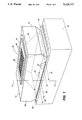
- FIG. 1 is a partially shown enlarged isometric view of a single printhead having the integral membrane filter of the present invention and showing the ink droplet emitting nozzles.
- FIG. 2 is a cross-sectional view of the printhead as viewed along view line 2--2 of FIG. 1.
- FIG. 3A-3F show partial cross-sectional views of the channel plate fabricating steps which include the fabrication of the integral membrane filter.
- FIGS. 4A-4E show partial cross-sectional views of the channel plate fabricating steps of an alternate embodiment of the present invention.
- a thermal ink jet printhead 10 of the present invention comprising channel plate 12 with integral membrane filter 14 and heater plate 16 shown in dashed line.
- a patterned film layer 18 is shown in dashed line having a material such as, for example, Riston®, Vacrel®, or polyimide, and is sandwiched between the channel plate and the heater plate.
- the thick film layer is etched to remove material above each heating element 34, thus placing them in pits 26, and to remove material between the closed ends 21 of ink channels 20 and the manifold 24 forming trench 38 in order to place the channels into fluid communication with the manifold.
- droplets 13 are shown following trajectories 15 after ejection from the nozzles 27 in front face 29 of the printhead.
- the printhead comprises a channel plate 12 that is permanently bonded to heater plate 16 or to the patterned thick film layer 18 optionally deposited over the heating elements and addressing electrodes on the top surface 19 of the heater plate and patterned as taught in the above-mentioned U.S. Pat. No. 4,774,530.
- the channel plate is silicon and the heater plate may be any insulative or semiconductive material as disclosed in the U.S. Pat. No. Re. 32,572 to Hawkins et al.
- the present invention is described for an edge-shooter type printhead, but could readily be used for a roofshooter configured printhead (not shown) as disclosed in U.S. Pat. No.
- Channel plate 12 of FIG. 1 contains an etched recess 24, shown in dashed line, in one surface which, when mated to the heater plate 16, forms an ink reservoir or manifold.
- a plurality of identical parallel grooves 20, shown in dashed line and having triangular cross sections, are etched in the same surface of the channel plate with one of the ends thereof penetrating the front face 29 thereof.
- the other closed ends 21 (FIG. 2) of the grooves are adjacent the recess 24.
- the groove penetrations through edge 29 produce the orifices or nozzles 27 and the grooves 20 serve as ink channels which connect the manifold with the nozzles.
- Filter 14 of the present invention has been fabricated, as discussed later, by depositing a photopatternable layer 23 over the etch resistant mask layer 22 and photodelineating a pattern of apertures or pores 28 having predetermined sizes in the range of 5-30 ⁇ m in length, width, or diameter through the two layers in an area equal to and in alignment with the open bottom 25 of the manifold 24.
- the layers 22, 23 may cover the entire upper surface 17 of the channel plate or may be etch removed to an area slightly larger than the manifold open bottom which serves as the ink inlet, as shown in FIGS. 1 and 2.
- the filter size must be large enough to provide an adequate seal around the manifold open end 25 with enough adhering surface area to prevent delamination.
- the distance "t" represents the minimum dimension between the outer periphery of the filter 14 and the internal dimensions of the open end 25; the distance t is preferably about 25 to 50 ⁇ m.
- the fluid resistance is very low because the filter is extremely thin and can be made with relatively high fluid transmission values.
- a 4 micron thick filter in a 1,000 line per inch square grid pattern with an 18 micron square pore size which is suitable for the present invention, has a transmission value of 50%.
- Other pore shapes and filter thicknesses are acceptable, so long as the pore area is about 300 square microns and the filter thickness is within 3 to 10 ⁇ m.
- the filter In addition to filtering out contamination from the ink and ink supply system during printing, the filter also keeps dirt and other debris from entering the relatively large inlets during printhead assembly. In this way, it is possible to use less strigently clean and, therefore, less expensive assembly rooms for printhead manufacture, after the filter has been bonded in place. Operations up through assembly of the filter onto the bonded channel and heater wafers will need to occur in a clean room or under a clean hood, while subsequent operations can compromise somewhat on cleanliness.
- FIGS. 3A-3F each being partial, cross-sectional views of a (100) silicon wafer 12A and showing substantially only one of a plurality of channel plates 12.
- an etch resistant mask layer such as a pyrolytic CVD silicon nitride layer 22 is deposited to a thickness of about 1,000 ⁇ on both top and bottom sides, 17 and 11 respectively.
- the silicon nitride layer 22 on the bottom side 11 of the wafer (and channel plate) is photolithographically patterned to form a relatively large rectangular via 30 and a set of elongated, parallel vias 32.
- a potassium hydroxide (KOH) anisotropical etchant is used to etch the bottom surface 11 of the wafer 12A and form the channel grooves 20 and manifold recess 24.
- the manifold recess is etched through the wafer to provide an open bottom 25 that is closed by the etch resistant mask or silicon nitride layer 22 on the top surface 17 of the wafer.
- the silicon nitride layer 22 covering the open bottom 25 of the manifold recess 24 could be photolithographically patterned and plasma etched to produce pores 28 and thus provide an integral filter 14A.
- this pyrolytic nitride membrane filter is very thin and highly stressed, so that is tends to be too fragile for use in a commercial ink jet printer.
- the preferred embodiment of the filter is produced by depositing a much thicker film of plasma enhance CVD nitride 23 over the pyrolytic silicon nitride layer 22, as shown in FIG. 3D.
- the plasma enhanced nitride layer is deposited to a thickness of about 15,000 ⁇ , and, since it is more than an order of magnitude thicker than the pyrolytic silicon nitride layer, it can be deposited with very low or negligible stress, and therefore provides for a much stronger membrane from which the filter pores 28 can be photolithographically fabricated to produce the integral filter 14, as shown in FIGS. 3E and 3F.
- FIG. 3E and 3F In FIG.
- the plasma enhanced silicon nitride layer 23 is shown photolithographically patterned to produce the pores 28 therein as well as reduce the size to one whose outer periphery that surrounds the pores 28 is 2t dimensionally larger than the manifold inlet (open bottom) 25.
- the membrane filter is completed as shown in FIG. 3F.
- Dashed line 29A represents the cutting lines for separating the printheads after alignment and bonding of heater plate and channel plate wafers together, so that the channels 20 are opened to form nozzles 27.
- the plasma enhanced silicon nitride layer is replaced by laminating a layer of Vacrel® having a thickness of 2 to 4 ⁇ m on the pyrolytic silicon nitride layer on the top surface 17 of the wafer 12A, and then photoprocessing the two layers to form the integral membrane filter.
- a thin coat of epoxy Prior to laminating the Vacrel® layer on the pyrolytic silicon nitride layer, a thin coat of epoxy may be applied to improve its adhesion to the Vacrel®.
- the filter pattern can be over the entire wafer surface or only over the ink inlet and surrounding edge which is large enough to provide a good seal and bonding area to prevent delamination.
- the channel wafer with integral filters is ready to be aligned and bonded to the heater wafer and then diced into individual printheads 10.
- FIGS. 4A through 4E Another embodiment of the integral membrane filter and fabricating process therefor is shown in FIGS. 4A through 4E.
- the pyrolytic silicon nitride layer must remain intact over the manifold open bottom (ink inlet).
- the wafer surface is heavily doped with, for example, boron.
- the dopant may be applied by ion implantation or by using a spin on dopant and drive diffusion to form a doped layer 40 having a depth of about 2 to 10 ⁇ m, as shown in FIG. 4A in dashed line.
- a pyrolytic silicon nitride layer 22 is deposited on both top and bottom surfaces 17, 11 of the wafer 12A, respectively, in the same manner as described above in FIG. 3A.
- the bottom silicon nitride layer is photolithographically patterned to produce a plurality of sets of parallel elongated vias 32 and associated manifold producing vias 30, followed by anisotropically etching the exposed wafer surfaces through the vias to produce the channel grooves 20 and manifold recess 24 as shown in FIG. 4C.
- the doped layer 40 of the silicon wafer acts as an etch stop and produces a manifold recess bottom 25A.
- the integral membrane filter is formed in FIGS.
- a patternable layer 23 such as plasma enhanced silicon nitride or polyimide and photolithographically forming pores 28, therein over and in alignment with the manifold bottom 25A, followed by etching of the prolytic silicon nitride layer 22, using the pores in layer 23 as a mask, and then plasma etching of the pores through the doped layer 40 in the silicon wafer 12A using the patterned pores in the patternable layer 23 and silicon nitride layer 22 as a mask.
- Dashed line 29A in FIG. 4E shows the dicing line to produce the printhead front face 29 and open the channel grooves to form the nozzles 27 after the channel wafer 12A is aligned and bonded to the heater wafer (not shown)
Landscapes
- Engineering & Computer Science (AREA)
- Manufacturing & Machinery (AREA)
- Particle Formation And Scattering Control In Inkjet Printers (AREA)
Abstract
Description
Claims (25)
Priority Applications (2)
| Application Number | Priority Date | Filing Date | Title |
|---|---|---|---|
| US07/624,390 US5124717A (en) | 1990-12-06 | 1990-12-06 | Ink jet printhead having integral filter |
| JP3316525A JPH04292950A (en) | 1990-12-06 | 1991-11-29 | Ink jet print head with integral filter |
Applications Claiming Priority (1)
| Application Number | Priority Date | Filing Date | Title |
|---|---|---|---|
| US07/624,390 US5124717A (en) | 1990-12-06 | 1990-12-06 | Ink jet printhead having integral filter |
Publications (1)
| Publication Number | Publication Date |
|---|---|
| US5124717A true US5124717A (en) | 1992-06-23 |
Family
ID=24501824
Family Applications (1)
| Application Number | Title | Priority Date | Filing Date |
|---|---|---|---|
| US07/624,390 Expired - Fee Related US5124717A (en) | 1990-12-06 | 1990-12-06 | Ink jet printhead having integral filter |
Country Status (2)
| Country | Link |
|---|---|
| US (1) | US5124717A (en) |
| JP (1) | JPH04292950A (en) |
Cited By (60)
| Publication number | Priority date | Publication date | Assignee | Title |
|---|---|---|---|---|
| US5204690A (en) * | 1991-07-01 | 1993-04-20 | Xerox Corporation | Ink jet printhead having intergral silicon filter |
| EP0678387A3 (en) * | 1994-04-20 | 1996-06-19 | Seiko Epson Corp | Ink jet recording device and method of manufacturing an ink jet head. |
| US5716533A (en) * | 1997-03-03 | 1998-02-10 | Xerox Corporation | Method of fabricating ink jet printheads |
| US5847737A (en) * | 1996-06-18 | 1998-12-08 | Kaufman; Micah Abraham | Filter for ink jet printhead |
| US5901425A (en) | 1996-08-27 | 1999-05-11 | Topaz Technologies Inc. | Inkjet print head apparatus |
| EP0924077A2 (en) | 1997-12-18 | 1999-06-23 | Lexmark International, Inc. | A filter formed as part of a heater chip for removing contaminants from a fluid and a method for forming same |
| US5971531A (en) * | 1997-10-08 | 1999-10-26 | Xerox Corporation | Ink jet cartridge having replaceable ink supply tanks with an internal filter |
| EP0924078A3 (en) * | 1997-12-18 | 1999-12-22 | Lexmark International, Inc. | A filter for removing contaminants from a fluid and a method for forming same |
| US6084618A (en) * | 1999-07-22 | 2000-07-04 | Lexmark International, Inc. | Filter for an inkjet printhead |
| US6086195A (en) * | 1998-09-24 | 2000-07-11 | Hewlett-Packard Company | Filter for an inkjet printhead |
| US6139674A (en) * | 1997-09-10 | 2000-10-31 | Xerox Corporation | Method of making an ink jet printhead filter by laser ablation |
| US6189214B1 (en) | 1996-07-08 | 2001-02-20 | Corning Incorporated | Gas-assisted atomizing devices and methods of making gas-assisted atomizing devices |
| US6189813B1 (en) | 1996-07-08 | 2001-02-20 | Corning Incorporated | Rayleigh-breakup atomizing devices and methods of making rayleigh-breakup atomizing devices |
| US6234623B1 (en) | 1999-06-03 | 2001-05-22 | Xerox Corporation | Integral ink filter for ink jet printhead |
| US6250738B1 (en) * | 1997-10-28 | 2001-06-26 | Hewlett-Packard Company | Inkjet printing apparatus with ink manifold |
| US6260957B1 (en) | 1999-12-20 | 2001-07-17 | Lexmark International, Inc. | Ink jet printhead with heater chip ink filter |
| US6280013B1 (en) | 1997-11-05 | 2001-08-28 | Hewlett-Packard Company | Heat exchanger for an inkjet printhead |
| EP1138492A1 (en) * | 2000-03-21 | 2001-10-04 | Nec Corporation | Ink jet head and fabrication method of the same |
| US6299300B1 (en) * | 1997-07-15 | 2001-10-09 | Silverbrook Research Pty Ltd | Micro electro-mechanical system for ejection of fluids |
| US6305769B1 (en) * | 1995-09-27 | 2001-10-23 | 3D Systems, Inc. | Selective deposition modeling system and method |
| US6310641B1 (en) | 1999-06-11 | 2001-10-30 | Lexmark International, Inc. | Integrated nozzle plate for an inkjet print head formed using a photolithographic method |
| US6352209B1 (en) | 1996-07-08 | 2002-03-05 | Corning Incorporated | Gas assisted atomizing devices and methods of making gas-assisted atomizing devices |
| US6371598B1 (en) | 1994-04-20 | 2002-04-16 | Seiko Epson Corporation | Ink jet recording apparatus, and an ink jet head |
| US20020145647A1 (en) * | 2001-04-05 | 2002-10-10 | Fuji Xerox Co., Ltd. | Ink jet recording head, process for producing the same and ink jet recording apparatus |
| US6554403B1 (en) | 2002-04-30 | 2003-04-29 | Hewlett-Packard Development Company, L.P. | Substrate for fluid ejection device |
| US6572214B2 (en) * | 2001-03-09 | 2003-06-03 | Hewlett-Packard Development Company, L.P. | Inkjet printing systems using filter fluid interconnects for pigmented inks |
| US20030201245A1 (en) * | 2002-04-30 | 2003-10-30 | Chien-Hua Chen | Substrate and method forming substrate for fluid ejection device |
| US6669336B1 (en) | 2002-07-30 | 2003-12-30 | Xerox Corporation | Ink jet printhead having an integral internal filter |
| US20040056918A1 (en) * | 2002-09-24 | 2004-03-25 | Bing Wang | Ink jet recording apparatus |
| WO2004005030A3 (en) * | 2002-07-03 | 2004-05-06 | Spectra Inc | Printhead |
| US20040104198A1 (en) * | 2001-10-31 | 2004-06-03 | Chien-Hua Chen | Fluid ejection device with a composite substrate |
| US20040141027A1 (en) * | 2003-01-21 | 2004-07-22 | Truninger Martha A. | Substrate and method of forming substrate for fluid ejection device |
| US6779877B2 (en) | 2002-07-15 | 2004-08-24 | Xerox Corporation | Ink jet printhead having a channel plate with integral filter |
| US20040233261A1 (en) * | 2003-05-21 | 2004-11-25 | Xerox Corporation | Formation of novel ink jet filter printhead using transferable photopatterned filter layer |
| US20050012772A1 (en) * | 2003-07-15 | 2005-01-20 | Truninger Martha A. | Substrate and method of forming substrate for fluid ejection device |
| US20050012793A1 (en) * | 2003-07-15 | 2005-01-20 | Kwan Kin Ming | Method and apparatus for attaching an ink jet filter to an ink cartridge |
| US6883903B2 (en) | 2003-01-21 | 2005-04-26 | Martha A. Truninger | Flextensional transducer and method of forming flextensional transducer |
| US20050117005A1 (en) * | 2003-11-28 | 2005-06-02 | Canon Kabushiki Kaisha | Method of manufacturing ink jet recording head, ink jet recording head, and ink jet cartridge |
| US20050151798A1 (en) * | 2004-01-08 | 2005-07-14 | Fuji Xerox Co., Ltd. | Internal venting structure for fluid tanks |
| EP1652678A1 (en) * | 2004-10-29 | 2006-05-03 | Brother Kogyo Kabushiki Kaisha | Method for manufacturing a filter |
| US20080194169A1 (en) * | 2007-02-08 | 2008-08-14 | Applied Materials, Inc. | Susceptor with insulative inserts |
| US20080217262A1 (en) * | 2000-08-28 | 2008-09-11 | Aquamarijn Holding B.V. | Nozzle device and nozzle for atomisation and/or filtration and methods for using the same |
| US20080259146A1 (en) * | 2003-12-26 | 2008-10-23 | Takumi Suzuki | Ink-jet recording head and method for manufacturing ink-jet recording head |
| US20090186190A1 (en) * | 2008-01-17 | 2009-07-23 | Shan Guan | Silicon filter |
| US7988247B2 (en) | 2007-01-11 | 2011-08-02 | Fujifilm Dimatix, Inc. | Ejection of drops having variable drop size from an ink jet printer |
| US20110205319A1 (en) * | 2010-02-25 | 2011-08-25 | Vaeth Kathleen M | Printhead including port after filter |
| US20110205306A1 (en) * | 2010-02-25 | 2011-08-25 | Vaeth Kathleen M | Reinforced membrane filter for printhead |
| US20110204018A1 (en) * | 2010-02-25 | 2011-08-25 | Vaeth Kathleen M | Method of manufacturing filter for printhead |
| US20120126346A1 (en) * | 2010-11-23 | 2012-05-24 | Arnim Hoechst | Method for creating a micromechanical membrane structure and mems component |
| US8267504B2 (en) | 2010-04-27 | 2012-09-18 | Eastman Kodak Company | Printhead including integrated stimulator/filter device |
| US8277035B2 (en) | 2010-04-27 | 2012-10-02 | Eastman Kodak Company | Printhead including sectioned stimulator/filter device |
| US8287101B2 (en) | 2010-04-27 | 2012-10-16 | Eastman Kodak Company | Printhead stimulator/filter device printing method |
| US8459768B2 (en) | 2004-03-15 | 2013-06-11 | Fujifilm Dimatix, Inc. | High frequency droplet ejection device and method |
| US8491076B2 (en) | 2004-03-15 | 2013-07-23 | Fujifilm Dimatix, Inc. | Fluid droplet ejection devices and methods |
| US8534818B2 (en) | 2010-04-27 | 2013-09-17 | Eastman Kodak Company | Printhead including particulate tolerant filter |
| US8562120B2 (en) | 2010-04-27 | 2013-10-22 | Eastman Kodak Company | Continuous printhead including polymeric filter |
| US8708441B2 (en) | 2004-12-30 | 2014-04-29 | Fujifilm Dimatix, Inc. | Ink jet printing |
| US8806751B2 (en) | 2010-04-27 | 2014-08-19 | Eastman Kodak Company | Method of manufacturing printhead including polymeric filter |
| US8919930B2 (en) | 2010-04-27 | 2014-12-30 | Eastman Kodak Company | Stimulator/filter device that spans printhead liquid chamber |
| US20160046127A1 (en) * | 2013-08-12 | 2016-02-18 | Nlt Technologies, Ltd. | Method for manufacturing an inkjet print head |
Families Citing this family (4)
| Publication number | Priority date | Publication date | Assignee | Title |
|---|---|---|---|---|
| US10821729B2 (en) | 2013-02-28 | 2020-11-03 | Hewlett-Packard Development Company, L.P. | Transfer molded fluid flow structure |
| HUE045188T2 (en) | 2013-02-28 | 2019-12-30 | Hewlett Packard Development Co | Molded print bar |
| KR101827070B1 (en) | 2013-02-28 | 2018-02-07 | 휴렛-팩커드 디벨롭먼트 컴퍼니, 엘.피. | Molding a fluid flow structure |
| CN105189122B (en) | 2013-03-20 | 2017-05-10 | 惠普发展公司,有限责任合伙企业 | Molded die slivers with exposed front and back surfaces |
Citations (6)
| Publication number | Priority date | Publication date | Assignee | Title |
|---|---|---|---|---|
| US4417946A (en) * | 1979-06-01 | 1983-11-29 | International Business Machines Corporation | Method of making mask for structuring surface areas |
| US4419182A (en) * | 1981-02-27 | 1983-12-06 | Veeco Instruments Inc. | Method of fabricating screen lens array plates |
| US4561789A (en) * | 1983-06-23 | 1985-12-31 | Nippon Telegraph & Telephone Public Corp. | Thermal ink transfer printing system |
| US4589952A (en) * | 1982-07-03 | 1986-05-20 | International Business Machines Corporation | Method of making trenches with substantially vertical sidewalls in silicon through reactive ion etching |
| US4639748A (en) * | 1985-09-30 | 1987-01-27 | Xerox Corporation | Ink jet printhead with integral ink filter |
| US4864329A (en) * | 1988-09-22 | 1989-09-05 | Xerox Corporation | Fluid handling device with filter and fabrication process therefor |
-
1990
- 1990-12-06 US US07/624,390 patent/US5124717A/en not_active Expired - Fee Related
-
1991
- 1991-11-29 JP JP3316525A patent/JPH04292950A/en active Pending
Patent Citations (6)
| Publication number | Priority date | Publication date | Assignee | Title |
|---|---|---|---|---|
| US4417946A (en) * | 1979-06-01 | 1983-11-29 | International Business Machines Corporation | Method of making mask for structuring surface areas |
| US4419182A (en) * | 1981-02-27 | 1983-12-06 | Veeco Instruments Inc. | Method of fabricating screen lens array plates |
| US4589952A (en) * | 1982-07-03 | 1986-05-20 | International Business Machines Corporation | Method of making trenches with substantially vertical sidewalls in silicon through reactive ion etching |
| US4561789A (en) * | 1983-06-23 | 1985-12-31 | Nippon Telegraph & Telephone Public Corp. | Thermal ink transfer printing system |
| US4639748A (en) * | 1985-09-30 | 1987-01-27 | Xerox Corporation | Ink jet printhead with integral ink filter |
| US4864329A (en) * | 1988-09-22 | 1989-09-05 | Xerox Corporation | Fluid handling device with filter and fabrication process therefor |
Cited By (107)
| Publication number | Priority date | Publication date | Assignee | Title |
|---|---|---|---|---|
| US5204690A (en) * | 1991-07-01 | 1993-04-20 | Xerox Corporation | Ink jet printhead having intergral silicon filter |
| US6213590B1 (en) | 1994-04-20 | 2001-04-10 | Seiko Epson Corporation | Inkjet head for reducing pressure interference between ink supply passages |
| US5992978A (en) * | 1994-04-20 | 1999-11-30 | Seiko Epson Corporation | Ink jet recording apparatus, and an ink jet head manufacturing method |
| EP0867289A1 (en) * | 1994-04-20 | 1998-09-30 | Seiko Epson Corporation | Inkjet recording apparatus |
| US6371598B1 (en) | 1994-04-20 | 2002-04-16 | Seiko Epson Corporation | Ink jet recording apparatus, and an ink jet head |
| EP0678387A3 (en) * | 1994-04-20 | 1996-06-19 | Seiko Epson Corp | Ink jet recording device and method of manufacturing an ink jet head. |
| US6305769B1 (en) * | 1995-09-27 | 2001-10-23 | 3D Systems, Inc. | Selective deposition modeling system and method |
| US5847737A (en) * | 1996-06-18 | 1998-12-08 | Kaufman; Micah Abraham | Filter for ink jet printhead |
| US6189214B1 (en) | 1996-07-08 | 2001-02-20 | Corning Incorporated | Gas-assisted atomizing devices and methods of making gas-assisted atomizing devices |
| US6189813B1 (en) | 1996-07-08 | 2001-02-20 | Corning Incorporated | Rayleigh-breakup atomizing devices and methods of making rayleigh-breakup atomizing devices |
| US6352209B1 (en) | 1996-07-08 | 2002-03-05 | Corning Incorporated | Gas assisted atomizing devices and methods of making gas-assisted atomizing devices |
| US6513736B1 (en) | 1996-07-08 | 2003-02-04 | Corning Incorporated | Gas-assisted atomizing device and methods of making gas-assisted atomizing devices |
| US6378788B1 (en) * | 1996-07-08 | 2002-04-30 | Corning Incorporated | Rayleigh-breakup atomizing devices and methods of making rayleigh-breakup atomizing devices |
| US5901425A (en) | 1996-08-27 | 1999-05-11 | Topaz Technologies Inc. | Inkjet print head apparatus |
| US5716533A (en) * | 1997-03-03 | 1998-02-10 | Xerox Corporation | Method of fabricating ink jet printheads |
| US6299300B1 (en) * | 1997-07-15 | 2001-10-09 | Silverbrook Research Pty Ltd | Micro electro-mechanical system for ejection of fluids |
| US6139674A (en) * | 1997-09-10 | 2000-10-31 | Xerox Corporation | Method of making an ink jet printhead filter by laser ablation |
| US5971531A (en) * | 1997-10-08 | 1999-10-26 | Xerox Corporation | Ink jet cartridge having replaceable ink supply tanks with an internal filter |
| US6250738B1 (en) * | 1997-10-28 | 2001-06-26 | Hewlett-Packard Company | Inkjet printing apparatus with ink manifold |
| US6280013B1 (en) | 1997-11-05 | 2001-08-28 | Hewlett-Packard Company | Heat exchanger for an inkjet printhead |
| EP0924077A2 (en) | 1997-12-18 | 1999-06-23 | Lexmark International, Inc. | A filter formed as part of a heater chip for removing contaminants from a fluid and a method for forming same |
| EP0924078A3 (en) * | 1997-12-18 | 1999-12-22 | Lexmark International, Inc. | A filter for removing contaminants from a fluid and a method for forming same |
| US6264309B1 (en) | 1997-12-18 | 2001-07-24 | Lexmark International, Inc. | Filter formed as part of a heater chip for removing contaminants from a fluid and a method for forming same |
| US6267251B1 (en) | 1997-12-18 | 2001-07-31 | Lexmark International, Inc. | Filter assembly for a print cartridge container for removing contaminants from a fluid |
| EP0924077A3 (en) * | 1997-12-18 | 1999-12-22 | Lexmark International, Inc. | A filter formed as part of a heater chip for removing contaminants from a fluid and a method for forming same |
| US6086195A (en) * | 1998-09-24 | 2000-07-11 | Hewlett-Packard Company | Filter for an inkjet printhead |
| US6234623B1 (en) | 1999-06-03 | 2001-05-22 | Xerox Corporation | Integral ink filter for ink jet printhead |
| US6286951B1 (en) | 1999-06-03 | 2001-09-11 | Xerox Corporation | Method for forming an ink jet printhead with integral ink filter |
| US6310641B1 (en) | 1999-06-11 | 2001-10-30 | Lexmark International, Inc. | Integrated nozzle plate for an inkjet print head formed using a photolithographic method |
| US6084618A (en) * | 1999-07-22 | 2000-07-04 | Lexmark International, Inc. | Filter for an inkjet printhead |
| US6260957B1 (en) | 1999-12-20 | 2001-07-17 | Lexmark International, Inc. | Ink jet printhead with heater chip ink filter |
| EP1138492A1 (en) * | 2000-03-21 | 2001-10-04 | Nec Corporation | Ink jet head and fabrication method of the same |
| US20080217262A1 (en) * | 2000-08-28 | 2008-09-11 | Aquamarijn Holding B.V. | Nozzle device and nozzle for atomisation and/or filtration and methods for using the same |
| US8936160B2 (en) | 2000-08-28 | 2015-01-20 | Aquamarijn Holding B.V. | Nozzle device and nozzle for atomisation and/or filtration and methods for using the same |
| US6572214B2 (en) * | 2001-03-09 | 2003-06-03 | Hewlett-Packard Development Company, L.P. | Inkjet printing systems using filter fluid interconnects for pigmented inks |
| US7047642B2 (en) * | 2001-04-05 | 2006-05-23 | Fuji Xerox Co., Ltd. | Process for producing ink jet recording head |
| US20020145647A1 (en) * | 2001-04-05 | 2002-10-10 | Fuji Xerox Co., Ltd. | Ink jet recording head, process for producing the same and ink jet recording apparatus |
| US7103972B2 (en) * | 2001-10-31 | 2006-09-12 | Hewlett-Packard Development Company, L.P. | Method of fabricating a fluid ejection device |
| US20070188551A1 (en) * | 2001-10-31 | 2007-08-16 | Chien-Hua Chen | Method of forming a printhead |
| US7549225B2 (en) | 2001-10-31 | 2009-06-23 | Hewlett-Packard Development Company, L.P. | Method of forming a printhead |
| US20040104198A1 (en) * | 2001-10-31 | 2004-06-03 | Chien-Hua Chen | Fluid ejection device with a composite substrate |
| US6981759B2 (en) | 2002-04-30 | 2006-01-03 | Hewlett-Packard Development Company, Lp. | Substrate and method forming substrate for fluid ejection device |
| US7282448B2 (en) | 2002-04-30 | 2007-10-16 | Hewlett-Packard Development Company, L.P. | Substrate and method of forming substrate for fluid ejection device |
| US20050282331A1 (en) * | 2002-04-30 | 2005-12-22 | Chien-Hua Chen | Substrate and method of forming substrate for fluid ejection device |
| US20030201245A1 (en) * | 2002-04-30 | 2003-10-30 | Chien-Hua Chen | Substrate and method forming substrate for fluid ejection device |
| US6554403B1 (en) | 2002-04-30 | 2003-04-29 | Hewlett-Packard Development Company, L.P. | Substrate for fluid ejection device |
| US6893577B2 (en) | 2002-04-30 | 2005-05-17 | Hewlett-Packard Development Company, L.P. | Method of forming substrate for fluid ejection device |
| US20030202049A1 (en) * | 2002-04-30 | 2003-10-30 | Chien-Hua Chen | Method of forming substrate for fluid ejection device |
| US7052117B2 (en) | 2002-07-03 | 2006-05-30 | Dimatix, Inc. | Printhead having a thin pre-fired piezoelectric layer |
| US8162466B2 (en) | 2002-07-03 | 2012-04-24 | Fujifilm Dimatix, Inc. | Printhead having impedance features |
| WO2004005030A3 (en) * | 2002-07-03 | 2004-05-06 | Spectra Inc | Printhead |
| US7303264B2 (en) | 2002-07-03 | 2007-12-04 | Fujifilm Dimatix, Inc. | Printhead having a thin pre-fired piezoelectric layer |
| US6779877B2 (en) | 2002-07-15 | 2004-08-24 | Xerox Corporation | Ink jet printhead having a channel plate with integral filter |
| US6669336B1 (en) | 2002-07-30 | 2003-12-30 | Xerox Corporation | Ink jet printhead having an integral internal filter |
| US20040056918A1 (en) * | 2002-09-24 | 2004-03-25 | Bing Wang | Ink jet recording apparatus |
| EP1598194A3 (en) * | 2002-09-24 | 2005-11-30 | Brother Kogyo Kabushiki Kaisha | Ink jet recording apparatus |
| US7198351B2 (en) | 2002-09-24 | 2007-04-03 | Brother Kogyo Kabushiki Kaisha | Ink jet recording apparatus |
| US7018015B2 (en) | 2003-01-21 | 2006-03-28 | Hewlett-Packard Development Company, L.P. | Substrate and method of forming substrate for fluid ejection device |
| US7378030B2 (en) | 2003-01-21 | 2008-05-27 | Hewlett-Packard Development Company, L.P. | Flextensional transducer and method of forming flextensional transducer |
| US20050157096A1 (en) * | 2003-01-21 | 2005-07-21 | Truninger Martha A. | Flextensional transducer and method of forming flextensional transducer |
| US20050088491A1 (en) * | 2003-01-21 | 2005-04-28 | Truninger Martha A. | Substrate and method of forming substrate for fluid ejection device |
| US6883903B2 (en) | 2003-01-21 | 2005-04-26 | Martha A. Truninger | Flextensional transducer and method of forming flextensional transducer |
| US20040141027A1 (en) * | 2003-01-21 | 2004-07-22 | Truninger Martha A. | Substrate and method of forming substrate for fluid ejection device |
| US6821450B2 (en) | 2003-01-21 | 2004-11-23 | Hewlett-Packard Development Company, L.P. | Substrate and method of forming substrate for fluid ejection device |
| US20050214673A1 (en) * | 2003-05-21 | 2005-09-29 | Xerox Corporation | Formation of novel ink jet filter printhead using transferable photopatterned filter layer |
| US7275817B2 (en) | 2003-05-21 | 2007-10-02 | Xerox Corporation | Formation of novel ink jet filter printhead using transferable photopatterned filter layer |
| US7101030B2 (en) * | 2003-05-21 | 2006-09-05 | Xerox Corporation | Formation of novel ink jet filter printhead using transferable photopatterned filter layer |
| US20040233261A1 (en) * | 2003-05-21 | 2004-11-25 | Xerox Corporation | Formation of novel ink jet filter printhead using transferable photopatterned filter layer |
| US6910758B2 (en) | 2003-07-15 | 2005-06-28 | Hewlett-Packard Development Company, L.P. | Substrate and method of forming substrate for fluid ejection device |
| US20050012772A1 (en) * | 2003-07-15 | 2005-01-20 | Truninger Martha A. | Substrate and method of forming substrate for fluid ejection device |
| US6998008B2 (en) | 2003-07-15 | 2006-02-14 | Lexmark International, Inc. | Method and apparatus for attaching an ink jet filter to an ink cartridge |
| US20050012793A1 (en) * | 2003-07-15 | 2005-01-20 | Kwan Kin Ming | Method and apparatus for attaching an ink jet filter to an ink cartridge |
| US7862158B2 (en) | 2003-11-28 | 2011-01-04 | Canon Kabushiki Kaisha | Method of manufacturing ink jet recording head, ink jet cartridge |
| US7753502B2 (en) | 2003-11-28 | 2010-07-13 | Canon Kabushiki Kaisha | Method of manufacturing ink jet recording head, ink jet recording head, and ink jet cartridge |
| US7287847B2 (en) * | 2003-11-28 | 2007-10-30 | Canon Kabushiki Kaisha | Method of manufacturing ink jet recording head, ink jet recording head, and ink jet cartridge |
| US20070289942A1 (en) * | 2003-11-28 | 2007-12-20 | Canon Kabushiki Kaisha | Method of manufacturing ink jet recording head, ink jet recording head, and ink jet cartridge |
| US20070295687A1 (en) * | 2003-11-28 | 2007-12-27 | Canon Kabushiki Kaisha | Method of manufacturing ink jet recording head, ink jet recording head, and ink jet cartridge |
| US20050117005A1 (en) * | 2003-11-28 | 2005-06-02 | Canon Kabushiki Kaisha | Method of manufacturing ink jet recording head, ink jet recording head, and ink jet cartridge |
| US20080259146A1 (en) * | 2003-12-26 | 2008-10-23 | Takumi Suzuki | Ink-jet recording head and method for manufacturing ink-jet recording head |
| US20050151798A1 (en) * | 2004-01-08 | 2005-07-14 | Fuji Xerox Co., Ltd. | Internal venting structure for fluid tanks |
| US7018032B2 (en) | 2004-01-08 | 2006-03-28 | Fuji Xerox Co., Ltd. | Internal venting structure for fluid tanks |
| US8459768B2 (en) | 2004-03-15 | 2013-06-11 | Fujifilm Dimatix, Inc. | High frequency droplet ejection device and method |
| US8491076B2 (en) | 2004-03-15 | 2013-07-23 | Fujifilm Dimatix, Inc. | Fluid droplet ejection devices and methods |
| US7497960B2 (en) | 2004-10-29 | 2009-03-03 | Brother Kogyo Kabushiki Kaisha | Method for manufacturing a filter |
| US20060091069A1 (en) * | 2004-10-29 | 2006-05-04 | Hiroto Sugahara | Method for manufacturing a filter |
| EP1652678A1 (en) * | 2004-10-29 | 2006-05-03 | Brother Kogyo Kabushiki Kaisha | Method for manufacturing a filter |
| US9381740B2 (en) | 2004-12-30 | 2016-07-05 | Fujifilm Dimatix, Inc. | Ink jet printing |
| US8708441B2 (en) | 2004-12-30 | 2014-04-29 | Fujifilm Dimatix, Inc. | Ink jet printing |
| US7988247B2 (en) | 2007-01-11 | 2011-08-02 | Fujifilm Dimatix, Inc. | Ejection of drops having variable drop size from an ink jet printer |
| US7959735B2 (en) * | 2007-02-08 | 2011-06-14 | Applied Materials, Inc. | Susceptor with insulative inserts |
| US20080194169A1 (en) * | 2007-02-08 | 2008-08-14 | Applied Materials, Inc. | Susceptor with insulative inserts |
| US20090186190A1 (en) * | 2008-01-17 | 2009-07-23 | Shan Guan | Silicon filter |
| US20110205306A1 (en) * | 2010-02-25 | 2011-08-25 | Vaeth Kathleen M | Reinforced membrane filter for printhead |
| US8523327B2 (en) | 2010-02-25 | 2013-09-03 | Eastman Kodak Company | Printhead including port after filter |
| US20110205319A1 (en) * | 2010-02-25 | 2011-08-25 | Vaeth Kathleen M | Printhead including port after filter |
| US20110204018A1 (en) * | 2010-02-25 | 2011-08-25 | Vaeth Kathleen M | Method of manufacturing filter for printhead |
| US8919930B2 (en) | 2010-04-27 | 2014-12-30 | Eastman Kodak Company | Stimulator/filter device that spans printhead liquid chamber |
| US8534818B2 (en) | 2010-04-27 | 2013-09-17 | Eastman Kodak Company | Printhead including particulate tolerant filter |
| US8562120B2 (en) | 2010-04-27 | 2013-10-22 | Eastman Kodak Company | Continuous printhead including polymeric filter |
| US8806751B2 (en) | 2010-04-27 | 2014-08-19 | Eastman Kodak Company | Method of manufacturing printhead including polymeric filter |
| US8287101B2 (en) | 2010-04-27 | 2012-10-16 | Eastman Kodak Company | Printhead stimulator/filter device printing method |
| US8267504B2 (en) | 2010-04-27 | 2012-09-18 | Eastman Kodak Company | Printhead including integrated stimulator/filter device |
| US8277035B2 (en) | 2010-04-27 | 2012-10-02 | Eastman Kodak Company | Printhead including sectioned stimulator/filter device |
| US8691611B2 (en) * | 2010-11-23 | 2014-04-08 | Robert Bosch Gmbh | Method for creating a micromechanical membrane structure and MEMS component |
| US20120126346A1 (en) * | 2010-11-23 | 2012-05-24 | Arnim Hoechst | Method for creating a micromechanical membrane structure and mems component |
| US20160046127A1 (en) * | 2013-08-12 | 2016-02-18 | Nlt Technologies, Ltd. | Method for manufacturing an inkjet print head |
| US9550360B2 (en) * | 2013-08-12 | 2017-01-24 | Nlt Technologies, Ltd. | Method for manufacturing an inkjet print head |
Also Published As
| Publication number | Publication date |
|---|---|
| JPH04292950A (en) | 1992-10-16 |
Similar Documents
| Publication | Publication Date | Title |
|---|---|---|
| US5124717A (en) | Ink jet printhead having integral filter | |
| US5204690A (en) | Ink jet printhead having intergral silicon filter | |
| US5141596A (en) | Method of fabricating an ink jet printhead having integral silicon filter | |
| US4864329A (en) | Fluid handling device with filter and fabrication process therefor | |
| US5154815A (en) | Method of forming integral electroplated filters on fluid handling devices such as ink jet printheads | |
| US4639748A (en) | Ink jet printhead with integral ink filter | |
| US6139674A (en) | Method of making an ink jet printhead filter by laser ablation | |
| US4774530A (en) | Ink jet printhead | |
| US4786357A (en) | Thermal ink jet printhead and fabrication method therefor | |
| EP0322228B1 (en) | Large array thermal ink jet printhead | |
| US6193360B1 (en) | Ink-jet recording head | |
| US4789425A (en) | Thermal ink jet printhead fabricating process | |
| US5132707A (en) | Ink jet printhead | |
| US4899181A (en) | Large monolithic thermal ink jet printhead | |
| US5041190A (en) | Method of fabricating channel plates and ink jet printheads containing channel plates | |
| US5716533A (en) | Method of fabricating ink jet printheads | |
| JPS61230954A (en) | Manufacture of printing head for heat-sensitive ink jet | |
| US5870123A (en) | Ink jet printhead with channels formed in silicon with a (110) surface orientation | |
| US6079819A (en) | Ink jet printhead having a low cross talk ink channel structure | |
| JPH02265754A (en) | Thermal ink-jet printing head | |
| US5461406A (en) | Method and apparatus for elimination of misdirected satellite drops in thermal ink jet printhead | |
| US4835553A (en) | Thermal ink jet printhead with increased drop generation rate | |
| US6669336B1 (en) | Ink jet printhead having an integral internal filter | |
| MXPA02006198A (en) | Slotted substrate and slotting process. | |
| EP0839654B1 (en) | Ink-jet printing head and method of manufacturing the same |
Legal Events
| Date | Code | Title | Description |
|---|---|---|---|
| AS | Assignment |
Owner name: XEROX CORPORATION, STAMFORD, CT. A CORP. OF NY Free format text: ASSIGNMENT OF ASSIGNORS INTEREST.;ASSIGNORS:CAMPANELLI, MICHAEL R.;HAWKINS, WILLIAM G.;DRAKE, DONALD J.;AND OTHERS;REEL/FRAME:005530/0678 Effective date: 19901130 |
|
| FEPP | Fee payment procedure |
Free format text: PAT HLDR NO LONGER CLAIMS SMALL ENT STAT AS INDIV INVENTOR (ORIGINAL EVENT CODE: LSM1); ENTITY STATUS OF PATENT OWNER: LARGE ENTITY |
|
| FPAY | Fee payment |
Year of fee payment: 4 |
|
| REMI | Maintenance fee reminder mailed | ||
| LAPS | Lapse for failure to pay maintenance fees | ||
| FP | Lapsed due to failure to pay maintenance fee |
Effective date: 20000623 |
|
| STCH | Information on status: patent discontinuation |
Free format text: PATENT EXPIRED DUE TO NONPAYMENT OF MAINTENANCE FEES UNDER 37 CFR 1.362 |