US5121233A - Multi-color display - Google Patents
Multi-color display Download PDFInfo
- Publication number
- US5121233A US5121233A US07/510,655 US51065590A US5121233A US 5121233 A US5121233 A US 5121233A US 51065590 A US51065590 A US 51065590A US 5121233 A US5121233 A US 5121233A
- Authority
- US
- United States
- Prior art keywords
- light source
- display panel
- electrons
- switching devices
- stripes
- Prior art date
- Legal status (The legal status is an assumption and is not a legal conclusion. Google has not performed a legal analysis and makes no representation as to the accuracy of the status listed.)
- Expired - Fee Related
Links
- 239000003086 colorant Substances 0.000 claims abstract description 30
- 230000004044 response Effects 0.000 claims abstract description 26
- 239000004973 liquid crystal related substance Substances 0.000 claims description 31
- 239000011159 matrix material Substances 0.000 claims description 8
- 238000005286 illumination Methods 0.000 claims description 7
- 238000010408 sweeping Methods 0.000 claims 8
- 230000000977 initiatory effect Effects 0.000 claims 3
- 239000000463 material Substances 0.000 claims 1
- OAICVXFJPJFONN-UHFFFAOYSA-N Phosphorus Chemical compound [P] OAICVXFJPJFONN-UHFFFAOYSA-N 0.000 description 9
- 230000008859 change Effects 0.000 description 5
- 230000005284 excitation Effects 0.000 description 4
- 230000010287 polarization Effects 0.000 description 4
- 239000000758 substrate Substances 0.000 description 4
- 238000010586 diagram Methods 0.000 description 3
- 238000002834 transmittance Methods 0.000 description 3
- 241000526960 Amaranthus acanthochiton Species 0.000 description 2
- 239000004020 conductor Substances 0.000 description 2
- 230000004048 modification Effects 0.000 description 2
- 238000012986 modification Methods 0.000 description 2
- 239000010409 thin film Substances 0.000 description 2
- XAGFODPZIPBFFR-UHFFFAOYSA-N aluminium Chemical compound [Al] XAGFODPZIPBFFR-UHFFFAOYSA-N 0.000 description 1
- 229910052782 aluminium Inorganic materials 0.000 description 1
- 230000001934 delay Effects 0.000 description 1
- 238000000151 deposition Methods 0.000 description 1
- 230000000694 effects Effects 0.000 description 1
- 238000010894 electron beam technology Methods 0.000 description 1
- 239000011521 glass Substances 0.000 description 1
- 239000005337 ground glass Substances 0.000 description 1
- 238000004020 luminiscence type Methods 0.000 description 1
- 238000000034 method Methods 0.000 description 1
- 230000003287 optical effect Effects 0.000 description 1
- 230000001151 other effect Effects 0.000 description 1
- 239000002985 plastic film Substances 0.000 description 1
- 229920006255 plastic film Polymers 0.000 description 1
- 239000007787 solid Substances 0.000 description 1
- 230000007480 spreading Effects 0.000 description 1
Images


Classifications
-
- G—PHYSICS
- G09—EDUCATION; CRYPTOGRAPHY; DISPLAY; ADVERTISING; SEALS
- G09G—ARRANGEMENTS OR CIRCUITS FOR CONTROL OF INDICATING DEVICES USING STATIC MEANS TO PRESENT VARIABLE INFORMATION
- G09G3/00—Control arrangements or circuits, of interest only in connection with visual indicators other than cathode-ray tubes
- G09G3/20—Control arrangements or circuits, of interest only in connection with visual indicators other than cathode-ray tubes for presentation of an assembly of a number of characters, e.g. a page, by composing the assembly by combination of individual elements arranged in a matrix no fixed position being assigned to or needed to be assigned to the individual characters or partial characters
- G09G3/34—Control arrangements or circuits, of interest only in connection with visual indicators other than cathode-ray tubes for presentation of an assembly of a number of characters, e.g. a page, by composing the assembly by combination of individual elements arranged in a matrix no fixed position being assigned to or needed to be assigned to the individual characters or partial characters by control of light from an independent source
- G09G3/3406—Control of illumination source
- G09G3/342—Control of illumination source using several illumination sources separately controlled corresponding to different display panel areas, e.g. along one dimension such as lines
-
- H—ELECTRICITY
- H01—ELECTRIC ELEMENTS
- H01J—ELECTRIC DISCHARGE TUBES OR DISCHARGE LAMPS
- H01J31/00—Cathode ray tubes; Electron beam tubes
- H01J31/08—Cathode ray tubes; Electron beam tubes having a screen on or from which an image or pattern is formed, picked up, converted, or stored
- H01J31/10—Image or pattern display tubes, i.e. having electrical input and optical output; Flying-spot tubes for scanning purposes
- H01J31/12—Image or pattern display tubes, i.e. having electrical input and optical output; Flying-spot tubes for scanning purposes with luminescent screen
-
- H—ELECTRICITY
- H01—ELECTRIC ELEMENTS
- H01J—ELECTRIC DISCHARGE TUBES OR DISCHARGE LAMPS
- H01J63/00—Cathode-ray or electron-stream lamps
- H01J63/06—Lamps with luminescent screen excited by the ray or stream
-
- G—PHYSICS
- G02—OPTICS
- G02F—OPTICAL DEVICES OR ARRANGEMENTS FOR THE CONTROL OF LIGHT BY MODIFICATION OF THE OPTICAL PROPERTIES OF THE MEDIA OF THE ELEMENTS INVOLVED THEREIN; NON-LINEAR OPTICS; FREQUENCY-CHANGING OF LIGHT; OPTICAL LOGIC ELEMENTS; OPTICAL ANALOGUE/DIGITAL CONVERTERS
- G02F1/00—Devices or arrangements for the control of the intensity, colour, phase, polarisation or direction of light arriving from an independent light source, e.g. switching, gating or modulating; Non-linear optics
- G02F1/01—Devices or arrangements for the control of the intensity, colour, phase, polarisation or direction of light arriving from an independent light source, e.g. switching, gating or modulating; Non-linear optics for the control of the intensity, phase, polarisation or colour
- G02F1/13—Devices or arrangements for the control of the intensity, colour, phase, polarisation or direction of light arriving from an independent light source, e.g. switching, gating or modulating; Non-linear optics for the control of the intensity, phase, polarisation or colour based on liquid crystals, e.g. single liquid crystal display cells
- G02F1/133—Constructional arrangements; Operation of liquid crystal cells; Circuit arrangements
- G02F1/1333—Constructional arrangements; Manufacturing methods
- G02F1/1335—Structural association of cells with optical devices, e.g. polarisers or reflectors
- G02F1/1336—Illuminating devices
- G02F1/133621—Illuminating devices providing coloured light
- G02F1/133622—Colour sequential illumination
-
- G—PHYSICS
- G09—EDUCATION; CRYPTOGRAPHY; DISPLAY; ADVERTISING; SEALS
- G09G—ARRANGEMENTS OR CIRCUITS FOR CONTROL OF INDICATING DEVICES USING STATIC MEANS TO PRESENT VARIABLE INFORMATION
- G09G2310/00—Command of the display device
- G09G2310/02—Addressing, scanning or driving the display screen or processing steps related thereto
- G09G2310/0235—Field-sequential colour display
-
- G—PHYSICS
- G09—EDUCATION; CRYPTOGRAPHY; DISPLAY; ADVERTISING; SEALS
- G09G—ARRANGEMENTS OR CIRCUITS FOR CONTROL OF INDICATING DEVICES USING STATIC MEANS TO PRESENT VARIABLE INFORMATION
- G09G2310/00—Command of the display device
- G09G2310/02—Addressing, scanning or driving the display screen or processing steps related thereto
- G09G2310/024—Scrolling of light from the illumination source over the display in combination with the scanning of the display screen
-
- G—PHYSICS
- G09—EDUCATION; CRYPTOGRAPHY; DISPLAY; ADVERTISING; SEALS
- G09G—ARRANGEMENTS OR CIRCUITS FOR CONTROL OF INDICATING DEVICES USING STATIC MEANS TO PRESENT VARIABLE INFORMATION
- G09G2310/00—Command of the display device
- G09G2310/08—Details of timing specific for flat panels, other than clock recovery
Definitions
- This invention relates generally to multi-color displays and more particularly to light sources useful in liquid crystal displays (LCDs).
- LCDs liquid crystal displays
- One such display includes a liquid crystal display panel made up of a plurality of liquid crystal switching devices arranged in a matrix of rows and columns. Each set of 3 (or 4) adjacent switching devices makes up a picture element, or "pixel", for the display panel. Each one of the switching devices in each set thereof is formed with a semi-transparent filter disposed thereon having a different one of 3 (or 4) of the primary colors (red, blue, or green). Behind the panel is a white light source. The optical transmittance or non-transmittance of each one of the switching devices in the matrix is controlled by a voltage applied between opposite surfaces of the liquid crystal switching device.
- the applied voltage controls the rotation of the plane of polarization of the incident light and thereby the fractional portion of the incident light transmitted through a second polarizer (i.e. the analyzer).
- a second polarizer i.e. the analyzer.
- the plane of polarization of the light exiting the liquid crystal switching device is aligned with that of the second polarizer so that the incident light passes through the second polarizer (albeit with the color of the filter disposed on the activated switching device) while in response to another voltage level, the plane of polarization is orthogonal to that of the second polarizer so that ideally none of the incident light passes through the switching device.
- the plane of polarization is orthogonal to that of the second polarizer so that ideally none of the incident light passes through the switching device.
- each filter will allow, to a first approximation, only one-third of the incident light to pass through it.
- first polarzer switching device, filter, and second polarizer (analyzer).
- a typical display might require 200 fL of luminance output.
- To achieve this would generally require 8000 fL luminance of the light source i.e. a light source comparable to the brightness of a snow field in full noonday sunlight.
- 8000 fL luminance of the light source i.e. a light source comparable to the brightness of a snow field in full noonday sunlight.
- Such a combination of a multi-color liquid crystal display (LCD) and an 8000 fL light source borders on impracticality because of (a) the temperature rise due to light energy absorbed in the filters and polarizer (b) the power requirement of the light source and (c) the problem of dissipating heat generated by the light source. While the use of a field emission cathode array with a white phosphor screen has been suggested as an alternative white light source, the power required would still be significant.
- An alternative to the above described white light source multi-color LCD display is the use of a plurality of switching devices again arranged in a matrix of rows and columns.
- a single liquid crystal switching device is used for each pixel of the display.
- each of the switching devices is a monochrome device; that is, it does not- have a color filter.
- the array is back lit with a light source adapted to produce light of the three primary colors.
- the back of the LCD panel would be sequentially illuminated in red, then blue, and then green, for example. Prior to each color illumination (i.e.
- the switching devices in the LCD panel are addressed row by row and when addressed, each switching device in such row is set in either the transmittant, non-transmittant, or some transmissive level or state in between, in accordance with the information to be displayed.
- each switching device in such row is set in either the transmittant, non-transmittant, or some transmissive level or state in between, in accordance with the information to be displayed.
- Time delay must also be provided to account for light decay of the light source.
- the time delays in this conceptual system are of such magnitude as to prevent its practical implementation.
- One technique suggested is to sweep a first one of three primary colors from a first edge of the display to the opposite edge of the display and then sweep a second color from the first edge to the opposite edge, the second color sweep being initiated prior to the termination of the sweep of the first color.
- a third color is swept from the first edge to the opposite edge, such third color sweep being initiated prior to the termination of the second color sweep.
- the three colors appear to pass as waves from the first edge of the display to the opposite edge of the display.
- a display having as a light source thereof an electron tube.
- the electron tube has disposed in an evacuated envelope thereof a plurality of cathode means, each one thereof adapted to emit electrons in response to a control signal.
- a plurality of sets of at least one cathodoluminescent stripe is disposed within the envelope. Each one of said sets is associated with a corresponding one of the cathode means and is adapted to emit light with a predetermined one of a set of primary colors in response to electrons emitted by the corresponding cathode means striking such stripe.
- An anode for collecting electrons emitted by said cathode and/or secondarily emitted by the cathodoluminescent stripes is also disposed within the evacuated envelope.
- the proposed light source comprises an evacuated envelope having an array of stripes of cathodoluminescent phosphors disposed on a transparent face plate of such envelope.
- Means is included within the envelope for selectively exciting said phosphors.
- Such means includes an array of cathodes, control grids, and in one configuration, an array of beam deflecting elements by which the individual electron beams may be directed to one or another of the phosphor stripes according to the desired color of its emitted light.
- a liquid crystal display comprising: (a) a liquid crystal display panel comprising a plurality of liquid crystal switching devices disposed in a plane and arranged in a matrix of rows and columns; and, (b) a light source disposed behind such panel, such light source comprising: (i) a plurality of cathodoluminescent stripes disposed in a plane parallel to the plane of the liquid crystal display panel, such stripes being disposed parallel to the rows of switching devices, each such stripe being adapted to radiate with a predetermined one of a plurality of the primary colors in response to an electron striking such stripe, the colors radiated by such stripes alternating from one end of the panel to an opposite end of the panel; and (ii) a plurality of electron emitting means, arranged in rows, each one of such plurality of electron emitting means being in registration with a corresponding one of a plurality of sets of at least one of the stripes of the plurality of stripes, each one of such electron emitting
- the liquid crystal display includes means for sequentially addressing rows of switching devices synchronously with supplying a sequence of control signals to the rows of electron emitting means. Furthermore, the addressing and control signals supplying means comprises means for supplying control signals to the plurality of electron- means to enable electrons to strike the ones of the plurality of stripes adapted to emit a common one of the plurality of the primary colors during a first color field time interval and, subsequently thereto, for supplying control signals to enable electrons to strike the stripes adapted to emit a common one of another one of the three primary colors during a succeeding color field time interval.
- the liquid crystal display comprising a liquid crystal display panel, including a plurality of switching devices arranged in a matrix of rows and columns; and a light source disposed behind said liquid crystal display panel, said light source comprising a plurality of sets of at least one cathodoluminescent stripe; a plurality of cathodes each one thereof being in registration with a corresponding one of the plurality of sets of at least one cathodoluminescent stripe.
- Means are provided for addressing in sequence the rows of switching devices and providing data to each one of the switching devices in such address row synchronously as each one of the plurality of cathodes is, in response to control signals, enabled to provide electrons to the one of the plurality of sets of at least one cathodoluminescent stripe in registration therewith.
- the light source is provided which provides adequate illumination for the liquid crystal display panel, has a relatively high degree of power efficiency, has a relatively thin geometry, and has a lifetime which is substantially independent of the number of on-off cycles of the cathode means.
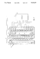
- FIG. 1 is a schematic, cross-sectional diagram of a liquid crystal display according to a preferred embodiment of the invention
- FIG. 2 is an exploded, isometric drawing, somewhat simplified, of the liquid crystal display of FIG. 1.
- FIG. 3 is a timing diagram useful in understanding the relationship between the time red, blue and green data are being written into the display of FIG. 1 and the spatial relationship between rows of red, blue, and green cathodoluminescent stripes;
- FIG. 4 is a schematic, cross-sectional diagram of a liquid crystal display according to an alternate embodiment of the invention.
- a liquid crystal display (LCD) 10 is shown to include a multi-color liquid crystal display panel 12, a light source 14, disposed behind the LCD panel 12 to backlight such panel 12, and a controller 16, for providing control signals to the display panel 12 and the light source 14, in a manner to be described hereinafter.
- the LCD display panel 12 includes a plurality of liquid crystal switching devices 18, one per pixel, arranged in a matrix of rows and columns, here three-hundred regularly spaced rows R 1 -R 300 .
- a polarizer 11 is disposed on one surface of the panel 12 and an analyzer 13 is disposed on the opposite surface of the panel 12, as shown in FIG. 1 (not shown in FIG. 2 for simplicity).
- the light source 14 is an electron tube 20 having disposed in an evacuated envelope 22 (not shown in FIG. 2) thereof, a plurality of, here 12, juxtapositioned cathodoluminescent stripes S 1 -S 12 regularly spaced from top to bottom and disposed on a suitable planar faceplate, or substrate, here a glass substrate 23 of the envelope 22 using any conventional deposition technique.
- the stripes S 1 -S 12 are disposed parallel to the rows R 1 -R 300 of switching devices 18. Hence, it follows that, in front of each one of the stripes S 1 -S 12 are twenty-five rows of the switching devices 18.
- the plurality of stripes S 1 -S 12 is arranged in groups, here into four groups 24 1 -24 4 , each group having included therein cathodoluminescent stripes adapted to produce all three of the primary colors.
- each one of the four groups 24 1 -24 4 is a triplet which includes three stripes adapted to produce red, green, and blue light, respectively, in response to striking electrons.
- stripes S 1 , S 4 , S 7 , S 10 produce red light
- stripes S 2 , S 5 , S 8 , S 11 produce blue light
- stripes S 3 , S 6 , S 9 , S 12 produce green light.
- a thin film 30 of electrically conductive material, here aluminum (not shown in FIG.
- cathodoluminescent stripes S 1 -S 12 is evaporated over the cathodoluminescent stripes S 1 -S 12 to provide an anode for the electron tube 20.
- thermionic cathodes K 1 -K 12 are disposed in the evacuated envelope of the tube.
- the cathodes K 1 -K 12 may alternatively be field emission cathodes or photo cathodes.
- the cathodes K 1 -K 12 are regularly spaced from top to bottom and are displaced laterally from the substrate 23, as shown. Each one of the cathodes K 1 -K 12 is adjacent to a corresponding one of a plurality of control grids CG 1 -CG 12 .
- the cathodes K 1 -K 12 are elongated structures disposed in a plane parallel to the plane of the substrate 23. Each one of the cathodes K 1 -K 12 is in registration with a corresponding set of the stripes S 1 -S 12 , here a corresponding one of the cathodoluminescent stripes S 1 -S 12 , respectively.
- a light diffuser 28 (not shown in FIG.
- the diffuser 28 may be integrally formed with the faceplate in the form of a ground glass surface, or could be a separate element such as an embossed plastic film which could, if desired, be bonded to the faceplate, as shown in FIG. 1.
- diffuser 28 improves illumination uniformity by selectively refracting light from the center of each one of the cathodoluminescent stripes towards the adjacent areas.
- the controller 16 provides addressing signals, to the LCD panel via a bus 40, such addressing signals being used to address the rows of switching devices while data are fed in parallel to all of the columns of switching devices 18 in the addressed row.
- addressing signals being used to address the rows of switching devices while data are fed in parallel to all of the columns of switching devices 18 in the addressed row.
- the control grids CG 1 -CG 12 for the cathodes K 1 -K 12 are turned on and off sequentially in accordance with the following Table where time is measured from the start of each frame.
- FIG. 3 a timing chart is shown where time is measured along the horizontal axis and space is measured along the vertical axis.
- the top of the vertical axis corresponds to the top of the display panel 12, and the bottom of the vertical axis corresponds to the bottom of the display panel 12.
- the chart is arranged in twelve vertical rows corresponding to the cathodoluminescent stripes S 1 -S 12 , respectively, and hence, likewise, corresponding to the cathodes K 1 -K 12 respectively, in registration with such stripes S 1 -S 12 .
- the time during which the control grid CG 1 -CG 12 , associated with the cathode K 1 -K 12 , respectively, allows electrons emitted by the cathodes K 1 -K 12 to pass to, and thereby strike, the cathodoluminescent stripe in registration therewith, (and thereby enable light of a particular color to be radiated by such cathodoluminescent stripe) is indicated by the shaded area. More particularly, the shaded areas indicated with vertical shading correspond to the time electrons strike the red stripes; the time during which electrons strike the green stripes is indicated by the shaded areas shown with diagonal shading; and, the shading with horizontal lines indicates the time when the blue stripes are being struck with electrons.
- the extension of the shading beyond the boundaries of the corresponding phosphor stripes indicates that the light from each stripe illuminates a three stripe-wide area (i.e., a triplet) on the panel 12.
- the second red stripe S 4 was not excited until the change of state of the devices 18 in row R 151 to allow time for all the switching devices 18 in rows R 51 -R 125 to assume their proper orientation for red before that part of the display was displayed in red, that is, the rows in registration with the second red stripe S 4 .
- the bottom green phosphor stripe S 12 is turned off well before state changes occur in devices 18 in row R 251 to allow time for the luminescence to decay by the time the LCD switching devices 18 are fully reset for displaying red information.
- the red color is swept from a first edge of the display (here the top) to the opposite edge of the display (here the bottom) and then the blue color is swept from the top to the bottom, the blue color sweep being initiated prior to the termination of the red color sweep.
- the green color is swept from the top to the bottom, such green sweep being initiated prior to the termination of the blue color sweep.
- the three colors appear to pass as three consecutive waves down the display. It is also noted that some time is allowed between termination of one color and the excitation of the next color, to allow for the finite time taken by the switching devices to change transmissivity in response to addressing signals.
- Minor modification may be needed in the on and off timing of the phosphor stripe excitation to account for such things as differences in phosphor decay times and spreading of light beyond the intended boundaries.
- Another likely modification will be the addition of a fractional-width green stripe with associated cathode and control grid at the top, and a fractional-width red stripe with associated cathode and control grid at the bottom, to allow the top and bottom edges of the display to be illuminated in all three colors.
- an alternative liquid crystal display 10' is shown to include the multi-color liquid crystal display panel 12 described above in connection with FIGS. 1 and 2.
- the light source 14' again includes an envelope 22' and a plurality of, here 12, juxtapositioned cathodoluminescent stripes S 1 -S 12 .
- the plurality of stripes S l -S 12 is arranged into sets, here four sets 241'-244', each set having included therein three of the cathodoluminescent stripes of the three primary colors.
- included within the envelope 22' are only four cathodes K 1 '-K 4 ', each one in registration with a corresponding one of the four sets of stripes 24 1 '-24 4 ', respectively, as shown.
- control grids CG 1 '-CG 4 ' Disposed around the rear, and side portions, of the cathodes K 1 '-K 4 ', are control grids CG 1 '-CG 4 ', respectively, as shown.
- a pair of deflection plates DP 1 -DP 4 , respectively, as shown.
- Each one of the pair of deflection plates DP 1 -DP 4 is similar to the pair of deflection plates used in a cathode ray tube.
- the controller 16' sequentially enables the control grids CG 1 '-CG 4 ' and also produces voltages for each one of the pair of deflection plates DP 1 -DP 4 .
- controller 16' when controller 16' enables control grid CG 1 ' to pass electrons emitted by cathode K 1 ' the controller 16'produces a three-step voltage sequence for the pair of deflection plates DP 1 to first direct electrons in an upwardly direction to strike stripe S 1 , to next direct electrons in a horizontal direction to strike stripe S 2 , and finally, to direct electrons in a downwardly direction to strike stripe S 3 .
- Control grids CG 2 ', CG 3 ' and CG 4 ' are sequentially enabled by controller 16' and, as each one of these control grids is enabled controller 16' produces the three step voltage sequence on the deflection plates DP 2 -DP 4 to thereby enable electrons emitted from cathodes K 1 '-K 4 ' to produce the illumination effect described above in connection with FIG. 3.
Landscapes
- Engineering & Computer Science (AREA)
- Physics & Mathematics (AREA)
- Computer Hardware Design (AREA)
- General Physics & Mathematics (AREA)
- Theoretical Computer Science (AREA)
- Liquid Crystal Display Device Control (AREA)
- Control Of Indicators Other Than Cathode Ray Tubes (AREA)
Abstract
Description
              TABLE
______________________________________
               Time "on" Time "off"
Control Grid   (ms)      (ms)
______________________________________
CG.sub.1       1.39      4.63
CG.sub.2       7.41      10.65
CG.sub.3       13.43     16.67
CG.sub.4       2.78      6.02
CG.sub.5       8.80      12.04
CG.sub.6       14.81     18.06
CG.sub.7       4.17      7.41
CG.sub.8       10.19     13.43
CG.sub.9       16.20     19.44
 CG.sub.10     5.56      8.80
 CG.sub.11     11.57     14.81
 CG.sub.12     17.59     20.83
CG.sub.1       18.06     21.30
______________________________________
Claims (25)
Priority Applications (1)
| Application Number | Priority Date | Filing Date | Title |
|---|---|---|---|
| US07/510,655 US5121233A (en) | 1990-04-18 | 1990-04-18 | Multi-color display |
Applications Claiming Priority (1)
| Application Number | Priority Date | Filing Date | Title |
|---|---|---|---|
| US07/510,655 US5121233A (en) | 1990-04-18 | 1990-04-18 | Multi-color display |
Publications (1)
| Publication Number | Publication Date |
|---|---|
| US5121233A true US5121233A (en) | 1992-06-09 |
Family
ID=24031623
Family Applications (1)
| Application Number | Title | Priority Date | Filing Date |
|---|---|---|---|
| US07/510,655 Expired - Fee Related US5121233A (en) | 1990-04-18 | 1990-04-18 | Multi-color display |
Country Status (1)
| Country | Link |
|---|---|
| US (1) | US5121233A (en) |
Cited By (29)
| Publication number | Priority date | Publication date | Assignee | Title |
|---|---|---|---|---|
| US5387921A (en) * | 1992-10-08 | 1995-02-07 | Panocorp Display Systems | Scanning back illuminating light source for liquid crystal and other displays |
| US5396406A (en) * | 1993-02-01 | 1995-03-07 | Display Technology Industries | Thin high efficiency illumination system for display devices |
| US5398086A (en) * | 1991-03-20 | 1995-03-14 | Mitsubishi Denki Kabushiki Kaisha | Projection type display device |
| US5402143A (en) * | 1991-12-23 | 1995-03-28 | Panocorp Display Systems | Color fluorescent liquid crystal display |
| US5428366A (en) * | 1992-09-09 | 1995-06-27 | Dimension Technologies, Inc. | Field sequential color illumination system for liquid crystal display |
| US5461397A (en) * | 1992-10-08 | 1995-10-24 | Panocorp Display Systems | Display device with a light shutter front end unit and gas discharge back end unit |
| US5467085A (en) * | 1992-11-10 | 1995-11-14 | Avionic Displays Corporation | Display for electronic indicator |
| US5760858A (en) * | 1995-04-21 | 1998-06-02 | Texas Instruments Incorporated | Field emission device panel backlight for liquid crystal displays |
| US5896098A (en) * | 1992-12-30 | 1999-04-20 | Advanced Displays Corporation | Self-contained multifunctional LCD flight indicator |
| US5940163A (en) * | 1994-07-19 | 1999-08-17 | Electro Plasma Inc. | Photon coupled color flat panel display and method of manufacture |
| WO1999050817A1 (en) * | 1998-03-27 | 1999-10-07 | Central Research Laboratories Limited | Blacklight control for a display device |
| US6184850B1 (en) * | 1991-09-04 | 2001-02-06 | Canon Kabushiki Kaisha | Image display apparatus with backlit display and method of driving the same |
| US20010001337A1 (en) * | 1999-03-15 | 2001-05-24 | Charles M. Storrs Et Al | Debris access door |
| US6243067B1 (en) * | 1996-05-24 | 2001-06-05 | Matsushita Electric Industrial Co., Ltd. | Liquid crystal projector |
| US20020080105A1 (en) * | 2000-12-27 | 2002-06-27 | Tsuneo Sato | Transmissive color liquid crystal display |
| US6448951B1 (en) * | 1998-05-11 | 2002-09-10 | International Business Machines Corporation | Liquid crystal display device |
| US6509887B1 (en) * | 1997-06-20 | 2003-01-21 | Citizen Watch Co., Ltd. | Anti-ferroelectric liquid crystal display and method of driving the same |
| US6559827B1 (en) * | 2000-08-16 | 2003-05-06 | Gateway, Inc. | Display assembly |
| US20030193455A1 (en) * | 1999-04-22 | 2003-10-16 | Tadashi Mizohata | Multiplex anode matrix vacuum fluorescent display and the driving device therefor |
| US6683659B2 (en) * | 2000-09-14 | 2004-01-27 | Koninklijke Philips Electronics N.V. | Liquid crystal display screen with backlighting |
| US20040017348A1 (en) * | 1999-10-08 | 2004-01-29 | Sharp Kabushiki Kaisha | Display device and light source |
| WO2004044878A3 (en) * | 2002-11-05 | 2004-07-01 | 3M Innovative Properties Co | Swept illumination to overcome lcd lag in front and rear projection displays |
| US20060055659A1 (en) * | 2004-09-10 | 2006-03-16 | Industrial Technology Research Institute | Method for modulating and driving backlight sources for flat panel displays |
| US20060103639A1 (en) * | 2004-11-16 | 2006-05-18 | Nec Lcd Technologies, Ltd | Display device |
| US20070070023A1 (en) * | 2005-09-27 | 2007-03-29 | Kozo Yasuda | Liquid crystal display device |
| US20070200792A1 (en) * | 2006-02-27 | 2007-08-30 | Samsung Electronics Co., Ltd. | High resolution 2D-3D switchable autostereoscopic display apparatus |
| CN100525576C (en) * | 2004-09-17 | 2009-08-05 | 财团法人工业技术研究院 | Back light source modulation method for plane display |
| CN100584142C (en) * | 2004-09-17 | 2010-01-20 | 财团法人工业技术研究院 | Method for modulating backlight source of flat panel display |
| US20120002132A1 (en) * | 2010-07-02 | 2012-01-05 | Semiconductor Energy Laboratory Co., Ltd. | Driving method of liquid crystal display device |
Citations (15)
| Publication number | Priority date | Publication date | Assignee | Title |
|---|---|---|---|---|
| US3924227A (en) * | 1972-11-13 | 1975-12-02 | Michael Stolov | Digital display device |
| US4368485A (en) * | 1981-04-13 | 1983-01-11 | Zenith Radio Corporation | Billboard large screen TV |
| JPS60149028A (en) * | 1984-01-13 | 1985-08-06 | Ricoh Co Ltd | LCD color display device |
| US4611889A (en) * | 1984-04-04 | 1986-09-16 | Tektronix, Inc. | Field sequential liquid crystal display with enhanced brightness |
| JPS6252533A (en) * | 1985-09-02 | 1987-03-07 | Nippon Telegr & Teleph Corp <Ntt> | Liquid crystal color display panel |
| US4720655A (en) * | 1984-09-17 | 1988-01-19 | Sanyo Electric Co., Ltd. | Flat color cathode-ray tube with phosphor index stripes |
| EP0267686A1 (en) * | 1986-10-23 | 1988-05-18 | Litton Systems Canada Limited | Full colour liquid crystal display |
| JPS643631A (en) * | 1987-06-26 | 1989-01-09 | Toshiba Corp | Liquid crystal display device |
| US4822144A (en) * | 1986-12-24 | 1989-04-18 | U.S. Philips Corporation | Electro-optic color display including luminescent layer and interference filter |
| US4830469A (en) * | 1987-02-13 | 1989-05-16 | U.S. Philips Corporation | Liquid crystalline color display cell having a phosphorescent substrate and U.V.-absorbing dichroic dye |
| US4838660A (en) * | 1983-03-30 | 1989-06-13 | Manchester R & D Partnership | Colored encapsulated liquid crystal apparatus using enhanced scattering |
| US4857900A (en) * | 1984-12-15 | 1989-08-15 | Canon Kabushiki Kaisha | Display device with color correction |
| US4865425A (en) * | 1985-12-03 | 1989-09-12 | Stanley Electric Co., Ltd. | Power source device for driving liquid crystal |
| US4870484A (en) * | 1983-05-13 | 1989-09-26 | Seiko Epson Corporation | Color display device using light shutter and color filters |
| US4915479A (en) * | 1986-12-17 | 1990-04-10 | U.S. Philips Corporation | Liquid crystal display illumination system |
-
1990
- 1990-04-18 US US07/510,655 patent/US5121233A/en not_active Expired - Fee Related
Patent Citations (16)
| Publication number | Priority date | Publication date | Assignee | Title |
|---|---|---|---|---|
| US3924227A (en) * | 1972-11-13 | 1975-12-02 | Michael Stolov | Digital display device |
| US4368485A (en) * | 1981-04-13 | 1983-01-11 | Zenith Radio Corporation | Billboard large screen TV |
| US4838660A (en) * | 1983-03-30 | 1989-06-13 | Manchester R & D Partnership | Colored encapsulated liquid crystal apparatus using enhanced scattering |
| US4870484A (en) * | 1983-05-13 | 1989-09-26 | Seiko Epson Corporation | Color display device using light shutter and color filters |
| JPS60149028A (en) * | 1984-01-13 | 1985-08-06 | Ricoh Co Ltd | LCD color display device |
| US4611889A (en) * | 1984-04-04 | 1986-09-16 | Tektronix, Inc. | Field sequential liquid crystal display with enhanced brightness |
| US4720655A (en) * | 1984-09-17 | 1988-01-19 | Sanyo Electric Co., Ltd. | Flat color cathode-ray tube with phosphor index stripes |
| US4857900A (en) * | 1984-12-15 | 1989-08-15 | Canon Kabushiki Kaisha | Display device with color correction |
| JPS6252533A (en) * | 1985-09-02 | 1987-03-07 | Nippon Telegr & Teleph Corp <Ntt> | Liquid crystal color display panel |
| US4865425A (en) * | 1985-12-03 | 1989-09-12 | Stanley Electric Co., Ltd. | Power source device for driving liquid crystal |
| US4799050A (en) * | 1986-10-23 | 1989-01-17 | Litton Systems Canada Limited | Full color liquid crystal display |
| EP0267686A1 (en) * | 1986-10-23 | 1988-05-18 | Litton Systems Canada Limited | Full colour liquid crystal display |
| US4915479A (en) * | 1986-12-17 | 1990-04-10 | U.S. Philips Corporation | Liquid crystal display illumination system |
| US4822144A (en) * | 1986-12-24 | 1989-04-18 | U.S. Philips Corporation | Electro-optic color display including luminescent layer and interference filter |
| US4830469A (en) * | 1987-02-13 | 1989-05-16 | U.S. Philips Corporation | Liquid crystalline color display cell having a phosphorescent substrate and U.V.-absorbing dichroic dye |
| JPS643631A (en) * | 1987-06-26 | 1989-01-09 | Toshiba Corp | Liquid crystal display device |
Non-Patent Citations (10)
| Title |
|---|
| "10.1: Progress of the Flat Channel Multiplier CRT", D. Washington et al., 1985 pp. 166-169. |
| "Cathodoluminescent Back Light for Liquid Crystal Device", Research Disclosure, Jan. 1991, No. 321. |
| "Flat-Panel Displays and CRTs", L. E. Tannas, Jr., 1985 p. 14. |
| "Spindt Cold Cathode Vacuum Fluorescent Display", SRI International, C. E. Holland et al., Sep. 1987 pp. 1-3. |
| 10.1: Progress of the Flat Channel Multiplier CRT , D. Washington et al., 1985 pp. 166 169. * |
| Cathodoluminescent Back Light for Liquid Crystal Device , Research Disclosure, Jan. 1991, No. 321. * |
| Flat Panel Displays and CRTs , L. E. Tannas, Jr., 1985 p. 14. * |
| Seminar 1.2, "Vacuum Fluorescent Displays", K. Morimoto et al., May 1986. |
| Seminar 1.2, Vacuum Fluorescent Displays , K. Morimoto et al., May 1986. * |
| Spindt Cold Cathode Vacuum Fluorescent Display , SRI International, C. E. Holland et al., Sep. 1987 pp. 1 3. * |
Cited By (40)
| Publication number | Priority date | Publication date | Assignee | Title |
|---|---|---|---|---|
| US5398086A (en) * | 1991-03-20 | 1995-03-14 | Mitsubishi Denki Kabushiki Kaisha | Projection type display device |
| US6184850B1 (en) * | 1991-09-04 | 2001-02-06 | Canon Kabushiki Kaisha | Image display apparatus with backlit display and method of driving the same |
| US5402143A (en) * | 1991-12-23 | 1995-03-28 | Panocorp Display Systems | Color fluorescent liquid crystal display |
| US5428366A (en) * | 1992-09-09 | 1995-06-27 | Dimension Technologies, Inc. | Field sequential color illumination system for liquid crystal display |
| US5387921A (en) * | 1992-10-08 | 1995-02-07 | Panocorp Display Systems | Scanning back illuminating light source for liquid crystal and other displays |
| US5461397A (en) * | 1992-10-08 | 1995-10-24 | Panocorp Display Systems | Display device with a light shutter front end unit and gas discharge back end unit |
| US5467085A (en) * | 1992-11-10 | 1995-11-14 | Avionic Displays Corporation | Display for electronic indicator |
| US5896098A (en) * | 1992-12-30 | 1999-04-20 | Advanced Displays Corporation | Self-contained multifunctional LCD flight indicator |
| US5396406A (en) * | 1993-02-01 | 1995-03-07 | Display Technology Industries | Thin high efficiency illumination system for display devices |
| US5940163A (en) * | 1994-07-19 | 1999-08-17 | Electro Plasma Inc. | Photon coupled color flat panel display and method of manufacture |
| US5760858A (en) * | 1995-04-21 | 1998-06-02 | Texas Instruments Incorporated | Field emission device panel backlight for liquid crystal displays |
| US6243067B1 (en) * | 1996-05-24 | 2001-06-05 | Matsushita Electric Industrial Co., Ltd. | Liquid crystal projector |
| US7102603B2 (en) | 1997-06-20 | 2006-09-05 | Citizen Watch Co., Ltd. | Liquid crystal display and method of driving the same |
| US6509887B1 (en) * | 1997-06-20 | 2003-01-21 | Citizen Watch Co., Ltd. | Anti-ferroelectric liquid crystal display and method of driving the same |
| WO1999050817A1 (en) * | 1998-03-27 | 1999-10-07 | Central Research Laboratories Limited | Blacklight control for a display device |
| US6448951B1 (en) * | 1998-05-11 | 2002-09-10 | International Business Machines Corporation | Liquid crystal display device |
| US20010001337A1 (en) * | 1999-03-15 | 2001-05-24 | Charles M. Storrs Et Al | Debris access door |
| US20030193455A1 (en) * | 1999-04-22 | 2003-10-16 | Tadashi Mizohata | Multiplex anode matrix vacuum fluorescent display and the driving device therefor |
| US20040017348A1 (en) * | 1999-10-08 | 2004-01-29 | Sharp Kabushiki Kaisha | Display device and light source |
| US7742031B2 (en) * | 1999-10-08 | 2010-06-22 | Sharp Kabushiki Kaisha | Display device and light source |
| US20090237349A1 (en) * | 1999-10-08 | 2009-09-24 | Takaji Numao | Display device and light source |
| US8179364B2 (en) | 1999-10-08 | 2012-05-15 | Sharp Kabushiki Kaisha | Display device and light source |
| US6559827B1 (en) * | 2000-08-16 | 2003-05-06 | Gateway, Inc. | Display assembly |
| US6683659B2 (en) * | 2000-09-14 | 2004-01-27 | Koninklijke Philips Electronics N.V. | Liquid crystal display screen with backlighting |
| US6690348B2 (en) * | 2000-12-27 | 2004-02-10 | Mitsubishi Denki Kabushiki Kaisha | Transmissive color liquid crystal display |
| US20020080105A1 (en) * | 2000-12-27 | 2002-06-27 | Tsuneo Sato | Transmissive color liquid crystal display |
| WO2004044878A3 (en) * | 2002-11-05 | 2004-07-01 | 3M Innovative Properties Co | Swept illumination to overcome lcd lag in front and rear projection displays |
| US20040135754A1 (en) * | 2002-11-05 | 2004-07-15 | Conner Arlie R. | Swept illumination to reduce LCD lag in front and rear projection displays |
| US7196687B2 (en) | 2002-11-05 | 2007-03-27 | 3M Innovative Properties Company | Swept illumination to reduce LCD lag in front and rear projection displays |
| CN100416644C (en) * | 2002-11-05 | 2008-09-03 | 3M创新有限公司 | Method and display for illuminating a liquid crystal panel |
| US20060055659A1 (en) * | 2004-09-10 | 2006-03-16 | Industrial Technology Research Institute | Method for modulating and driving backlight sources for flat panel displays |
| US7583248B2 (en) * | 2004-09-10 | 2009-09-01 | Industrial Technology Research Institute | Method for modulating and driving backlight sources for flat panel displays |
| CN100584142C (en) * | 2004-09-17 | 2010-01-20 | 财团法人工业技术研究院 | Method for modulating backlight source of flat panel display |
| CN100525576C (en) * | 2004-09-17 | 2009-08-05 | 财团法人工业技术研究院 | Back light source modulation method for plane display |
| US20060103639A1 (en) * | 2004-11-16 | 2006-05-18 | Nec Lcd Technologies, Ltd | Display device |
| US20070070023A1 (en) * | 2005-09-27 | 2007-03-29 | Kozo Yasuda | Liquid crystal display device |
| US20070200792A1 (en) * | 2006-02-27 | 2007-08-30 | Samsung Electronics Co., Ltd. | High resolution 2D-3D switchable autostereoscopic display apparatus |
| US8373684B2 (en) * | 2006-02-27 | 2013-02-12 | Samsung Electronics Co., Ltd. | High resolution 2D-3D switchable autostereoscopic display apparatus |
| US20120002132A1 (en) * | 2010-07-02 | 2012-01-05 | Semiconductor Energy Laboratory Co., Ltd. | Driving method of liquid crystal display device |
| US8988337B2 (en) * | 2010-07-02 | 2015-03-24 | Semiconductor Energy Laboratory Co., Ltd. | Driving method of liquid crystal display device |
Similar Documents
| Publication | Publication Date | Title |
|---|---|---|
| US5121233A (en) | Multi-color display | |
| US5347201A (en) | Display device | |
| US4907862A (en) | Method for generating elecronically controllable color elements and color display based on the method | |
| US5760858A (en) | Field emission device panel backlight for liquid crystal displays | |
| US4978952A (en) | Flat screen color video display | |
| US5592193A (en) | Backlighting arrangement for LCD display panel | |
| JP2002503832A (en) | Tiled electronic display structure | |
| JPH0728414A (en) | Electronic luminescence display system | |
| WO2000068732A1 (en) | Display with active contrast enhancement | |
| US6429836B1 (en) | Circuit and method for display of interlaced and non-interlaced video information on a flat panel display apparatus | |
| US20100060820A1 (en) | Screen structure for field emission device backlighting unit | |
| JPH0261949A (en) | Fluorescent microdot screen and its addressing method | |
| JP2926612B2 (en) | Field emission device, field emission image display device, and method of driving the same | |
| KR101299035B1 (en) | Liquid crystal display having a field emission backlight | |
| US5359260A (en) | Displays | |
| US5381252A (en) | Opposed scanning electron beams light source for projection LCD | |
| US5521660A (en) | Multimedia field emission device portable projector | |
| JP2836445B2 (en) | Image display device and image display drive circuit | |
| US5303054A (en) | Line electron beam light source for projection LCD system | |
| JPH0969332A (en) | Field emission type of display element | |
| JP2555019B2 (en) | Driving method for fluorescent display tube | |
| CN1083934A (en) | Color fluorescent liquid crystal display | |
| JPS6089042A (en) | Color display device | |
| JPH01117251A (en) | Image display device | |
| JPH0588169A (en) | Color display device and flat light source |
Legal Events
| Date | Code | Title | Description |
|---|---|---|---|
| AS | Assignment |
Owner name: RAYTHEON COMPANY, A CORP. OF DELAWARE, MASSACHUSET Free format text: ASSIGNMENT OF ASSIGNORS INTEREST.;ASSIGNOR:SPENCER, GORDON R.;REEL/FRAME:005279/0886 Effective date: 19900411 Owner name: HARRIS CORPORATION, A CORP. OF DELAWARE, FLORIDA Free format text: ASSIGNMENT OF ASSIGNORS INTEREST.;ASSIGNOR:KANALY, DAVID B.;REEL/FRAME:005279/0888 Effective date: 19900413 |
|
| FEPP | Fee payment procedure |
Free format text: PAYER NUMBER DE-ASSIGNED (ORIGINAL EVENT CODE: RMPN); ENTITY STATUS OF PATENT OWNER: LARGE ENTITY Free format text: PAYOR NUMBER ASSIGNED (ORIGINAL EVENT CODE: ASPN); ENTITY STATUS OF PATENT OWNER: LARGE ENTITY |
|
| FEPP | Fee payment procedure |
Free format text: PAYER NUMBER DE-ASSIGNED (ORIGINAL EVENT CODE: RMPN); ENTITY STATUS OF PATENT OWNER: LARGE ENTITY |
|
| REFU | Refund |
Free format text: REFUND PROCESSED. MAINTENANCE FEE HAS ALREADY BEEN PAID (ORIGINAL EVENT CODE: R160); ENTITY STATUS OF PATENT OWNER: LARGE ENTITY |
|
| FPAY | Fee payment |
Year of fee payment: 4 |
|
| FEPP | Fee payment procedure |
Free format text: PAYOR NUMBER ASSIGNED (ORIGINAL EVENT CODE: ASPN); ENTITY STATUS OF PATENT OWNER: LARGE ENTITY |
|
| REMI | Maintenance fee reminder mailed | ||
| LAPS | Lapse for failure to pay maintenance fees | ||
| FP | Lapsed due to failure to pay maintenance fee |
Effective date: 20000609 |
|
| STCH | Information on status: patent discontinuation |
Free format text: PATENT EXPIRED DUE TO NONPAYMENT OF MAINTENANCE FEES UNDER 37 CFR 1.362 |