BACKGROUND OF THE INVENTION
The present invention generally relates to a phase inverter, and more particularly to a phase inverter which receives a radio frequency signal and derives two radio frequency signals having a phase difference of 180° therefrom. Further, the present invention is directed to a push-pull amplifier using such a phase inverter.
Conventionally, it is known to form a phase inverter by the use of a transformer, a capacitor or an inductor. Such a phase inverter is suitable for a low-frequency range. In other words, the use of a transformer, a capacitor or an inductor is not suitable for a very high frequency range in the order of tens of giga-hertz or higher because of the presence of stray capacitance. From this reason, it is necessary to use a distributed element circuit such as a coupled line network in the range of very high frequencies (microwave range).
Referring to FIG. 1, there is illustrated a conventional phase inverter using parallel coupled lines. Ring-shaped transmission lines 2 and 3 formed of a conductive material are arranged on a dielectric substrate 1 so that two networks each composed of two λ/4 parallel coupled lines are formed (λ is the wavelength of a signal applied to the transmission line 3). The transmission line 2 has terminals 42, 43 and 44, and the transmission line 3 has a terminal 41. Two adjacent terminals among the terminals 41, 42, 43 and 44 have a phase difference of 90°. A signal applied to the terminal 41 is equally distributed to the terminals 42 and 44. A signal output from the terminal 42 has the +90° phase difference with respect to the input signal, and a signal output from the terminal 44 has the -90° phase difference with respect to the input signal. Thus, the signals having a phase difference of 180° are output through the terminals 42 and 44. In this case, the signals output from the terminals 42 and 44 are combined together at the terminal 43. However, since the signals at the terminals 42 and 44 are 180° out of phase, no signal is output from the terminal 43.
FIG. 2A is a graph of amplitude vs. normalized frequency characteristics of the conventional phase inverter shown in FIG. 1, and FIG. 2B is a graph of phase vs. normalized frequency characteristics thereof. A curve I is a characteristic of a signal passing from the terminal 41 to the terminal 42. A curve II is a characteristic of a signal passing from the terminal 41 to the terminal 44. It can be seen from FIG. 2A that the amplitude characteristic of the signal passing from the terminal 41 to the terminal 42 is approximately flat in the ±0.4f0 range where f0 is the center frequency of this signal (equal to 12.5 GHz, for example). On the other hand, the amplitude characteristic of the signal passing from the terminal 41 to the terminal 44 is approximately flat only in the ±0.2f0 range. Such a range is narrow and insufficient in view of practical board-band use.
It can be seen from FIG. 2B that the phase characteristics of the signal passing from the terminal 41 to the terminal 42 and the signal passing from the terminal 41 to the terminal 44 have a phase difference of 180° in a range of ±0.4f0. From the above-mentioned reasons, it is desired to provide a phase inverter in which the amplitude and phase characteristics of two 180° out-of-phase output signals are both flat in a wider frequency range.
SUMMARY OF THE INVENTION
It is a general object of the present invention to provide an improved phase inverter in which the aforementioned disadvantages are eliminated.
A more specific object of the present invention is to provide a phase inverter in which the amplitude and phase characteristics of two output signals having a phase difference of 180° are both flat in a wider very-high frequency range.
The above objects of the present invention are achieved by a phase inverter comprising first, second, third and fourth terminals, a first coupling circuit coupled between the first and second terminals, a second coupling circuit coupled between the second and third terminals, a third coupling circuit coupled between the third and fourth terminals, and a fourth coupling circuit coupled between the first and fourth terminals. The first to fourth terminals and the first to fourth coupling circuits are arranged into a ring. The first coupling circuit is of a type different from a type of the fourth coupling circuit. The second and third coupling circuits are identical in type. Two output signals having a phase difference of 180° are drawn from the second and fourth terminal when an input terminal is applied to the first terminal, and an output signal is drawn from the first terminal when two input signals having a phase difference of 180° are applied to the second and fourth terminals.
Another object of the present invention is to provide a push-pull amplifier using the above-mentioned phase inverter.
This object of the present invention is achieved by a push-pull amplifier comprising a first phase inverter having an input terminal receiving an input signal and two output terminals, a second phase inverter having two input terminals and an output terminal outputting an output signal, a first amplifier coupled between one of the two output terminals of the first phase inverter and one of the two input terminals of the second phase inverter, and a second amplifier coupled between the other output terminal of the first phase inverter and the other input terminal of the second phase inverter. Each of the first and second phase inverters includes first, second, third and fourth terminals, a first coupling circuit coupled between the first and second terminals, a second coupling circuit coupled between the second and third terminals, a third coupling circuit coupled between the third and fourth terminals, and a fourth coupling circuit coupled between the first and fourth terminals. The first to fourth terminals and the first to fourth coupling circuits are arranged into a ring. The first coupling circuit is of a type different from a type of the fourth coupling circuit, and the second and third coupling circuits being identical in type. The first, second, and fourth terminals of the first phase inverter are the input terminal and the two output terminals thereof, respectively. The first, second and fourth terminals of the second phase inverter are the two input terminals and the output terminal thereof, respectively. The third terminals of the first and second phase inverters are grounded through first and second resistors, respectively.
Additional objects, features and advantages of the present invention will become apparent from the following detailed description when read in conjunction with the accompanying drawings.
BRIEF DESCRIPTION OF THE DRAWINGS
FIG. 1 is a diagram of a conventional phase inverter;
FIG. 2A is a graph illustrating amplitude vs. normalized frequency characteristics of the phase inverter shown in FIG.1;
FIG. 2B is a graph illustrating phase vs. normalized frequency characteristics of the phase inverter shown in FIG. 1;
FIG. 3 is a diagram illustrating the principle of the present invention;
FIG. 4A is a diagram of a phase inverter according to a first embodiment of the present invention;
FIG. 4B is a diagram of another phase inverter according to the first embodiment of the present invention;
FIGS. 5A and 5B are diagrams illustrating λ/4 parallel coupled line networks;
FIG. 6A is a diagram of a phase inverter according to a second embodiment of the present invention;
FIG. 6B is a diagram of another phase inverter according to the second embodiment of the present invention;
FIG. 7 is a diagram of a directional coupler;
FIG. 8A is a graph of amplitude vs. normalized frequency characteristics of the embodiment shown in FIG.6A;
FIG. 8B is a graph of phase vs. normalized frequency characteristics of the embodiment shown in FIG.6A;
FIG. 9A through 9D are diagrams of variations of the arrangements shown in FIGS.4A and 4B;
FIG. 10A is a diagram of a variation of the arrangements shown in FIGS.4A and 4B;
FIGS. 10B and 10C are diagrams of modifications of the first and second embodiments, respectively;
FIG. 10D is a diagram of an arrangement equivalent to the arrangement shown in FIG.10B;
FIG. 11A is a diagram of a variation of the phase inverter according to the first embodiment of the present invention;
FIGS. 11B through 11D are diagrams illustrating structures of transmission lines;
FIG. 12 is a diagram illustrating the principle of a phase inverter according to a third embodiment of the present invention in which coupling circuits are formed by waveguide directional couplers;
FIG. 13A is a plan view of the third embodiment of the present invention;
FIG. 13B is a front view of the third embodiment of the present invention;
FIG. 14A is a perspective view of a waveguide directional coupler used in the third embodiment of the present invention;
FIG. 14B is a perspective view of another waveguide directional coupler used in the third embodiment of the present invention;
FIG. 15A and 15B are diagrams showing the types of the third embodiment;
FIG. 16 is a circuit diagram of a push-pull amplifier to which the phase inverter of the present invention is applied;
FIG. 17 is a diagram illustrating a first configuration of the push-pull amplifier according to the present invention;
FIG. 18 is a diagram illustrating a second configuration of the push-pull amplifier according to the present invention; and
FIG. 19 is a diagram illustrating a third configuration of the push-pull amplifier according to the present invention.
DESCRIPTION OF THE PREFERRED EMBODIMENTS
FIG. 3 is a diagram illustrating the principle of the present invention. A phase inverter according to the present invention includes coupling circuits 1001, 1002, 1003 and 1004 each formed by λ/4 parallel coupled lines. The coupling circuits 1001 -1004 are arranged into a ring and coupled to each other through terminals 101, 102, 103 and 104 as shown in FIG.3. When two output signals are derived from an input signal, the terminal 101 serves as an input terminal of the phase inverter, and the terminals 102 and 104 serve as output terminals thereof. When an input signal is applied to the input terminal 101, 180° out-of-phase signals are drawn from the output terminals 102 and 104. No signal is drawn from the terminal 103.
The type of the coupling circuit 1001 between the input terminal 101 and the output terminal 102 is different from that of the coupling circuit 1004 between the input terminal 101 and the output terminal 104. For example, the coupling circuit 1001 is formed by open coupled lines, and the coupling circuit 1004 is formed by grounded coupled lines. On the other hand, the type of the coupling circuit 1002 is the same as that of the coupling circuit 1003. That is, the coupling circuits 1002 and 1003 are formed by open coupled lines or grounded coupled lines.
Alternatively, the terminals 102 and 104 serve as input terminals, and the terminal 101 serves as an output terminal. In this alternative, two 180° out-of-phase input signals are applied to the terminals 102 and 104 and combined, and an output signal is drawn from the output terminal 101.
FIG. 4A is a plan view of a phase inverter according to a first embodiment of the present invention. The phase inverter includes transmission lines 101, 102, 103 and 104, each of which is in the shape of a substantially half circle. The transmission lines 101 -104 are arranged on a dielectric substrate 1 so as to form a ring. The transmission lines 101, 102, 103 and 104 have terminals 20, 21, 22 and 23, respectively. Opposite portions of adjacent transmission lines form λ/4 parallel coupled lines by which a coupling circuit (network of λ/4 parallel coupled lines) is formed. That is, four coupling circuits or networks are connected through the terminals 20-23 as shown in FIG. 4A. In FIG. 4A, "o" indicates an open end of a transmission line, and "○" indicates a grounded end of a transmission line.
A network composed of λ/4 parallel coupled lines is classified into either a double-end open type or a double-end grounded type. FIG. 5A shows a λ/4 parallel coupled line network of the double-end open type, and FIG. 5B shows a λ/4 parallel coupled line network of the double-end grounded type. The λ/4 parallel coupled line networks shown in FIGS. 5A and 5B function as bandpass filters. The phase difference between a terminal 11 of one of the two transmission lines shown in FIG. 5A and a terminal 12 of the other transmission line is equal to +90° at the center frequency f0. There is a -90° phase difference between a terminal 13 of one of the two transmission lines shown in FIG. 5B and a terminal 14 of the other transmission line at the center frequency f0.
Turning to FIG. 4A, λ/4 parallel coupled line networks of the double-end open type (coupling circuits) are respectively provided between the terminals 20 and 21, terminals 21 and 22, and terminals 22 and 23. A λ/4 parallel coupled line network of the double-end grounded type (a coupling circuit) is provided between the terminals 20 and 23. The type of the network between the input terminal 20 and the output terminal 21 is different from the type of the network between the input terminal 20 and the output terminal 23. The network between the terminals 21 and 22 is of the same type as the network between the terminals 22 and 23. When the input signal is applied to the input terminal 20, 180° out-of-phase signals having the same amplitude are drawn from the output terminals 21 and 23. Particularly at the center frequency f0, there is a +90° phase difference between the input terminal 20 and the output terminal 21, and a -90° phase difference between the input terminal 20 and the output terminal 23. In an alternative use of the phase inverter shown in FIG. 4A, the terminals 21 and 23 serve as input terminals, and the terminal 20 serves as an output terminal. Two 180° out-of-phase signals applied to the terminals 21 and 23 are combined together so that a combined output signal is obtained at the terminal 20.
The first embodiment of the present invention employs four λ/4 parallel coupled line networks provided between the individual adjacent terminals. This arrangement of the first embodiment is apparently distinguishable from the conventional arrangement shown in FIG. 1. The amplitude characteristics of the output signals are flat in an improved range of ±0.3f0.
In FIG. 4B, a λ/4 parallel coupled line network of the double-end open type is provided between the input terminal 20 and the output terminal 21, and λ/4 parallel coupled line networks of the double-end grounded type are provided between the terminals 21 and 22, terminals 22 and 23, and terminals 20 and 23. The type of the network between the input terminal 20 and the output terminal 21 is different from the type of the input terminal 20 and the output terminal 23. The arrangement shown in FIG. 4B presents an improved amplitude flat range of ±0.3f0.
FIG. 6A is a diagram of a phase inverter according to a second embodiment of the present invention. The second embodiment uses directional couplers which are networks each composed of parallel coupled lines. Networks (directional couplers) 351, 352, 353 and 354 are of the ring coupler type and are arranged into a ring on the dielectric substrate 1. Terminals 30, 31, 32 and 33 are provided between individual adjacent directional couplers among the directional couplers 351 -354. As shown in FIG.7, each of the directional couplers 351 -354 has a plurality of comb-shaped interdigital transmission lines. The transmission lines are electrically coupled to alternate transmission lines through conducting jump wires 39. The directional coupler has four terminals 35, 36, 37 and 38. In a directional coupler of the open type, the terminal 35 (couple port) and the terminal 36 (main port) are both open. In a directional coupler of the grounded type, the terminals 35 and 36 are both grounded. In the open type directional coupler, there is a 90° phase difference between the terminal 37 (input port) and the terminal 38 (isolation port) at the center frequency f0. In the grounded type directional coupler, there is a -90° phase difference between the terminals 37 and 38 at the center frequency f0. The directional coupler shown in FIG.7 itself is known to a person having ordinary skill in the art.
Turning to FIG. 6A, the directional couplers 351, 352 and 353 respectively provided between the terminals 30 and 31, 31 and 32, and 32 and 33 are of the open type, and the directional coupler 354 provided between the terminals 30 and 33 is of the grounded type. When an input signal is applied to the input terminal 30, 180° out-of-phase signals are drawn from the output terminals 31 and 33. Particularly at the center frequency f0, there is a +90° phase difference between the terminals 30 and 31, and a -90° phase difference between the terminals 30 and 33.
Three directional couplers shown in FIG. 6B provided between the terminals 31 and 32, 32 and 33, and 33 and 30 are of the grounded type, and the remaining directional coupler provided between the terminals 30 and 31 is of the open type. When an input signal is applied to the input terminal 30, 180° out-of-phase signals are drawn from the output terminals 31 and 33. Particularly at the center frequency f0, there is the +90° phase difference between the terminals 30 and 31, and the -90° phase difference between the terminals 30 and 33.
FIG. 8A is a graph illustrating amplitude vs. normalized frequency characteristics of signals passing through the phase inverter shown in FIG. 6A. FIG. 8B is a graph illustrating phase vs. normalized frequency characteristics of signals passing therethrough. A curve III shows frequency characteristics of a signal passing from the input terminal 30 to the output terminal 31, and a curve IV shows frequency characteristics of a signal passing from the input terminal 30 to the output terminal 33. The amplitude characteristics of the signals III and IV are both flat in the ±0.4f0 range (the center frequency f0 is 12.5 GHz, for example). The amplitude characteristics of signals are considerably improved as compared with those for the conventional phase inverter shown in FIG. 1. The 180° phase difference between the signals is obtained in the ±0.4f0 range. In an alternative use, the terminals 31 and 33 serve as input terminals, and the terminal 30 serves as an output terminal.
FIGS. 9A through 9D respectively show variations of the aforementioned first embodiments. A variety of patterns of transmission line is shown.
The transmission lines of the aforementioned individual phase inverters have the same pattern width.
For example, the transmission lines 101 -104 shown in FIG. 4A have the same pattern width. Similarly, as shown in FIG. 10A. networks 36-39 provided between terminals 40-43 are individually composed of two coupled lines having the same pattern width. The terminals 40-43 have the same impedance.
A modification of the phase inverter shown in FIG. 10A is illustrated in FIG.1OB. The phase inverter shown in FIG. 10B also functions as an impedance converter. The phase inverter includes networks (coupling circuits) 45, 46, 47 and 48 provided between the terminals 50, 51, 52 and 53. Each of the networks 45-48 is formed by a pair of transmission lines W1 and W2. The transmission line W1 is wider than the transmission line W2 (W1>W2). Each of the terminals 50 and 52 has high impedance (H), and each of the terminals 51 and 53 has low impedance (L). That is, the phase inverter shown in FIG.10B also serves as an impedance converter. When an input signal is applied to the terminal 50, 180° out-of-phase signals are drawn from the terminals 51 and 53.
A phase inverter shown in FIG. 10C has networks (directional couplers) 55, 56, 57 and 58 respectively provided between the terminals 60 and 61, 61 and 62, 62 and 63, and 60 and 63. Each of the directional couplers 55-58 is formed by three transmission lines W1, W2 and W3. The transmission lines W1 and W3 having the same pattern width are mutually connected through jump wires. The transmission lines W1 and W3 are wider than the transmission line W2. Each of the terminals 60 and 62 has high impedance, and each of the terminals 61 and 63 has low impedance. That is, the phase inverter shown in FIG. 10C also functions as an impedance converter.
The phase inverter shown in FIG. 10B is equivalent to a phase inverter shown in FIG. 10D The phase inverter depicted in FIG. 10D has the phase inverter shown in FIG. 10A. A transformer 65 extends from the phase inverter to the terminal 41. The transformer 65 has two stepwise line portions 65a and 65b each having a length of λ/4. The line portion 65b connected to the terminal 41 is wider than the line portion 65a. Impedance of the terminal 41 is less than that of the terminal 40. Similarly, a transformer 66 having two line portions 66a and 66b extends from the phase inverter to the terminal 43. The terminal 43 has low impedance as compared with that of the terminal 40. The signals drawn from the terminals 41 and 43 are 180° out of phase.
The transmission lines shown in FIGS. 4A, 4B, 9A-9D, and 10A-10D are not limited to curved transmission lines. As shown in FIG. 11A, straight transmission lines can be used instead of curved transmission lines.
The aforementioned transmission lines are conductive patterns formed on a dielectric substrate having a dielectric constant εr, as shown in FIG. 11B, which illustrates a microstrip structure. Alternatively, the transmission lines are formed by a coplanar waveguide as shown in FIGS. 11C and 11D. Ground planes are grounded. A signal passes through the dielectric substrate. Thus, a loss of signal is not negligible in the order of tens of giga-hertz. A waveguide directional coupler is suitable for a very-high frequency range of tens of giga-hertz or higher.
FIG. 12 is a diagram of a configuration of the phase inverter in which the coupling circuits shown in FIG. 3 are formed by waveguide directional circuits. Referring to FIG. 12 waveguide directional couplers 701, 702, 703 and 704 are coupled through three-branch waveguides 711, 712, 713 and 714. Terminals 721, 722, 723 and 724 are connected to the three-branch waveguides 711, 712, 713 and 714, respectively. In actuality, one of the three branches of each of the three-branch waveguides 711 -714 serves as the corresponding input or output terminal. Short-circuit elements 731, 732, 733 and 734 are coupled to the waveguide directional couplers 701, 702, 703 and 704, respectively. Each of the waveguide directional couplers 701 -704 has an input port, a main port, a couple port and an isolation port. The main port and the couple port of each of the waveguide directional couplers 701 -704 are short-circuited by the respective short-circuit elements 731 -734. The input and isolation ports are coupled to two of the three branches of the corresponding three-branch waveguides. The waveguide directional couplers 701 -70 have the same length. The reflection angle of each of the short-circuit elements 731, 732 and 733 is different by 180° from the reflection angle of the short-circuit element 734. An input signal is applied to the terminal 721. Two output signals each having the same amplitude of the input signal are drawn from the terminals 722 and 724. There is the 180° difference between the signals output from the terminals 722 and 724.
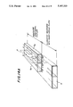
FIGS. 13A and 13B are respectively plan and front views of a phase inverter according to a third embodiment of the present invention. The illustrated phase inverter uses waveguide directional couplers arranged as shown in FIG. 12. Waveguide directional couplers 801, 802, 803 and 804 are of the magnetic field coupling type and correspond to the waveguide directional couplers 701, 702, 703 and 704, respectively. A broken line represents an inner wall. Three-branch waveguides 811, 812, 813 and 814 are arranged into a ring and couple the waveguide directional couplers 801 -804, which extend radially. An elongated waveguide 82 having a length of λ0 /4 (λ0 is the wavelength within the waveguide 82) is directly connected to an end of the waveguide directional coupler 804. Short- circuit plates 831, 832, 833 are provided for ends of the waveguide directional couplers 801, 802 and 803, respectively, so that the main and couple ports thereof are short-circuited. A short-circuit plate 834 is provided for an end of the elongated waveguide 82 so that main and couple ports thereof are short-circuited. No short-circuit plate is fastened to the end of the waveguide directional coupler 804. Terminals 841, 842, 843 and 844 are connected to the three-branch waveguides 811, 812, 813 and 814, respectively.
Each of the waveguide directional couplers 801 -804 has a structure as shown in FIG. 14A. The one-dotted chain lines shown in FIG. 14A represent the elongated waveguide 82 shown in FIG. 13A. Each of the waveguide directional couplers 801 -804 has an input port A, a main port B, a couple port C and an isolation port D. As illustrated by the arrows, a signal input through the input port A is output through the main port B and the couple port C. Signals which are respectively input through the main port and the coupled port C are combined and then drawn through the isolation port D. A letter "S" indicates the short-circuit plate 834 (a short-circuit plate provided for the end of the waveguide directional coupler is omitted for the sake of simplicity), a reference GM indicate a main guide, and a reference GA indicates an auxiliary guide, and a reference "P" indicates a plane of symmetry of magnetic field.
Turning to FIG. 13A, a signal supplied to the terminal 841 (Δ) is equally distributed so that 180° out-of-phase signals are output from the terminals 842 (P1) and 844 (P2). No signal is output from the terminal 843 (Σ). Alternatively, 180° out-of-phase signals supplied to the terminals 842 (P1) and 844 (P2) are combined so that a signal is output from the terminal 841 (Δ). The short-circuit plate 831 is directly connected to the waveguide directional coupler 801. Alternatively, a short-circuit element of a waveguide having a length l equal to (λ0 /4)n and a short-circuit plate connected to an end thereof may be used where `n` is an integer. When n=0, the short-circuit plate 831 is directly connected to the end of the waveguide directional coupler 801. When the short-circuit element of a length l equal to (λ0 /4)n is used, the elongated waveguide 82 having a length of λ0 /4 is replaced by an elongated waveguide having a length l' of (λ0 /4)(n+1) and having a short-circuit plate connected to an end thereof. In this alternative, there is a 180° phase difference between the path between the input port A and the isolation port D of the waveguide directional coupler 801 and the path between the input port A and the isolation port D of the waveguide directional coupler 804. A signal applied to the elongated waveguide 82 is reflected by the short-circuit plate 834 and is then output therefrom so that a phase difference of (λ0 /4)×2=180° can be generated.
Alternatively, each of the waveguide directional couplers 701 -704 (FIG.12) may be formed by an electric field coupling type waveguide directional coupler as shown in FIG.14B, in which those parts which have the same functions as those in FIG.14A are given the same reference numbers. The waveguide directional coupler shown in FIG.14A has two waveguides arranged side by side. On the other hand, the waveguide directional coupler shown in FIG. 14B has waveguides elevationally stacked.
FIG. 15A is diagram showing the type of each of the waveguide directional couplers shown in FIGS. 13A and 13B. Each of the waveguide directional couplers 801, 802 and 803 is of the double-end grounded type, and the combination of the waveguide directional coupler 804 and the elongated waveguide 82 having the short-circuit plate 834 (elongated waveguide short-circuit element) is of the double-end open type. Alternatively, as shown in FIG. 15B, it is possible to employ three waveguide directional couplers of the double-end open type and a waveguide directional coupler of the double-end grounded type. In the alternative, a λ0 /4 elongated waveguide having a short-circuit plate is directly connected to an end of each of the waveguide directional coupler of the double-end open type, and a short-circuit plate is directly connected to an end of the remaining waveguide directional plate of the double-end grounded type. It can be seen from the above description that the third embodiment of the present invention has four variations. The first and second variations are phase inverters having the arrangement shown in FIG.15A in which the waveguide directional couplers are of the magnetic field coupling type and the electric field coupling type. The third and fourth variations are phase inverters having the arrangement shown in FIG. 15B in which the waveguide directional couplers are of the magnetic field coupling type and the electric field coupling type.
FIG. 16 is a circuit diagram of a push-pull amplifier which uses two phase inverters according to the present invention. The illustrated push-pull amplifier has two phase inverters 90 and 91 configured according to the present invention. The phase inverter 90 has a single input terminal and two output terminals, and the phase inverter 91 has two input terminals and a single output terminal. An amplifier A1 is provided between one of the two output terminals of the phase inverter 90 and one of the two input terminals of the phase inverter 91. An amplifier A2 is provided between the other output terminal of the phase inverter 90 and the other input terminal of the phase inverter 91. An RF (radio frequency) signal a is applied to the phase inverter 90, which outputs two output signals b and c having a phase difference of 180°. The signals b and c are amplified by the amplifiers A1 and A2, respectively, and supplied to the phase inverter 91. The amplified signals b and c are combined by the phase inverter 91, which generates an RF output signal d. The amplifiers A1 and A2 are B-class amplifiers. Thus, each of the amplifiers A1 and A2 amplifies either one of the polarities of the amplified signals b and c. The phase of amplified signal b is inverted by 180° by the phase inverter 91 so that the RF output signal d has both the polarities. The phase inverters 90 and 91 have middle-point ground terminals 92 and 93, respectively so that the reference D.C. level of the output signal b is equal to that of the output signal c.
FIG. 17 is a diagram of a push-pull amplifier in which the phase inverters 90 and 91 are formed by λ/4 parallel coupled line networks according to the first embodiment of the present invention. Each of the phase inverters has one grounded-coupled line network between the terminals 21 and 23. Thus, it is considered that a middle-point ground terminal is substantially provided between the networks provided between the terminals 21 and 23. The terminal 22 of the phase inverter 90 which is grounded through a resistor R1 (having a resistance of 50 ohms, for example) corresponds to the middle-point ground terminal 92 shown in FIG.16. The terminal 22 of the phase inverter 91 which is grounded through a resistor R2 (having a resistance of 50 ohms, for example) corresponds to the middle-point ground terminal 93 shown in FIG.16. An RF signal is applied to the terminal 20 of the phase inverter 90. The B-class amplifier A1 is connected between the terminal 21 of the phase inverter 90 and the terminal 23 of the phase inverter 91. The B-class amplifier A2 is connected between the terminal 23 of the phase inverter 90 and the terminal 21 of the phase inverter 91. The RF output signal is drawn from the terminal 20 of the phase inverter 91.
FIG. 18 is a diagram of a push-pull amplifier in which the phase inverters 90 and 91 are formed by directional couplers according to the second embodiment of the present invention. An RF input signal is applied to the terminal 30 of the phase inverter 90, which outputs 180° out-of-phase signals through the terminals 31 and 33. The signals drawn from the terminals 31 and 33 pass through the B-class amplifier A1 and A2, and then are applied to the terminals 33 and 31 of the phase inverter 91, respectively. The RF signal is drawn from the terminal 30 the phase inverter 91. The terminals 32 of the phase inverters 90 and 91 are grounded through the resistors R1 and R2, respectively. The terminals 32 of the phase inverters 90 and 91 correspond to the middle-point ground terminals 92, and 93, respectively.
FIG. 19 is a diagram of a push-pull amplifier in which the phase inverters 90 and 91 are formed by waveguide directional couplers according to the third embodiment of the present invention. An RF input signal is applied to one of the three branches of the three-branch waveguide 841 of the phase inverter 90. One of the three branches of the three-branch waveguide 842 is coupled to the B-class amplifier A1 through a waveguide 861. One of the three branches of the three-branch waveguides 844 of the phase inverter 90 is coupled to the B-class amplifier A2 through a waveguide 863. A non-reflection terminator 85 having a resistance of 50 ohms is connected to one of the three branches of the three-branch waveguide 843 of the phase inverter 90. The B-class amplifier A1 is connected to one of the three branches of the three-branch waveguide 844 of the phase inverter 91 through a waveguide 862, and the B-class amplifier A2 is connected to one of the three-branches of the three-branch waveguide 842 of the phase inverter 91 through a waveguide 864. A non-reflection terminator 87 having a resistance of 50 ohms is connected to the one of the three branches of the three-branch waveguide 843 of the phase inverter 91. The short-circuit elements 731, 732, 733 and 734 (FIG.12) serving as the middle-point ground terminals 92 and 93 (FIG. 16) are provided so that the reference D.C. level of the output signal b is equal to that of the output signal c.
The present invention is applied to not only the push-pull amplifier but also a mixer, a mono-pulse comparator and the like.
The present invention is not limited to the aforementioned embodiments, and variations and modifications may be made without departing from the scope of the present invention.