US5090609A - Method of bonding metals, and method and apparatus for producing semiconductor integrated circuit device using said method of bonding metals - Google Patents
Method of bonding metals, and method and apparatus for producing semiconductor integrated circuit device using said method of bonding metals Download PDFInfo
- Publication number
- US5090609A US5090609A US07/514,943 US51494390A US5090609A US 5090609 A US5090609 A US 5090609A US 51494390 A US51494390 A US 51494390A US 5090609 A US5090609 A US 5090609A
- Authority
- US
- United States
- Prior art keywords
- bonding
- eutectic alloy
- metal members
- semiconductor chip
- substrate
- Prior art date
- Legal status (The legal status is an assumption and is not a legal conclusion. Google has not performed a legal analysis and makes no representation as to the accuracy of the status listed.)
- Expired - Lifetime
Links
Images


Classifications
-
- H—ELECTRICITY
- H01—ELECTRIC ELEMENTS
- H01L—SEMICONDUCTOR DEVICES NOT COVERED BY CLASS H10
- H01L24/00—Arrangements for connecting or disconnecting semiconductor or solid-state bodies; Methods or apparatus related thereto
- H01L24/80—Methods for connecting semiconductor or other solid state bodies using means for bonding being attached to, or being formed on, the surface to be connected
- H01L24/81—Methods for connecting semiconductor or other solid state bodies using means for bonding being attached to, or being formed on, the surface to be connected using a bump connector
-
- H—ELECTRICITY
- H01—ELECTRIC ELEMENTS
- H01L—SEMICONDUCTOR DEVICES NOT COVERED BY CLASS H10
- H01L21/00—Processes or apparatus adapted for the manufacture or treatment of semiconductor or solid state devices or of parts thereof
- H01L21/02—Manufacture or treatment of semiconductor devices or of parts thereof
- H01L21/04—Manufacture or treatment of semiconductor devices or of parts thereof the devices having at least one potential-jump barrier or surface barrier, e.g. PN junction, depletion layer or carrier concentration layer
- H01L21/48—Manufacture or treatment of parts, e.g. containers, prior to assembly of the devices, using processes not provided for in a single one of the subgroups H01L21/06 - H01L21/326
- H01L21/4814—Conductive parts
- H01L21/4846—Leads on or in insulating or insulated substrates, e.g. metallisation
- H01L21/4853—Connection or disconnection of other leads to or from a metallisation, e.g. pins, wires, bumps
-
- H—ELECTRICITY
- H01—ELECTRIC ELEMENTS
- H01L—SEMICONDUCTOR DEVICES NOT COVERED BY CLASS H10
- H01L23/00—Details of semiconductor or other solid state devices
- H01L23/02—Containers; Seals
- H01L23/04—Containers; Seals characterised by the shape of the container or parts, e.g. caps, walls
- H01L23/053—Containers; Seals characterised by the shape of the container or parts, e.g. caps, walls the container being a hollow construction and having an insulating or insulated base as a mounting for the semiconductor body
- H01L23/055—Containers; Seals characterised by the shape of the container or parts, e.g. caps, walls the container being a hollow construction and having an insulating or insulated base as a mounting for the semiconductor body the leads having a passage through the base
-
- H—ELECTRICITY
- H01—ELECTRIC ELEMENTS
- H01L—SEMICONDUCTOR DEVICES NOT COVERED BY CLASS H10
- H01L23/00—Details of semiconductor or other solid state devices
- H01L23/48—Arrangements for conducting electric current to or from the solid state body in operation, e.g. leads, terminal arrangements ; Selection of materials therefor
- H01L23/488—Arrangements for conducting electric current to or from the solid state body in operation, e.g. leads, terminal arrangements ; Selection of materials therefor consisting of soldered or bonded constructions
- H01L23/498—Leads, i.e. metallisations or lead-frames on insulating substrates, e.g. chip carriers
- H01L23/49811—Additional leads joined to the metallisation on the insulating substrate, e.g. pins, bumps, wires, flat leads
- H01L23/49816—Spherical bumps on the substrate for external connection, e.g. ball grid arrays [BGA]
-
- H—ELECTRICITY
- H05—ELECTRIC TECHNIQUES NOT OTHERWISE PROVIDED FOR
- H05K—PRINTED CIRCUITS; CASINGS OR CONSTRUCTIONAL DETAILS OF ELECTRIC APPARATUS; MANUFACTURE OF ASSEMBLAGES OF ELECTRICAL COMPONENTS
- H05K3/00—Apparatus or processes for manufacturing printed circuits
- H05K3/30—Assembling printed circuits with electric components, e.g. with resistor
- H05K3/32—Assembling printed circuits with electric components, e.g. with resistor electrically connecting electric components or wires to printed circuits
- H05K3/34—Assembling printed circuits with electric components, e.g. with resistor electrically connecting electric components or wires to printed circuits by soldering
- H05K3/3457—Solder materials or compositions; Methods of application thereof
- H05K3/3478—Applying solder preforms; Transferring prefabricated solder patterns
-
- H—ELECTRICITY
- H01—ELECTRIC ELEMENTS
- H01L—SEMICONDUCTOR DEVICES NOT COVERED BY CLASS H10
- H01L2224/00—Indexing scheme for arrangements for connecting or disconnecting semiconductor or solid-state bodies and methods related thereto as covered by H01L24/00
- H01L2224/01—Means for bonding being attached to, or being formed on, the surface to be connected, e.g. chip-to-package, die-attach, "first-level" interconnects; Manufacturing methods related thereto
- H01L2224/10—Bump connectors; Manufacturing methods related thereto
- H01L2224/11—Manufacturing methods
- H01L2224/11001—Involving a temporary auxiliary member not forming part of the manufacturing apparatus, e.g. removable or sacrificial coating, film or substrate
- H01L2224/11003—Involving a temporary auxiliary member not forming part of the manufacturing apparatus, e.g. removable or sacrificial coating, film or substrate for holding or transferring the bump preform
-
- H—ELECTRICITY
- H01—ELECTRIC ELEMENTS
- H01L—SEMICONDUCTOR DEVICES NOT COVERED BY CLASS H10
- H01L2224/00—Indexing scheme for arrangements for connecting or disconnecting semiconductor or solid-state bodies and methods related thereto as covered by H01L24/00
- H01L2224/01—Means for bonding being attached to, or being formed on, the surface to be connected, e.g. chip-to-package, die-attach, "first-level" interconnects; Manufacturing methods related thereto
- H01L2224/10—Bump connectors; Manufacturing methods related thereto
- H01L2224/11—Manufacturing methods
- H01L2224/113—Manufacturing methods by local deposition of the material of the bump connector
- H01L2224/1133—Manufacturing methods by local deposition of the material of the bump connector in solid form
- H01L2224/11334—Manufacturing methods by local deposition of the material of the bump connector in solid form using preformed bumps
-
- H—ELECTRICITY
- H01—ELECTRIC ELEMENTS
- H01L—SEMICONDUCTOR DEVICES NOT COVERED BY CLASS H10
- H01L2224/00—Indexing scheme for arrangements for connecting or disconnecting semiconductor or solid-state bodies and methods related thereto as covered by H01L24/00
- H01L2224/01—Means for bonding being attached to, or being formed on, the surface to be connected, e.g. chip-to-package, die-attach, "first-level" interconnects; Manufacturing methods related thereto
- H01L2224/10—Bump connectors; Manufacturing methods related thereto
- H01L2224/12—Structure, shape, material or disposition of the bump connectors prior to the connecting process
- H01L2224/13—Structure, shape, material or disposition of the bump connectors prior to the connecting process of an individual bump connector
- H01L2224/13001—Core members of the bump connector
- H01L2224/13099—Material
- H01L2224/131—Material with a principal constituent of the material being a metal or a metalloid, e.g. boron [B], silicon [Si], germanium [Ge], arsenic [As], antimony [Sb], tellurium [Te] and polonium [Po], and alloys thereof
- H01L2224/13101—Material with a principal constituent of the material being a metal or a metalloid, e.g. boron [B], silicon [Si], germanium [Ge], arsenic [As], antimony [Sb], tellurium [Te] and polonium [Po], and alloys thereof the principal constituent melting at a temperature of less than 400°C
- H01L2224/13111—Tin [Sn] as principal constituent
-
- H—ELECTRICITY
- H01—ELECTRIC ELEMENTS
- H01L—SEMICONDUCTOR DEVICES NOT COVERED BY CLASS H10
- H01L2224/00—Indexing scheme for arrangements for connecting or disconnecting semiconductor or solid-state bodies and methods related thereto as covered by H01L24/00
- H01L2224/01—Means for bonding being attached to, or being formed on, the surface to be connected, e.g. chip-to-package, die-attach, "first-level" interconnects; Manufacturing methods related thereto
- H01L2224/10—Bump connectors; Manufacturing methods related thereto
- H01L2224/12—Structure, shape, material or disposition of the bump connectors prior to the connecting process
- H01L2224/13—Structure, shape, material or disposition of the bump connectors prior to the connecting process of an individual bump connector
- H01L2224/1354—Coating
- H01L2224/13599—Material
- H01L2224/136—Material with a principal constituent of the material being a metal or a metalloid, e.g. boron [B], silicon [Si], germanium [Ge], arsenic [As], antimony [Sb], tellurium [Te] and polonium [Po], and alloys thereof
-
- H—ELECTRICITY
- H01—ELECTRIC ELEMENTS
- H01L—SEMICONDUCTOR DEVICES NOT COVERED BY CLASS H10
- H01L2224/00—Indexing scheme for arrangements for connecting or disconnecting semiconductor or solid-state bodies and methods related thereto as covered by H01L24/00
- H01L2224/01—Means for bonding being attached to, or being formed on, the surface to be connected, e.g. chip-to-package, die-attach, "first-level" interconnects; Manufacturing methods related thereto
- H01L2224/10—Bump connectors; Manufacturing methods related thereto
- H01L2224/15—Structure, shape, material or disposition of the bump connectors after the connecting process
- H01L2224/16—Structure, shape, material or disposition of the bump connectors after the connecting process of an individual bump connector
-
- H—ELECTRICITY
- H01—ELECTRIC ELEMENTS
- H01L—SEMICONDUCTOR DEVICES NOT COVERED BY CLASS H10
- H01L2224/00—Indexing scheme for arrangements for connecting or disconnecting semiconductor or solid-state bodies and methods related thereto as covered by H01L24/00
- H01L2224/73—Means for bonding being of different types provided for in two or more of groups H01L2224/10, H01L2224/18, H01L2224/26, H01L2224/34, H01L2224/42, H01L2224/50, H01L2224/63, H01L2224/71
- H01L2224/732—Location after the connecting process
- H01L2224/73251—Location after the connecting process on different surfaces
- H01L2224/73253—Bump and layer connectors
-
- H—ELECTRICITY
- H01—ELECTRIC ELEMENTS
- H01L—SEMICONDUCTOR DEVICES NOT COVERED BY CLASS H10
- H01L2224/00—Indexing scheme for arrangements for connecting or disconnecting semiconductor or solid-state bodies and methods related thereto as covered by H01L24/00
- H01L2224/80—Methods for connecting semiconductor or other solid state bodies using means for bonding being attached to, or being formed on, the surface to be connected
- H01L2224/81—Methods for connecting semiconductor or other solid state bodies using means for bonding being attached to, or being formed on, the surface to be connected using a bump connector
- H01L2224/81009—Pre-treatment of the bump connector or the bonding area
- H01L2224/8101—Cleaning the bump connector, e.g. oxide removal step, desmearing
- H01L2224/81012—Mechanical cleaning, e.g. abrasion using hydro blasting, brushes, ultrasonic cleaning, dry ice blasting, gas-flow
-
- H—ELECTRICITY
- H01—ELECTRIC ELEMENTS
- H01L—SEMICONDUCTOR DEVICES NOT COVERED BY CLASS H10
- H01L2224/00—Indexing scheme for arrangements for connecting or disconnecting semiconductor or solid-state bodies and methods related thereto as covered by H01L24/00
- H01L2224/80—Methods for connecting semiconductor or other solid state bodies using means for bonding being attached to, or being formed on, the surface to be connected
- H01L2224/81—Methods for connecting semiconductor or other solid state bodies using means for bonding being attached to, or being formed on, the surface to be connected using a bump connector
- H01L2224/818—Bonding techniques
- H01L2224/81801—Soldering or alloying
-
- H—ELECTRICITY
- H01—ELECTRIC ELEMENTS
- H01L—SEMICONDUCTOR DEVICES NOT COVERED BY CLASS H10
- H01L2924/00—Indexing scheme for arrangements or methods for connecting or disconnecting semiconductor or solid-state bodies as covered by H01L24/00
- H01L2924/01—Chemical elements
- H01L2924/01005—Boron [B]
-
- H—ELECTRICITY
- H01—ELECTRIC ELEMENTS
- H01L—SEMICONDUCTOR DEVICES NOT COVERED BY CLASS H10
- H01L2924/00—Indexing scheme for arrangements or methods for connecting or disconnecting semiconductor or solid-state bodies as covered by H01L24/00
- H01L2924/01—Chemical elements
- H01L2924/01006—Carbon [C]
-
- H—ELECTRICITY
- H01—ELECTRIC ELEMENTS
- H01L—SEMICONDUCTOR DEVICES NOT COVERED BY CLASS H10
- H01L2924/00—Indexing scheme for arrangements or methods for connecting or disconnecting semiconductor or solid-state bodies as covered by H01L24/00
- H01L2924/01—Chemical elements
- H01L2924/01013—Aluminum [Al]
-
- H—ELECTRICITY
- H01—ELECTRIC ELEMENTS
- H01L—SEMICONDUCTOR DEVICES NOT COVERED BY CLASS H10
- H01L2924/00—Indexing scheme for arrangements or methods for connecting or disconnecting semiconductor or solid-state bodies as covered by H01L24/00
- H01L2924/01—Chemical elements
- H01L2924/01024—Chromium [Cr]
-
- H—ELECTRICITY
- H01—ELECTRIC ELEMENTS
- H01L—SEMICONDUCTOR DEVICES NOT COVERED BY CLASS H10
- H01L2924/00—Indexing scheme for arrangements or methods for connecting or disconnecting semiconductor or solid-state bodies as covered by H01L24/00
- H01L2924/01—Chemical elements
- H01L2924/01029—Copper [Cu]
-
- H—ELECTRICITY
- H01—ELECTRIC ELEMENTS
- H01L—SEMICONDUCTOR DEVICES NOT COVERED BY CLASS H10
- H01L2924/00—Indexing scheme for arrangements or methods for connecting or disconnecting semiconductor or solid-state bodies as covered by H01L24/00
- H01L2924/01—Chemical elements
- H01L2924/01033—Arsenic [As]
-
- H—ELECTRICITY
- H01—ELECTRIC ELEMENTS
- H01L—SEMICONDUCTOR DEVICES NOT COVERED BY CLASS H10
- H01L2924/00—Indexing scheme for arrangements or methods for connecting or disconnecting semiconductor or solid-state bodies as covered by H01L24/00
- H01L2924/01—Chemical elements
- H01L2924/01047—Silver [Ag]
-
- H—ELECTRICITY
- H01—ELECTRIC ELEMENTS
- H01L—SEMICONDUCTOR DEVICES NOT COVERED BY CLASS H10
- H01L2924/00—Indexing scheme for arrangements or methods for connecting or disconnecting semiconductor or solid-state bodies as covered by H01L24/00
- H01L2924/01—Chemical elements
- H01L2924/0105—Tin [Sn]
-
- H—ELECTRICITY
- H01—ELECTRIC ELEMENTS
- H01L—SEMICONDUCTOR DEVICES NOT COVERED BY CLASS H10
- H01L2924/00—Indexing scheme for arrangements or methods for connecting or disconnecting semiconductor or solid-state bodies as covered by H01L24/00
- H01L2924/01—Chemical elements
- H01L2924/01072—Hafnium [Hf]
-
- H—ELECTRICITY
- H01—ELECTRIC ELEMENTS
- H01L—SEMICONDUCTOR DEVICES NOT COVERED BY CLASS H10
- H01L2924/00—Indexing scheme for arrangements or methods for connecting or disconnecting semiconductor or solid-state bodies as covered by H01L24/00
- H01L2924/01—Chemical elements
- H01L2924/01074—Tungsten [W]
-
- H—ELECTRICITY
- H01—ELECTRIC ELEMENTS
- H01L—SEMICONDUCTOR DEVICES NOT COVERED BY CLASS H10
- H01L2924/00—Indexing scheme for arrangements or methods for connecting or disconnecting semiconductor or solid-state bodies as covered by H01L24/00
- H01L2924/01—Chemical elements
- H01L2924/01075—Rhenium [Re]
-
- H—ELECTRICITY
- H01—ELECTRIC ELEMENTS
- H01L—SEMICONDUCTOR DEVICES NOT COVERED BY CLASS H10
- H01L2924/00—Indexing scheme for arrangements or methods for connecting or disconnecting semiconductor or solid-state bodies as covered by H01L24/00
- H01L2924/01—Chemical elements
- H01L2924/01078—Platinum [Pt]
-
- H—ELECTRICITY
- H01—ELECTRIC ELEMENTS
- H01L—SEMICONDUCTOR DEVICES NOT COVERED BY CLASS H10
- H01L2924/00—Indexing scheme for arrangements or methods for connecting or disconnecting semiconductor or solid-state bodies as covered by H01L24/00
- H01L2924/01—Chemical elements
- H01L2924/01079—Gold [Au]
-
- H—ELECTRICITY
- H01—ELECTRIC ELEMENTS
- H01L—SEMICONDUCTOR DEVICES NOT COVERED BY CLASS H10
- H01L2924/00—Indexing scheme for arrangements or methods for connecting or disconnecting semiconductor or solid-state bodies as covered by H01L24/00
- H01L2924/01—Chemical elements
- H01L2924/01082—Lead [Pb]
-
- H—ELECTRICITY
- H01—ELECTRIC ELEMENTS
- H01L—SEMICONDUCTOR DEVICES NOT COVERED BY CLASS H10
- H01L2924/00—Indexing scheme for arrangements or methods for connecting or disconnecting semiconductor or solid-state bodies as covered by H01L24/00
- H01L2924/013—Alloys
- H01L2924/0132—Binary Alloys
- H01L2924/01322—Eutectic Alloys, i.e. obtained by a liquid transforming into two solid phases
-
- H—ELECTRICITY
- H01—ELECTRIC ELEMENTS
- H01L—SEMICONDUCTOR DEVICES NOT COVERED BY CLASS H10
- H01L2924/00—Indexing scheme for arrangements or methods for connecting or disconnecting semiconductor or solid-state bodies as covered by H01L24/00
- H01L2924/013—Alloys
- H01L2924/014—Solder alloys
-
- H—ELECTRICITY
- H01—ELECTRIC ELEMENTS
- H01L—SEMICONDUCTOR DEVICES NOT COVERED BY CLASS H10
- H01L2924/00—Indexing scheme for arrangements or methods for connecting or disconnecting semiconductor or solid-state bodies as covered by H01L24/00
- H01L2924/095—Indexing scheme for arrangements or methods for connecting or disconnecting semiconductor or solid-state bodies as covered by H01L24/00 with a principal constituent of the material being a combination of two or more materials provided in the groups H01L2924/013 - H01L2924/0715
- H01L2924/097—Glass-ceramics, e.g. devitrified glass
- H01L2924/09701—Low temperature co-fired ceramic [LTCC]
-
- H—ELECTRICITY
- H01—ELECTRIC ELEMENTS
- H01L—SEMICONDUCTOR DEVICES NOT COVERED BY CLASS H10
- H01L2924/00—Indexing scheme for arrangements or methods for connecting or disconnecting semiconductor or solid-state bodies as covered by H01L24/00
- H01L2924/10—Details of semiconductor or other solid state devices to be connected
- H01L2924/11—Device type
- H01L2924/12—Passive devices, e.g. 2 terminal devices
- H01L2924/1204—Optical Diode
- H01L2924/12042—LASER
-
- H—ELECTRICITY
- H01—ELECTRIC ELEMENTS
- H01L—SEMICONDUCTOR DEVICES NOT COVERED BY CLASS H10
- H01L2924/00—Indexing scheme for arrangements or methods for connecting or disconnecting semiconductor or solid-state bodies as covered by H01L24/00
- H01L2924/10—Details of semiconductor or other solid state devices to be connected
- H01L2924/11—Device type
- H01L2924/14—Integrated circuits
-
- H—ELECTRICITY
- H01—ELECTRIC ELEMENTS
- H01L—SEMICONDUCTOR DEVICES NOT COVERED BY CLASS H10
- H01L2924/00—Indexing scheme for arrangements or methods for connecting or disconnecting semiconductor or solid-state bodies as covered by H01L24/00
- H01L2924/15—Details of package parts other than the semiconductor or other solid state devices to be connected
- H01L2924/151—Die mounting substrate
- H01L2924/1517—Multilayer substrate
- H01L2924/15172—Fan-out arrangement of the internal vias
- H01L2924/15174—Fan-out arrangement of the internal vias in different layers of the multilayer substrate
-
- H—ELECTRICITY
- H01—ELECTRIC ELEMENTS
- H01L—SEMICONDUCTOR DEVICES NOT COVERED BY CLASS H10
- H01L2924/00—Indexing scheme for arrangements or methods for connecting or disconnecting semiconductor or solid-state bodies as covered by H01L24/00
- H01L2924/15—Details of package parts other than the semiconductor or other solid state devices to be connected
- H01L2924/151—Die mounting substrate
- H01L2924/153—Connection portion
- H01L2924/1531—Connection portion the connection portion being formed only on the surface of the substrate opposite to the die mounting surface
- H01L2924/15311—Connection portion the connection portion being formed only on the surface of the substrate opposite to the die mounting surface being a ball array, e.g. BGA
-
- H—ELECTRICITY
- H01—ELECTRIC ELEMENTS
- H01L—SEMICONDUCTOR DEVICES NOT COVERED BY CLASS H10
- H01L2924/00—Indexing scheme for arrangements or methods for connecting or disconnecting semiconductor or solid-state bodies as covered by H01L24/00
- H01L2924/15—Details of package parts other than the semiconductor or other solid state devices to be connected
- H01L2924/161—Cap
- H01L2924/1615—Shape
- H01L2924/16152—Cap comprising a cavity for hosting the device, e.g. U-shaped cap
-
- H—ELECTRICITY
- H01—ELECTRIC ELEMENTS
- H01L—SEMICONDUCTOR DEVICES NOT COVERED BY CLASS H10
- H01L2924/00—Indexing scheme for arrangements or methods for connecting or disconnecting semiconductor or solid-state bodies as covered by H01L24/00
- H01L2924/15—Details of package parts other than the semiconductor or other solid state devices to be connected
- H01L2924/161—Cap
- H01L2924/166—Material
-
- H—ELECTRICITY
- H05—ELECTRIC TECHNIQUES NOT OTHERWISE PROVIDED FOR
- H05K—PRINTED CIRCUITS; CASINGS OR CONSTRUCTIONAL DETAILS OF ELECTRIC APPARATUS; MANUFACTURE OF ASSEMBLAGES OF ELECTRICAL COMPONENTS
- H05K2203/00—Indexing scheme relating to apparatus or processes for manufacturing printed circuits covered by H05K3/00
- H05K2203/01—Tools for processing; Objects used during processing
- H05K2203/0104—Tools for processing; Objects used during processing for patterning or coating
- H05K2203/0113—Female die used for patterning or transferring, e.g. temporary substrate having recessed pattern
-
- H—ELECTRICITY
- H05—ELECTRIC TECHNIQUES NOT OTHERWISE PROVIDED FOR
- H05K—PRINTED CIRCUITS; CASINGS OR CONSTRUCTIONAL DETAILS OF ELECTRIC APPARATUS; MANUFACTURE OF ASSEMBLAGES OF ELECTRICAL COMPONENTS
- H05K2203/00—Indexing scheme relating to apparatus or processes for manufacturing printed circuits covered by H05K3/00
- H05K2203/01—Tools for processing; Objects used during processing
- H05K2203/0147—Carriers and holders
- H05K2203/016—Temporary inorganic, non-metallic carrier, e.g. for processing or transferring
-
- H—ELECTRICITY
- H05—ELECTRIC TECHNIQUES NOT OTHERWISE PROVIDED FOR
- H05K—PRINTED CIRCUITS; CASINGS OR CONSTRUCTIONAL DETAILS OF ELECTRIC APPARATUS; MANUFACTURE OF ASSEMBLAGES OF ELECTRICAL COMPONENTS
- H05K2203/00—Indexing scheme relating to apparatus or processes for manufacturing printed circuits covered by H05K3/00
- H05K2203/03—Metal processing
- H05K2203/0338—Transferring metal or conductive material other than a circuit pattern, e.g. bump, solder, printed component
-
- H—ELECTRICITY
- H05—ELECTRIC TECHNIQUES NOT OTHERWISE PROVIDED FOR
- H05K—PRINTED CIRCUITS; CASINGS OR CONSTRUCTIONAL DETAILS OF ELECTRIC APPARATUS; MANUFACTURE OF ASSEMBLAGES OF ELECTRICAL COMPONENTS
- H05K2203/00—Indexing scheme relating to apparatus or processes for manufacturing printed circuits covered by H05K3/00
- H05K2203/04—Soldering or other types of metallurgic bonding
- H05K2203/041—Solder preforms in the shape of solder balls
-
- H—ELECTRICITY
- H05—ELECTRIC TECHNIQUES NOT OTHERWISE PROVIDED FOR
- H05K—PRINTED CIRCUITS; CASINGS OR CONSTRUCTIONAL DETAILS OF ELECTRIC APPARATUS; MANUFACTURE OF ASSEMBLAGES OF ELECTRICAL COMPONENTS
- H05K3/00—Apparatus or processes for manufacturing printed circuits
- H05K3/30—Assembling printed circuits with electric components, e.g. with resistor
- H05K3/32—Assembling printed circuits with electric components, e.g. with resistor electrically connecting electric components or wires to printed circuits
- H05K3/34—Assembling printed circuits with electric components, e.g. with resistor electrically connecting electric components or wires to printed circuits by soldering
- H05K3/3489—Composition of fluxes; Methods of application thereof; Other methods of activating the contact surfaces
Definitions
- This invention relates to a method of bonding metals and to a technique for fabricating a semiconductor integrated circuit device using the method, which technique is effective when applied to a semiconductor integrated circuit device based on, for instance, the flip-chip system or TAB (Tape Automated Bonding) system.
- the number of terminals (input/output pins) for connection to external circuits has recently been rapidly increasing due to the increases in the number of functions and the packaging density of integrated circuits.
- the wire bonding system in which connection of a semiconductor chip to external circuits is effected through wires bonded to bonding pads provided at the peripheral portions of the chip, has therefore been reaching the limit of application thereof.
- the wire bonding system has drawbacks in that the need for the wiring in an internal circuit region to be laid around to the bonding pads in the peripheral regions leads to a larger wiring length, resulting in a delay in signal transmission rate.
- the wire bonding system is thus unsuitable for mounting a logic LSI which requires high-speed operations.
- the flip chip system in which a semiconductor chip is mounted on a substrate through CCB bumps (projected electrodes) provided on Al electrodes of the chip by use of a solder material, and to the TAB system in which bumps comprising an Au-Sn eutectic alloy are provided on the Al electrodes and the semiconductor chip is mounted through the bumps onto leads provided on a principal surface of an insulation film.
- the flip chip system is an extremely effective mounting system for an increase in the number of pins of the semiconductor chip because the system makes it possible to provide terminals not only in the peripheral areas of the semiconductor chip but on the entire surface of the chip, namely, also in the internal circuit region of the chip. With the terminals provided in the internal circuit region, moreover, the wiring length is reduced, which makes the flip chip system extremely effective for use as a system for mounting a high-speed LSI.
- the CCB bumps are provided as follows. First, thin films comprising Cr, Cu and Au, for instance, are sequentially vapor deposited on the Al electrodes of the semiconductor chip to provide a soldering primary coat (BLM: Bump Limiting Metallization).
- BBM Bump Limiting Metallization
- solder film comprising a pb-Sn alloy or the like is selectively vapor deposited on the soldering primary coat, and the solder film is melted by heating in a melting furnace filed with an inert gas atmosphere, to form spherical CCB bumps by utilizing the surface tension of the solder film thus melted.
- the solder ball supply method is a method in which contaminants such as oxides, moisture, oils and fats, etc., deposited on the surfaces of the Al electrodes are removed completely by ion impacts and then spherical solder balls are superposed on the cleaned surfaces in an ultra high vacuum, followed by bonding, as for instance described on pages 88-91 of "Yosetsu Gijutsu (Welding Technology)" issued in July, 1987.
- a chip carrier is one of the semiconductor integrated circuit devices based on the above-mentioned flip chip system.
- the chip carrier is described in, for instance, Japanese Patent Application Laid-Open (KOKAI) Nos. 62-249429 (1987) and 63-310139 (1988).
- FIG. 15 shows a sectional structure of a chip carrier described in the above-mentioned literature.
- the chip carrier 50 has a packaged structure in which a semiconductor chip 54 connected through CCB bumps 53 to electrodes 52 provided on a principal surface of a package substrate 51 comprising a ceramic material, such as mullite, is hermetically sealed (or encapsulated) by a cap 55.
- the cap 55 comprises, for instance, aluminum nitride (AlN) and is bonded to the principal surface of the package substrate 51 through a sealing solder 56.
- AlN aluminum nitride
- the back side (upper surface) of the semiconductor chip 54 is bonded to a lower surface of the cap 55 through a heat-transmitting solder 57, in order that the heat generated from the chip 54 is transmitted through the solder 57 to the cap 55.
- Electrodes 52 on the lower surface of the package substrate 51 are provided thereon with CCB bumps 58 for mounting the chip carrier 50 on a module substrate or the like.
- the CCB bumps 58 are bonded to the electrodes 52 by, for instance, the solder ball supply method, after fabrication of the chip carrier 50 is completed.
- the package substrate 51 is provided therein with an internal wiring 59 comprising W (tungsten), for instance, through which the electrodes 52, 52 on the principal surface and the lower surface of the package substrate 51 are electrically connected.
- the CCB bumps of the semiconductor chip are positioned accurately on the electrodes on the principal surface of the package substrate by a chip mounting device.
- a flux is applied to bonding portions of the CCB bumps and the electrodes.
- the flux is applied for removal of natural oxide films formed on the surfaces of the solder constituting the CCB bumps and for preventing the re-oxidation of the solder surfaces at the time of reflow.
- a further purpose of flux application is to enhance the wettability by solder at the time of reflow.
- the package substrate is transferred into a reflow furnace. It is necessary, in this transfer, to prevent the slippage of the CCB bumps due to vibration or the like.
- the flux serves also for the prevention of the slippage.
- the reflow furnace is provided therein with an inert gas atmosphere, in which the CCB bumps are re melted by heating, whereby the semiconductor chip is bonded, with its face side down, to the principal surface of the package substrate (namely, facedown bonding is effected).
- the cap is soldered to the principal surface of the package substrate by the sealing solder.
- the back side of the semiconductor chip is soldered to the lower surface of the cap by the heat-transmitting solder.
- the soldering of the cap to the principal surface of the package substrate is carried out by preliminarily depositing a sealing preliminary solder on the principal surface of the package substrate and base portions of the cap, applying a flux to the surfaces of the preliminary solder, then placing the cap on the principal surface of the package substrate, and re-melting the preliminary solder by heating in the reflow furnace.
- the soldering of the back side of the semiconductor chip to the lower surface of the cap is carried out by preliminarily depositing a heat-transmitting preliminary solder on the lower surface of the cap or on the back side of the semiconductor chip, applying a flux to the surface of the preliminary solder, and then re melting the preliminary solder by heating in the reflow furnace.
- the sealing solder and the heat-transmitting solder therefore, comprise solder materials having approximately equal melting temperatures.
- the melting temperatures of the sealing solder and the heat-transmitting solder are lower than the melting point of the solder constituting the CCB bumps; otherwise, the CCB bumps would be re-melted at the time of re meting the preliminary solders by heating in the reflow furnace, and the CCB bumps would collapse under the load of the cap, leading to short circuit between adjacent ones of the CCB bumps.
- the acceptability of the soldering affects greatly the reliability of connection of the CCB bumps, the reliability of hermetic seal (or encapsulation) of the package and the cooling efficiency.
- the TAB system and the flip chip system as mentioned above involve the following problems.
- the TAB system has been pointed out to have the problem of the increased manufacturing cost of TAB packages due to the formation of expensive Au-containing bumps on the Al electrodes of the semiconductor chip.
- the flip chip system has the following problems.
- a step of cleaning a flux is required after the reflow step, and the number of mounting steps is increased accordingly.
- a cleaning liquid such as a chlorohydrocarbon, a fluorohydrocarbon, etc.
- the flux cleaning step has been becoming controlled, from the viewpoint of protection of natural environments. In view of this, it is urgently demanded to eliminate the flux cleaning step.
- a method of producing a flip chip package according to one invention in this application is a method for facedown bonding of a semiconductor chip to a substrate through CCB bumps, which comprises first placing the semiconductor chip and the substrate into a vacuum vessel, irradiating the surfaces of the CCB bumps and the surfaces of electrodes on the substrate with an atomic or ion energy beam to clean bonding surfaces, then transferring the semiconductor chip and the substrate into a vessel filled with a high-purity inert gas atmosphere, pressing the CCB bumps against the electrodes under normal pressure (about 1 atm) to effect temporary bonding, and effecting the reflow of the CCB bumps to achieve the desired bonding.
- a single gas or mixed gas having an oil and fat content and an oxygen content of not more than 10 ppb each, a moisture content of not more than 100 ppb, and a dew point of not higher than -70° C.
- a method of producing a flip chip package according to another invention in this application is a facedown bonding method in which CCB bumps provided by use of a non eutectic solder are melted and then immediately cooled rapidly, whereby a eutectic solder layer or a solder layer close in composition to the eutectic solder layer is preliminarily segregated to the surface of the non-eutectic solder, followed by the same procedure as in the method according to the one invention mentioned above.
- a method of producing a TAB package according to a further invention in this application is a method for gang bonding of a semiconductor chip through bumps to leads provided on a principal surface of an insulation film, which comprises first placing the semiconductor chip and the insulation film into a vacuum vessel, irradiating the surfaces of the bumps and the surfaces of the leads with an atomic or ion energy beam, then immediately transferring the semiconductor chip and the insulation film into a vessel filled with a high-purity inert gas atmosphere, and pressing the leads against the bumps in the vessel to achieve the desired bonding.
- a method of bonding metals according to yet another invention in this application comprises irradiating bonding surfaces of a pair of metal members placed in a vacuum vessel with an atomic or ion energy beam, then transferring the metal members into a vessel filled with a high-purity inert gas atmosphere, and pressing the bonding surfaces against each other under norma pressure.
- the pressing of the bonding surfaces against each other may be accompanied by heating the metal members at a temperature not higher than the melting temperatures of the members.
- a metal softer than the metals to be bonded may be preliminarily provided on the surface of at least one of the metal members so as to utilize a plastic deformation of the softer metal for the intended bonding. In that case, for lowering the bonding pressure required, the bonding portions may be heated to lower the yield point of the softer metal.
- the eutectic solder layer or the solder layer close in composition to the eutectic solder layer is preliminarily segregated to the surfaces of the CCB bumps comprising a eutectic solder, whereby it is possible to effect the reflow of the solder at a temperature in the vicinity of the eutectic point of the solder (about 183° C.) and, therefore, to further reduce the heat damage to the semiconductor chip. It is also possible, by the method, to further promote shortening of the reflow time and reduction in the capacity of a reflow furnace.
- the method of producing a TAB package according to the further invention in this application enables formation of the bumps by use of a metallic material less expensive than Au, thereby enabling a reduction in the manufacturing cost of the TAB package.
- heating of the metals to be bonded makes the metals themselves softer, whereby adhesion of bonding surfaces is enhanced.
- a metal softer than the metals to be bonded is preliminarily provided on the bonding surfaces, it is possible to enhance the adhesion of the bonding surfaces easily through utilization of a plastic deformation of the softer metal.
- FIG. 1 is a flow diagram illustrating the process for fabricating a semiconductor integrated circuit device according to one embodiment of this invention
- FIG. 2 is a schematic perspective view of an apparatus for fabricating the semiconductor integrated circuit device, used in the embodiment
- FIGS. 3 and 4 are each a sectional view of a semiconductor chip, illustrating a CCB bump forming step in the embodiment
- FIGS. 5(a) to 5(c) are each a partial front view of a temporary bonding mechanism in the apparatus used in the embodiment;
- FIG. 6 is a partial perspective view of a temporary bonding mechanism in the apparatus used in the embodiment.
- FIGS. 7 and 8 are each a sectional view of a semiconductor chip and a package substrate, illustrating a facedown bonding step in the embodiment
- FIG. 9 is a sectional view of a cap, illustrating a preliminary solder forming step in the embodiment.
- FIG. 10 is a sectional view of the semiconductor chip and the package substrate, illustrating a preliminary solder forming step in the embodiment
- FIGS. 11 and 12 are each a sectional view of a chip carrier, illustrating a hermetic sealing step (encapsulating step) in the embodiment;
- FIG. 13 is a partial sectional view of a glass jig, illustrating the CCB bump forming step in the embodiment
- FIG. 14 (a) is a sectional view of a chip carrier produced by the embodiment
- FIG. 14 (b) is an enlarged partial view of a package seal portion in the chip carrier
- FIG. 15 is a sectional view of a conventional chip carrier.
- FIG. 16 is a sectional view of an important portion for illustrating a process for fabricating a semiconductor integrated circuit device according to another embodiment of this invention.
- FIG. 14 (a) shows a sectional structure of a chip carrier 1 obtained by the method according to this embodiment.
- the chip carrier 1 has a packaged structure in which a semiconductor chip 5 facedown bonded to electrodes 4 on a principal surface of a package substrate 3 through CCB bumps 2 is encapsulated (or hermetically sealed) by a cap 6.
- the cap 6 is soldered to the principal surface of the package substrate 3 through a sealing solder 7, and the back side of the semiconductor chip 5 is soldered to the lower surface of the cap 6 through a heat transmitting solder 8.
- CCB bumps 9 greater in diameter than the above CCB bumps 2 are bonded.
- the CCB bumps 9 are electrically connected to the CCB bumps 2 through an internal wiring 10 comprising W (tungsten) or the like, and further to the semiconductor chip 5.
- the CCB bumps 9 serve as external terminals at the time of mounting the chip carrier 1 on a module substrate, and are bonded to the electrodes 4 on the lower side of the package substrate 3 after completion of the step of encapsulating (hermetically sealing) the chip carrier 1.
- a soldering metallization layer (primary metal coat) 11 is provided, as required, on a peripheral portion of the principal surface of the package substrate 3 and on a base portion of the cap 6, as shown in FIG. 14 (b).
- the soldering metallization layer 11 comprises a composite metallic film in which, for instance, a chromium (Cr), titanium (Ti) or tungsten (W) film 11a, a copper Cu), nickel (Ni) or platinum (Pt) film 11b and a gold (Au) film 11c are provided in layers.
- a soldering metallization layer 11 comprising the composite metallic film is provided also on the lower surface of the cap 6, as required.
- the soldering metallization layers 11 are provided primarily for enhancing the wettability by the sealing solder 7 and the heat-transmitting solder 8.
- the package substrate 3 comprises a ceramic material such as mullite (3Al 2 O 3 ⁇ 2SiO 2 ), whereas the cap 6 comprises, for instance, aluminum nitride (AlN) or silicon carbide (SiC).
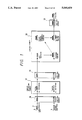
- FIG. 2 shows an important portion of an apparatus 12 used for the step of fabricating the above-mentioned chip carrier 1.
- the apparatus 12 comprises loading magazines 14a and 14b provided at one end (on this side of the figure) of a base 13 of the apparatus.
- One of the loading magazines, 14a contains a multiplicity of chip trays 15a, each of which carries a predetermined number of semiconductor chips 5 placed thereon.
- Each of the semiconductor chips 15 is placed in the condition where the side on which CCB bumps 2 are provided is directed up.
- the other loading magazine 14b contains a multiplicity of substrate trays 15b, each of which carries a predetermined number of package substrates 3 placed thereon. Each of the package substrate 3 is placed, with its principal surface up.
- the trays 15a and 15b contained in the loading magazines 14a and 14b are first transferred into a surface activation chamber 17 through a first load-lock chamber 16.
- the surface activation chamber 17 is so designed to be capable of being evacuated to a vacuum degree of up to 10 -6 Torr.
- the surface activation chamber 17 is provided with a pair of source guns 18, 18 for converting an Ar gas introduced therein into an atomic beam.
- the atomic beam is used to irradiate the semiconductor chips 5 and the package substrates 3 therewith to perform a surface activation treatment of the CCB bumps 2 and the electrodes 4, as described later.
- the semiconductor chips 5 and the package substrates 3 are immediately transferred into a bonding chamber 10 through a second load-lock chamber 19, in the state of being contained respectively in the trays 15a and 15b.
- the bonding chamber 20 is provided therein with a high-purity inert gas atmosphere at normal pressure (about 1 atm).
- the high-purity inert gas atmosphere supplied from gas supplying means provided in the bonding chamber, is a nitrogen, Ar or other similar inert gas atmosphere from which moisture oil and fat components and oxygen have been removed chemically through a gas cleaner or the like.
- the bonding chamber 20 is provided therein with a temporay bonding mechanism which comprises a chip inversion stage 21, a chip inversion unit 22, a chip mounting hand 23, a temporay bonding stage 24, a prism mirror 25, a position recognition camera 26, etc., and with a fusion bonding mechanism which comprises a fusion bonding stage 27, a heat bock 28, a chip transfer hand 29, an aligning stage 30, etc. These mechanisms are used to perform the temporary bonding and permanent bonding, which will be described later.
- the package substrates 3 with the semiconductor chips 5 facedown-bonded thereto are placed on the substrate tray 15b, to be contained into an unloading magazine 37 through a third load-lock chamber 31.
- a solder film 40 is provided selectively on each electrode 4 of the semiconductor chip by, for example, a solder vapor deposition method.
- the electrodes 4 of the semiconductor chip 5 comprise Al, and a soldering primary coat comprising a composite metallic film of Cr, Cu and Au is vapor deposited on the surfaces of the electrodes 4.
- the solder film 40 is melted by heating in a melting furnace filled with a nitrogen, Ar or other similar inert gas atmosphere, to provide spherical CCB bumps 2 through utilization of the surface tension of the solder upon melting.
- the CCB bumps 2 thus melted are rapidly cooled, whereby a thin eutectic solder layer comprising a eutectic Pb-Sn alloy with an Sn content of 60% by weight (or a solder layer with a composition close to the eutectic solder composition) 41 is segregated to the surfaces of the CCB bumps 2, as shown in FIG. 4.
- the melting point (eutectic point) of the eutectic solder layer 4 is about 183° C., which is much lower than the melting temperature of the non-eutectic Pb-Sn alloy constituting the inside layer of the CCB bumps 2.
- a predetermined number of the semiconductor chips 5 are paced on the chip tray 15a, and are contained into the loading magazine 14a of the apparatus 12. Also, a predetermined number of the package substrates 3 are placed on the substrate tray 15b, and are contained into the loading magazine 14b.
- one chip tray 15a and one substrate tray 15b are transferred into the load-lock chamber 16, which is once evacuated to a vacuum degree of about 10 -6 Torr, and then the chip tray 15a and the substrate tray 15b are transferred into the surface activation chamber 17.
- the surface activation chamber 17 is evacuated beforehand to a vacuum degree of about 10 -6 Torr. Subsequently, a high-purity Ar gas with a moisture content of 100 ppb or below and a dew point of -70° C.
- the surface activation chamber 17 or below is supplied into the surface activation chamber 17, to a vacuum degree of about 10 -3 to 10 -4 Torr, and the source guns 18 are operated to irradiate the semiconductor chips 5 and the package substrates 3 with Ar atomic beams for about 5 minutes.
- the source guns 18 are operated to irradiate the semiconductor chips 5 and the package substrates 3 with Ar atomic beams for about 5 minutes.
- the trays 15a and 15b are transferred from the surface activation chamber 17 into the second load-lock chamber 19.
- the load-lock chamber 19 is evacuated beforehand to a vacuum degree of about 10 -3 to 10 -4 Torr.
- a high-purity nitrogen gas (or Ar gas) is supplied into the load-lock chamber 19 to once provide normal pressure (about 1 atm) inside the chamber.
- the trays 15a and 15b are transferred into the bonding chamber 20, in which the chip tray 15a is placed on the chip inversion stage 21, and the substrate tray 15b on the temporary bonding stage 24.
- the bonding chamber 20 is supplied beforehand with the high-purity nitrogen gas (or Ar gas) to obtain normal pressure.
- the high-purity gas to be supplied into the bonding chamber 20 may be, for example, a reducing gas obtained by adding about 10 to 20% of a hydrogen gas to a nitrogen gas.
- the semiconductor chips 5 and the package substrates 3 are immediately transferred into the bonding chamber 20 filed with the high-purity inert gas atmosphere.
- the fabrication of the chip carrier is carried out in a continuous apparatus, thereby preventing the re-formation of natural oxide films or re deposition of foreign matter on the surfaces of the CCB bumps 2 or the surfaces of the electrodes 4 during the transfer from the surface activation chamber 17 into the bonding chamber 20.
- a plunge-up pin 32 embedded in the chip inversion stage 21 is raised from the back side of the chip tray 15a to lift up one of the semiconductor chips 5.
- the semiconductor chip 5 is attracted by suction onto the lower end of a collet 33 kept waiting on the upper side of the chip 5.
- the collet 33 is inverted, or turned 180°, and the semiconductor chip 5 is sucked onto the lower end of a chip mounting hand 23 kept waiting on the upper side of the collet 33, whereby the chip 5 is transferred onto the temporary bonding stage 24.
- the semiconductor chip 5 is heated by a heater (not shown) incorporated in the chip mounting hand 23.
- the heating is carried out at a temperature (e.g., 150° C.) sightly lower than the melting point (183° C.) of the eutectic solder.
- a predetermined number of package substrates 3 placed on the substrate tray 15b are set waiting on the temporary bonding stage 24.
- the chip mounting hand 23 with the semiconductor chip 5 held thereon by suction is stopped at a position on the upper side of the temporary bonding stage 24.
- the image of the semiconductor chip 5 projected on a prism mirror 25 is detected by the position recognition camera 26, and a precision XY table 34, a high-speed XY table 35 and a turntable 36 are driven to match the positions of the CCB bumps 2 accurately to the positions of the corresponding electrodes 24.
- the chip mounting hand 23 is lowered to press the CCB bumps 2 against the electrodes 4 for about 10 seconds, under a load of about 0.5 kgf/cm 2 on the back side of the semiconductor chip 5.
- This causes the CCB bumps 2, preliminarily heated to the temperature slightly lower than the melting point of the eutectic solder, to be plastically deformed easily and be temporarily bonded to the electrodes 4.
- the semiconductor chip 5 temporarily bonded to the principal surface of the package substrate 3 as above is again held by suction onto the chip mounting hand 23, and is transferred onto the fusion bonding stage 27 together with the package substrate 3.
- the slippage between the CCB bumps 2 and the corresponding electrodes 4 is prevented from occurring due to vibration or the like during the transfer.
- the heat block 28 disposed on the upper side of the fusion bonding stage 27 is lowered to heat the semiconductor chip 5 while exerting a load of about 0.5-5 kgf/cm 2 on the back side of the chip 5.
- the heating is carried out at a temperature (e.g., 200° C.) sightly higher than the melting point (183° C.) of the eutectic solder.
- the thin eutectic solder layer 41 preliminarily segregated to the surface of each CCB bump 2 is melted and caused to diffuse into the CCB bump and into the electrode 4, whereby the CCB bump 2 and the corresponding electrode 4 are bonded firmly to each other.
- the application of the load to the back side of the semiconductor chip 5 enhances the wettability by the melted eutectic solder layer 41.
- the chip 5 is sucked by the chip transfer hand 29, and is transferred together with the substrate 3 onto an aligning stage 30, to be paced on the substrate tray 15a.
- the substrate tray 15a is contained into the unloading magazine 37 through the third load-lock chamber 31, whereby the facedown bonding step is competed.
- the semiconductor chips 5 and the package substrates 3 are first irradiated with Ar atomic beams in the evacuated surface activation chamber 17, whereby natural oxide films and foreign matter are removed from the surfaces of the CCB bumps 2 and the surfaces of the electrodes 4.
- the semiconductor chip 5 and the package substrate 3 are immediately transferred into the bonding chamber 20 filled with the high-purity inert gas atmosphere, thereby preventing the re-formation of natural oxide films or re- deposition of foreign matter on the surfaces of the CCB bumps 2 or the surfaces of the electrodes 4 from occurring during the transfer from the surface activation chamber 17 into the bonding chamber 20.
- the CCB bumps 2 are temporarily bonded to the electrodes 4 so as to achieve perfect contact of the bumps 2 with the electrodes 4, whereby failure in connection between the CCB bumps 2 and the corresponding electrodes 4 is prevented from occurring due to diameter dispersion of the bumps 2 or warpage of the package substrate 3.
- the package substrate 3 (with the semiconductor chip 5 temporarily bonded to the principal surface thereof) is transferred onto the fusion bonding stage 27, thereby preventing the slippage between the CCB bumps 2 and the corresponding electrodes 4 due to vibration or the like during the transfer.
- the eutectic solder layer 41 preliminarily segregated to the surface of each CCB bump 2 is caused to diffuse into the bump 2 and into the corresponding electrode 4, thereby bonding the bump 2 and the electrode 4 to each other.
- the facedown bonding step makes it possible to reduce markedly the heat damage to the semiconductor chip, to complete the facedown bonding in a shorter time, and to use a smaller apparatus, as compared with the prior art in which facedown bonding is performed by effecting reflow of CCB bumps in a reflow furnace set at a temperature considerably higher than the melting temperature of a non-eutectic solder.
- a sealing preliminary solder 7a and a heat-transmitting preliminary solder 8a are deposited on the surfaces of the soldering metallization layers 11 provided on the cap 6.
- the preliminary solders 7a and 8a are deposited by placing solder preforms (not shown) of predetermined shapes on the soldering metallization layers 11, and melting the solder preforms by heating in a melting furnace filed with a nitrogen, Ar or other similar inert gas atmosphere.
- the sealing preliminary solder 7a and the heat-transmitting preliminary solder 8a may be deposited on the surfaces of the soldering metallization layers 11 on the package substrate 3 and on the back side of the semiconductor chip 5 after completion of the facedown bonding, as illustrated in FIG. 10. Further, the preliminary solders 7a and 8a may be deposited on both the cap 6 and the package substrate 3. The following explanation will be made of the case where the preliminary solders 7a and 8a are deposited only on the cap 6 (FIG. 9).
- a predetermined number of the caps 6 are placed on an exclusive cap tray (not shown), to be contained into the loading magazine 14a of the apparatus 12.
- a predetermined number of the package substrates 3, for which the facedown bonding step is finished, are placed on the substrate tray 15b, to be contained into the loading magazine 14b.
- one cap tray and one substrate tray 15b are transferred through the load-lock chamber 16 into the surface activation chamber 17.
- the source guns 18 are operated in a high-purity Ar gas atmosphere of about 10 -3 to 10 -4 . Torr, thereby irradiating the principal surfaces of the package substrates 3 and the caps 6 uniformly with Ar atomic beams.
- the irradiation with the Ar atomic beams removes natural oxide films and foreign matter from the surfaces of the preliminary solders 7a and 8a, thereby activating the surfaces.
- natural oxide films and foreign matter are removed from the surfaces of the soldering metallization layers 11 provided on the principal surfaces of the package substrates 3, whereby the surfaces are activated.
- the cap tray and the substrate tray 15b are transferred through the second load-lock chamber 19 into the bonding chamber 20 provided therein with a high-purity nitrogen gas (or Ar gas) atmosphere namely, a normal-pressure condition), in which the cap tray is placed on the chip inversion stage 21, and the substrate tray 15b on the temporary bonding stage 24.
- a high-purity nitrogen gas or Ar gas
- the cap 6 is inverted, or turned 180°, by use of the plung-up pin 32 and the collet 33, the inverted cap 6 is transferred onto the temporary bonding stage 24 by the chip transfer hand 23.
- the cap 6 is heated by a heater incorporated in the chip transfer hand 23.
- the heating is performed at a temperature (e.g., 250° C.) slightly lower than the melting temperatures of the preliminary solders 7a and 8a.
- a temperature e.g. 250° C.
- the surfaces of the CCB bumps 2 cannot be re melted, because the above-mentioned eutectic solder layer 41 segregated to the surfaces of the CCB bumps 2 is completely diffused into the bumps 2 and the electrodes 4 in the above-mentioned facedown bonding step.
- the position of the cap 6 projected on the prism mirror 25 shown in FIG. 6 is detected by the position recognition camera 26, and the precision XY table 34, high speed XY table 35 and turntable 36 are driven to position one package substrate 3 right under the cap 6.
- the temporary bonding prevents the slippage between the cap 6 and the package substrate 3 from occurring due to vibration or the like at the time of transferring the package substrate 3 (with the cap 6 temporarily bonded to the principal surface thereof) onto the fusion bonding stage 27.
- the heat block 28 is lowered, as shown in FIG. 12, to heat the cap 6 while exerting a load of about 0.5 to 5 kgf/cm 2 on the upper surface of the cap 6.
- the heating is carried out at a temperature (e.g., 310° C.) slightly higher than the melting temperatures of the preliminary solders 7a and 8a.
- the application of the load to the upper surface of the cap 6 enhances the wettability by the preliminary solders 7a and 8a.
- the CCB bumps 2 cannot be re-melted when the preliminary solders 7a and 8a are melted, because the melting temperature of the CCB bumps 2 is about 320° to 330° C.
- the cap 6 After the semiconductor chip 5 is hermetically sealed (or encapsulated) by the cap 6 as above, the cap 6 is sucked by the chip transfer hand 29, and is transferred together with the package substrate 3 onto the aligning stage 30, to be cooled to room temperature. After the cooling, the packages semiconductor chips 5 are contained into the unloading magazine 37 through the third load-lock chamber 3, whereby the hermetic sealing (encapsulating) step is completed and the chip carriers 1 are finished.
- the hermetic sealing (encapsulating) step it is possible to hermetically seal (encapsulate) the semiconductor chip 5 at a temperature near the melting temperatures of the preliminary solders 7a and 8a.
- the hermetic sealing step therefore, makes it possible to reduce markedly the heat damage to the semiconductor chip, and to complete the hermetic sealing in a shorter time, as compared with the prior art in which the hermetic sealing (encapsulation) is conducted by effecting the reflow of the preliminary solders 7a and 8a in a reflow furnace set at a temperature considerably higher than the melting points of the solders 7a and 8a.
- solder balls 9a are supplied to the principal surface of the glass jig 43 provided with a multiplicity of holes 42, thereby fitting one solder ball 9a in each of the holes 42.
- the number and positions of the holes 42 correspond respectively to the number and positions of the electrodes 4 provided on the lower side of the package substrate 3.
- a predetermined number of the glass jigs 43 are placed on an exclusive tray (not shown), to be contained into the loading magazine 14a of the apparatus 12.
- a predetermined number of the chip carriers 1 are placed on the substrate tray 15b, to be contained into the loading magazine 14b.
- the chip carriers 1 are each placed in the condition where the lower side thereof (the side on which the electrodes 4 for bonding the CCB bump 9 thereto are provided) is directed upward.
- the glass jigs 43 and the chip carriers 2 are transferred into the surface activation chamber 17 through the load-lock chamber 16 shown in FIGS. 1 and 2, and the solder balls 9 and the electrodes 4 are irradiated with Ar atomic beams to remove natural oxide films and foreign matter from the surfaces of the solder balls 9 and the electrodes 4.
- the glass jigs 43 and the chip carriers 1 are transferred through the load-lock chamber 19 into the bonding chamber 20, in which the chip carrier 1 is inverted, or turned 180°, and the electrodes 4 are pressed against the solder balls 9a to effect temporary bonding.
- the temporary bonding is carried out at a temperature (e.g., 150° C.) slightly lower than the melting temperature of the solder balls 9a.
- the chip carriers 1 are transferred onto the fusion bonding stage 27, where the solder balls 9a are heated at a temperature (e.g., 250° C.) slightly higher than the melting temperature thereof. By the heating, the solder balls 9a are melted and the CCB bumps 9 are bonded to the electrodes 4 (FIG. 14(a)).
- a temperature e.g. 250° C.
- the bump bonding step it is possible to bond the CCB bumps 9 to the electrodes 14 on the lower side of the package substrate 3, at a temperature near the melting point of the solder balls 9a and in a short time.
- fabrication of the chip carrier 1 is carried out by use of the above-mentioned apparatus 12 in which the vacuum surface activation chamber 17 provided with the source guns for generating Ar atomic beams and the bonding chamber 20 equipped with the temporary bonding mechanism and the fusion bonding mechanism and filed with the high-purity inert gas atmosphere are connected to each other through the load-lock chamber 19, whereby it is possible to perform favorable soldering in each of the steps, without use of flux.
- a metal softer than the metals to be bonded may be provided beforehand on a bonding surface of at least one of the CCB bump and the corresponding electrode so as to give the bonding surface an ultra-smooth finish, thereby contriving close contact of the bonding surfaces through utilizing a plastic deformation of the softer metal.
- the bonding portions may be heated to lower the yield point of the softer metal, for the purpose of reducing the bonding pressure required.
- the softer metal may be, for example, Sn.
- the invention is applicable a)so to a step of mounting the chip carrier on a module substrate through the CCB bumps.
- this invention is applicable to a method of fabricating a so-called multi-tip package in which a plurality of semiconductor chips facedown-bonded to the principal surface of a package substrate are hermetically sealed (or encapsulated) by a cap.
- this invention is applicable not only to a method of producing a flip chip but to a method of producing a TAB package, as shown in FIG. 16.
- a semiconductor chip 60 is gang-bonded through bumps 63 to leads 62 provided on a principal surface of an insulation film 61 as follows.
- a soldering primary coat comprising a composite metallic film of, for example, Cr, Cu and Au is vapor deposited on the surfaces of Al electrodes 64 of a semiconductor chip 60.
- solder bumps 63 are provided on the electrodes by a solder vapor deposition method or a solder ball supply method.
- solder bumps 63 are then immediately cooled rapidly, whereby a eutectic solder layer (or a solder layer with a composition close to the eutectic solder composition) is segregated to the surfaces of the bumps 63. Then, the semiconductor chip 60 and the insulation film 61 are contained into a vacuum vessel such as the above-mentioned surface treatment chamber, in which the surfaces of the solder bumps 63 and the surfaces of the leads 62 are irradiated with Ar atomic beams to remove oxide films and foreign matter from the surfaces.
- a vacuum vessel such as the above-mentioned surface treatment chamber
- the semiconductor chip 60 and the insulation film 61 are transferred into a vessel filled with a high-purity inert gas atmosphere, and the leads 62 are pressed against the solder bumps 63 in the vessel, thereby achieving the gang bonding.
- a method of fabricating a semiconductor integrated circuit device comprises, in facedown bonding of a semiconductor chip to a substrate through CCB bumps, the steps of placing the semiconductor chip and the substrate into a vacuum vessel, irradiating the surfaces of the CCB bumps and the surfaces of electrodes on the substrate with an atomic or ion energy beam, then immediately transferring the semiconductor chip and the substrate into a vessel filled with a high-purity inert gas atmosphere, pressing the CCB bumps against the electrodes under normal pressure to effect temporary bonding, and thereafter effecting reflow of the CCB bump.
- This method makes it possible to effect the reflow of the CCB bumps at a temperature near the melting temperature of the bumps and, therefore, to reduce the heat damage to the semiconductor chip. It is also possible to realize shortening of the reflow time and a reduction in the capacity of a reflow furnace required.
- the method of fabricating a semiconductor integrated circuit device eliminates the need for use of a flux in the facedown bonding of the semiconductor chip to the substrate through the CCB bumps. Therefore, the need for a flux application step and the need for a flux cleaning step are eliminated, and the number of steps for facedown bonding is reduced accordingly. It is also possible, by the method according to this invention, to obviate the corrosion of wiring in an integrated circuit due to a flux residue. It is further possible, by the method, to prevent defects in solder bond portions from being generated due to the flux residue so that the reliability of connection of the CCB bumps is enhanced.
- a method of fabricating a semiconductor device comprises providing the CCB bumps by use of a non-eutectic solder, melting the non-eutectic solder and then immediately cooling the melted non eutectic solder rapidly to cause segregation of a eutectic solder layer or a solder layer close in composition to the eutectic solder layer to the surfaces of the CCB bumps, prior to facedown bonding in the same manner as in the invention relevant to the above description (I).
- This method makes it possible to effect the reflow of the CCB bumps at a further lower temperature and to further reduce the heat damage to the semiconductor chip, as compared with the invention relevant to the above description (I).
- a method of fabricating a semiconductor integrated circuit device comprises, in fabricating a TAB package by gang bonding of a semiconductor chip through bumps to leads provided on a principal surface of an insulation film, the steps of pacing the semiconductor chip and the insulation film into a vacuum vessel, irradiating the surfaces of the bumps and the surfaces of the leads with an atomic or ion energy beam, then immediately transferring the semiconductor chip and the insulation film into a vessel filled with a high-purity inert gas atmosphere, and pressing the leads against the bumps in the vessel filled with the inert gas atmosphere to effect the gang bonding.
- This method makes it possible to provide the bumps by use of a metallic material less expensive than Au and, therefore, to reduce the manufacturing cost of the TAB package.
Abstract
Description
Claims (24)
Priority Applications (1)
| Application Number | Priority Date | Filing Date | Title |
|---|---|---|---|
| US07/812,024 US5188280A (en) | 1989-04-28 | 1991-12-23 | Method of bonding metals, and method and apparatus for producing semiconductor integrated circuit device using said method of bonding metals |
Applications Claiming Priority (6)
| Application Number | Priority Date | Filing Date | Title |
|---|---|---|---|
| JP10764989 | 1989-04-28 | ||
| JP1-107649 | 1989-04-28 | ||
| JP1123353A JPH02303676A (en) | 1989-05-17 | 1989-05-17 | Joining method by brazing material and treating device as well as semiconductor device |
| JP1-123353 | 1989-05-17 | ||
| JP1-309922 | 1989-11-29 | ||
| JP1309922A JP2786700B2 (en) | 1989-11-29 | 1989-11-29 | Method and apparatus for manufacturing semiconductor integrated circuit device |
Related Child Applications (1)
| Application Number | Title | Priority Date | Filing Date |
|---|---|---|---|
| US07/812,024 Continuation US5188280A (en) | 1989-04-28 | 1991-12-23 | Method of bonding metals, and method and apparatus for producing semiconductor integrated circuit device using said method of bonding metals |
Publications (1)
| Publication Number | Publication Date |
|---|---|
| US5090609A true US5090609A (en) | 1992-02-25 |
Family
ID=27311042
Family Applications (1)
| Application Number | Title | Priority Date | Filing Date |
|---|---|---|---|
| US07/514,943 Expired - Lifetime US5090609A (en) | 1989-04-28 | 1990-04-26 | Method of bonding metals, and method and apparatus for producing semiconductor integrated circuit device using said method of bonding metals |
Country Status (1)
| Country | Link |
|---|---|
| US (1) | US5090609A (en) |
Cited By (58)
| Publication number | Priority date | Publication date | Assignee | Title |
|---|---|---|---|---|
| US5186381A (en) * | 1991-04-16 | 1993-02-16 | Samsung Electronics, Co., Ltd. | Semiconductor chip bonding process |
| US5188280A (en) * | 1989-04-28 | 1993-02-23 | Hitachi Ltd. | Method of bonding metals, and method and apparatus for producing semiconductor integrated circuit device using said method of bonding metals |
| US5193738A (en) * | 1992-09-18 | 1993-03-16 | Microfab Technologies, Inc. | Methods and apparatus for soldering without using flux |
| US5280414A (en) * | 1990-06-11 | 1994-01-18 | International Business Machines Corp. | Au-Sn transient liquid bonding in high performance laminates |
| DE4235908A1 (en) * | 1992-10-23 | 1994-04-28 | Telefunken Microelectron | Method for soldering a semiconductor body to a carrier element |
| EP0604005A1 (en) * | 1992-10-26 | 1994-06-29 | Texas Instruments Incorporated | Device packaged in a high interconnect density land grid array package having electrical and optical interconnects |
| US5346857A (en) * | 1992-09-28 | 1994-09-13 | Motorola, Inc. | Method for forming a flip-chip bond from a gold-tin eutectic |
| US5359767A (en) * | 1993-08-26 | 1994-11-01 | International Business Machines Corporation | Method of making multilayered circuit board |
| EP0625796A2 (en) * | 1993-05-18 | 1994-11-23 | Hitachi, Ltd. | Soldering method and apparatus for use in connecting electronic circuit devices |
| US5523622A (en) * | 1992-11-24 | 1996-06-04 | Hitachi, Ltd. | Semiconductor integrated device having parallel signal lines |
| EP0718882A1 (en) * | 1993-09-03 | 1996-06-26 | Advanced Semiconductor Assembly Technology, Inc. | Tab grid array for a semiconductor device |
| EP0684641A3 (en) * | 1994-05-26 | 1996-11-06 | Nec Corp | Semiconductor device moulding capable of accomplishing a high moisture proof. |
| US5579985A (en) * | 1993-07-26 | 1996-12-03 | Kabushiki Kaisha Shinkawa | Chip bonding method and apparatus |
| WO1997020654A1 (en) * | 1995-12-01 | 1997-06-12 | Fraunhofer-Gesellschaft zur Förderung der angewandten Forschung e.V. | Process and device for applying a solder to a substrate or chip without flux |
| WO1997022138A2 (en) * | 1995-12-09 | 1997-06-19 | Robert Bosch Gmbh | Flip-chip process for producing a multi-chip module |
| US5671530A (en) * | 1995-10-30 | 1997-09-30 | Delco Electronics Corporation | Flip-chip mounting assembly and method with vertical wafer feeder |
| US5707684A (en) * | 1994-02-28 | 1998-01-13 | Microfab Technologies, Inc. | Method for producing micro-optical components |
| US5722581A (en) * | 1995-06-09 | 1998-03-03 | L'air Liquide, Societe Anonyme Pour L'etude Et L'exploitation Des Procedes George Claude | Method and device for wave soldering incorporating a dry fluxing operation |
| US5729440A (en) * | 1995-05-25 | 1998-03-17 | International Business Machines Corporation | Solder hierarchy for chip attachment to substrates |
| US5732706A (en) * | 1996-03-22 | 1998-03-31 | Lockheed Martin Ir Imaging Systems, Inc. | Ultrasonic array with attenuating electrical interconnects |
| US5801446A (en) * | 1995-03-28 | 1998-09-01 | Tessera, Inc. | Microelectronic connections with solid core joining units |
| NL1006366C2 (en) * | 1997-06-20 | 1998-12-22 | Meco Equip Eng | Method and device for bonding solder balls to a substrate. |
| US5941448A (en) * | 1996-06-07 | 1999-08-24 | L'air Liquide, Societe Anonyme Pour L'etude Et L'exploitation Des Procedes Georges Claude | Method for dry fluxing of metallic surfaces, before soldering or tinning, using an atmosphere which includes water vapor |
| US5965944A (en) * | 1997-11-12 | 1999-10-12 | International Business Machines Corporation | Printed circuit boards for mounting a semiconductor integrated circuit die |
| US5968389A (en) * | 1996-03-15 | 1999-10-19 | Commissariat A L'energie Atomique | Method and machine for hybridization by refusion |
| US6130476A (en) * | 1994-01-31 | 2000-10-10 | International Business Machines Corporation | Semiconductor chip package having chip-to-carrier mechanical/electrical connection formed via solid state diffusion |
| US6133633A (en) * | 1996-10-31 | 2000-10-17 | International Business Machines Corporation | Method for building interconnect structures by injection molded solder and structures built |
| US6152353A (en) * | 1999-01-14 | 2000-11-28 | Celestica International Inc. | Printed circuit board header attachment station |
| US6168971B1 (en) | 1998-05-05 | 2001-01-02 | Fujitsu Limited | Method of assembling thin film jumper connectors to a substrate |
| US6197612B1 (en) * | 1997-10-23 | 2001-03-06 | Nec Corporation | Semiconductor chip mounting apparatus capable of preventing connected portion between semiconductor chip and substrate from thermal stress and method thereof |
| US6210546B1 (en) | 1998-10-29 | 2001-04-03 | Lucent Technologies Inc. | Fixture with at least one trough and method of using the fixture in a plasma or ion beam |
| US20010049875A1 (en) * | 2000-02-25 | 2001-12-13 | Shinji Watanabe | Size reduction of chip mounting system |
| WO2002015258A1 (en) * | 2000-08-04 | 2002-02-21 | Toray Engineering Co., Ltd. | Mounting method |
| WO2002017378A1 (en) * | 2000-08-18 | 2002-02-28 | Toray Engineering Co., Ltd. | Mounting method and device |
| US6399902B1 (en) | 2000-08-01 | 2002-06-04 | Advanced Micro Devices, Inc. | Inline flux measurement system |
| US6410881B2 (en) * | 1995-05-19 | 2002-06-25 | Hitachi, Ltd. | Process for manufacturing electronic circuits |
| US6575351B1 (en) * | 1999-06-18 | 2003-06-10 | Shibuya Kogyo Co., Ltd. | Work/head positioning apparatus for ball mount apparatus |
| US6642068B1 (en) | 2002-05-03 | 2003-11-04 | Donald J. Hayes | Method for producing a fiber optic switch |
| US6666371B2 (en) * | 2001-05-22 | 2003-12-23 | Fujitsu Media Devices Limited | Sealing system for electronic device and sealing method therefor |
| WO2004030079A1 (en) * | 2002-09-26 | 2004-04-08 | Toray Engineering Co., Ltd. | Connection method and connection device |
| US20040180468A1 (en) * | 2001-09-10 | 2004-09-16 | Renesas Technology Corp. | Semiconductor device, method of fabricating the same and semiconductor device fabricating apparatus |
| US6805902B1 (en) | 2000-02-28 | 2004-10-19 | Microfab Technologies, Inc. | Precision micro-optical elements and the method of making precision micro-optical elements |
| US20040211060A1 (en) * | 2003-04-24 | 2004-10-28 | Tadatomo Suga | Method of mounting an electronic part |
| US20050161814A1 (en) * | 2002-12-27 | 2005-07-28 | Fujitsu Limited | Method for forming bumps, semiconductor device and method for manufacturing same, substrate processing apparatus, and semiconductor manufacturing apparatus |
| US20050258212A1 (en) * | 2004-05-14 | 2005-11-24 | Intevac, Inc. | Semiconductor die attachment for high vacuum tubes |
| US20060113655A1 (en) * | 2004-05-14 | 2006-06-01 | Costello Kenneth A | Semiconductor die attachment for high vacuum tubes |
| US20070037318A1 (en) * | 2005-08-11 | 2007-02-15 | Samsung Techwin Co., Ltd. | Method and apparatus for flip-chip bonding |
| US20070172987A1 (en) * | 2005-06-14 | 2007-07-26 | Roger Dugas | Membrane-based chip tooling |
| US20090090468A1 (en) * | 2007-10-03 | 2009-04-09 | Shinko Electric Industries Co., Ltd. | Flip-chip mounting apparatus |
| US20090142903A1 (en) * | 2007-11-30 | 2009-06-04 | Taiwan Semiconductor Manufacturing Company, Ltd. | Chip on wafer bonder |
| US20090272721A1 (en) * | 2005-09-28 | 2009-11-05 | Tadahiro Ohmi | Athmosphere-Controlled Bonding Apparatus, Bonding Method, and Electronic Device |
| US20100304565A1 (en) * | 2005-06-14 | 2010-12-02 | John Trezza | Processed wafer via |
| US20110020982A1 (en) * | 2008-03-18 | 2011-01-27 | Markus Wimplinger | Method for bonding of chips on wafers |
| US20130001280A1 (en) * | 2008-08-01 | 2013-01-03 | Shinkawa Ltd. | Metal nanoink and process for producing the metal nanoink, and die bonding method and die bonding apparatus using the metal nanoink |
| US20150072473A1 (en) * | 2013-09-11 | 2015-03-12 | Kui Kam Lam | Die attachment apparatus and method utilizing activated forming gas |
| US20150249075A1 (en) * | 2011-08-08 | 2015-09-03 | SK Hynix Inc. | Semiconductor chips having a dual-layered structure, packages having the same, and methods of fabricating the semiconductor chips and the packages |
| US20160330848A1 (en) * | 2013-03-07 | 2016-11-10 | International Business Machines Corporation | Selective area heating for 3d chip stack |
| US9508679B2 (en) | 2012-08-08 | 2016-11-29 | Panasonic Intellectual Property Management Co., Ltd. | Mounting method |
Citations (7)
| Publication number | Priority date | Publication date | Assignee | Title |
|---|---|---|---|---|
| US4166563A (en) * | 1977-09-27 | 1979-09-04 | Societe Suisse Pour L'industrie Horlogere Management Services, S.A. | Transfer machine for sealing electronic or like components under vacuum |
| US4245768A (en) * | 1978-07-28 | 1981-01-20 | The Unites States Of America As Represented By The Administrator Of The National Aeronautics And Space Administration | Method of cold welding using ion beam technology |
| US4247034A (en) * | 1977-09-23 | 1981-01-27 | Siemens Aktiengesellschaft | Method of indirectly connecting two parts |
| JPS62249429A (en) * | 1986-04-23 | 1987-10-30 | Hitachi Ltd | Semiconductor device |
| JPS63224885A (en) * | 1987-03-13 | 1988-09-19 | Hitachi Ltd | Solid phase joining method and its device |
| JPS63310139A (en) * | 1987-06-12 | 1988-12-19 | Hitachi Ltd | Semiconductor device and its manufacture |
| JPH0197381A (en) * | 1987-09-04 | 1989-04-14 | Nederland Omroe Prod Bedrijf Nv | Connecting device and method thereof |
-
1990
- 1990-04-26 US US07/514,943 patent/US5090609A/en not_active Expired - Lifetime
Patent Citations (7)
| Publication number | Priority date | Publication date | Assignee | Title |
|---|---|---|---|---|
| US4247034A (en) * | 1977-09-23 | 1981-01-27 | Siemens Aktiengesellschaft | Method of indirectly connecting two parts |
| US4166563A (en) * | 1977-09-27 | 1979-09-04 | Societe Suisse Pour L'industrie Horlogere Management Services, S.A. | Transfer machine for sealing electronic or like components under vacuum |
| US4245768A (en) * | 1978-07-28 | 1981-01-20 | The Unites States Of America As Represented By The Administrator Of The National Aeronautics And Space Administration | Method of cold welding using ion beam technology |
| JPS62249429A (en) * | 1986-04-23 | 1987-10-30 | Hitachi Ltd | Semiconductor device |
| JPS63224885A (en) * | 1987-03-13 | 1988-09-19 | Hitachi Ltd | Solid phase joining method and its device |
| JPS63310139A (en) * | 1987-06-12 | 1988-12-19 | Hitachi Ltd | Semiconductor device and its manufacture |
| JPH0197381A (en) * | 1987-09-04 | 1989-04-14 | Nederland Omroe Prod Bedrijf Nv | Connecting device and method thereof |
Non-Patent Citations (2)
| Title |
|---|
| Yosetsu Gijyutsu, Jul., 1987, pp. 88 91. * |
| Yosetsu Gijyutsu, Jul., 1987, pp. 88-91. |
Cited By (100)
| Publication number | Priority date | Publication date | Assignee | Title |
|---|---|---|---|---|
| US5188280A (en) * | 1989-04-28 | 1993-02-23 | Hitachi Ltd. | Method of bonding metals, and method and apparatus for producing semiconductor integrated circuit device using said method of bonding metals |
| US5280414A (en) * | 1990-06-11 | 1994-01-18 | International Business Machines Corp. | Au-Sn transient liquid bonding in high performance laminates |
| US5186381A (en) * | 1991-04-16 | 1993-02-16 | Samsung Electronics, Co., Ltd. | Semiconductor chip bonding process |
| US5193738A (en) * | 1992-09-18 | 1993-03-16 | Microfab Technologies, Inc. | Methods and apparatus for soldering without using flux |
| US5346857A (en) * | 1992-09-28 | 1994-09-13 | Motorola, Inc. | Method for forming a flip-chip bond from a gold-tin eutectic |
| DE4235908A1 (en) * | 1992-10-23 | 1994-04-28 | Telefunken Microelectron | Method for soldering a semiconductor body to a carrier element |
| EP0604005A1 (en) * | 1992-10-26 | 1994-06-29 | Texas Instruments Incorporated | Device packaged in a high interconnect density land grid array package having electrical and optical interconnects |
| US5523622A (en) * | 1992-11-24 | 1996-06-04 | Hitachi, Ltd. | Semiconductor integrated device having parallel signal lines |
| EP0625796A2 (en) * | 1993-05-18 | 1994-11-23 | Hitachi, Ltd. | Soldering method and apparatus for use in connecting electronic circuit devices |
| EP0625796A3 (en) * | 1993-05-18 | 1995-03-22 | Hitachi Ltd | Soldering method and apparatus for use in connecting electronic circuit devices. |
| US5579985A (en) * | 1993-07-26 | 1996-12-03 | Kabushiki Kaisha Shinkawa | Chip bonding method and apparatus |
| US5359767A (en) * | 1993-08-26 | 1994-11-01 | International Business Machines Corporation | Method of making multilayered circuit board |
| US5442144A (en) * | 1993-08-26 | 1995-08-15 | International Business Machines Corporation | Multilayered circuit board |
| EP0718882A1 (en) * | 1993-09-03 | 1996-06-26 | Advanced Semiconductor Assembly Technology, Inc. | Tab grid array for a semiconductor device |
| US6130476A (en) * | 1994-01-31 | 2000-10-10 | International Business Machines Corporation | Semiconductor chip package having chip-to-carrier mechanical/electrical connection formed via solid state diffusion |
| US5707684A (en) * | 1994-02-28 | 1998-01-13 | Microfab Technologies, Inc. | Method for producing micro-optical components |
| US5793118A (en) * | 1994-05-26 | 1998-08-11 | Nec Corporation | Semiconductor device capable of accomplishing a high moisture proof |
| EP0684641A3 (en) * | 1994-05-26 | 1996-11-06 | Nec Corp | Semiconductor device moulding capable of accomplishing a high moisture proof. |
| US5885849A (en) * | 1995-03-28 | 1999-03-23 | Tessera, Inc. | Methods of making microelectronic assemblies |
| US5801446A (en) * | 1995-03-28 | 1998-09-01 | Tessera, Inc. | Microelectronic connections with solid core joining units |
| US6410881B2 (en) * | 1995-05-19 | 2002-06-25 | Hitachi, Ltd. | Process for manufacturing electronic circuits |
| US5729440A (en) * | 1995-05-25 | 1998-03-17 | International Business Machines Corporation | Solder hierarchy for chip attachment to substrates |
| US5722581A (en) * | 1995-06-09 | 1998-03-03 | L'air Liquide, Societe Anonyme Pour L'etude Et L'exploitation Des Procedes George Claude | Method and device for wave soldering incorporating a dry fluxing operation |
| US5671530A (en) * | 1995-10-30 | 1997-09-30 | Delco Electronics Corporation | Flip-chip mounting assembly and method with vertical wafer feeder |
| WO1997020654A1 (en) * | 1995-12-01 | 1997-06-12 | Fraunhofer-Gesellschaft zur Förderung der angewandten Forschung e.V. | Process and device for applying a solder to a substrate or chip without flux |
| WO1997022138A3 (en) * | 1995-12-09 | 1997-07-31 | Bosch Gmbh Robert | Flip-chip process for producing a multi-chip module |
| WO1997022138A2 (en) * | 1995-12-09 | 1997-06-19 | Robert Bosch Gmbh | Flip-chip process for producing a multi-chip module |
| US5968389A (en) * | 1996-03-15 | 1999-10-19 | Commissariat A L'energie Atomique | Method and machine for hybridization by refusion |
| US5732706A (en) * | 1996-03-22 | 1998-03-31 | Lockheed Martin Ir Imaging Systems, Inc. | Ultrasonic array with attenuating electrical interconnects |
| US5941448A (en) * | 1996-06-07 | 1999-08-24 | L'air Liquide, Societe Anonyme Pour L'etude Et L'exploitation Des Procedes Georges Claude | Method for dry fluxing of metallic surfaces, before soldering or tinning, using an atmosphere which includes water vapor |
| US6133633A (en) * | 1996-10-31 | 2000-10-17 | International Business Machines Corporation | Method for building interconnect structures by injection molded solder and structures built |
| NL1006366C2 (en) * | 1997-06-20 | 1998-12-22 | Meco Equip Eng | Method and device for bonding solder balls to a substrate. |
| EP0885683A1 (en) * | 1997-06-20 | 1998-12-23 | Meco Equipment Engineers B.V. | Method and device for bonding solder balls to a substrate. |
| US6234382B1 (en) | 1997-06-20 | 2001-05-22 | Meco Equipment Engineers B.V. | Method and device for bonding solder balls to a substrate |
| US6197612B1 (en) * | 1997-10-23 | 2001-03-06 | Nec Corporation | Semiconductor chip mounting apparatus capable of preventing connected portion between semiconductor chip and substrate from thermal stress and method thereof |
| US5965944A (en) * | 1997-11-12 | 1999-10-12 | International Business Machines Corporation | Printed circuit boards for mounting a semiconductor integrated circuit die |
| US6168971B1 (en) | 1998-05-05 | 2001-01-02 | Fujitsu Limited | Method of assembling thin film jumper connectors to a substrate |
| US6210546B1 (en) | 1998-10-29 | 2001-04-03 | Lucent Technologies Inc. | Fixture with at least one trough and method of using the fixture in a plasma or ion beam |
| US6386429B1 (en) * | 1999-01-13 | 2002-05-14 | Calestica International Inc. | Printed circuit board header attachment station |
| US6152353A (en) * | 1999-01-14 | 2000-11-28 | Celestica International Inc. | Printed circuit board header attachment station |
| US6575351B1 (en) * | 1999-06-18 | 2003-06-10 | Shibuya Kogyo Co., Ltd. | Work/head positioning apparatus for ball mount apparatus |
| US7122399B2 (en) | 2000-02-25 | 2006-10-17 | Nec Corporation | Size reduction of chip mounting system |
| US6836959B2 (en) * | 2000-02-25 | 2005-01-04 | Nec Corporation | Size reduction of chip mounting system |
| US20010049875A1 (en) * | 2000-02-25 | 2001-12-13 | Shinji Watanabe | Size reduction of chip mounting system |
| US6805902B1 (en) | 2000-02-28 | 2004-10-19 | Microfab Technologies, Inc. | Precision micro-optical elements and the method of making precision micro-optical elements |
| US6399902B1 (en) | 2000-08-01 | 2002-06-04 | Advanced Micro Devices, Inc. | Inline flux measurement system |
| US20040007312A1 (en) * | 2000-08-04 | 2004-01-15 | Akira Yamauchi | Mounting method |
| KR100813757B1 (en) | 2000-08-04 | 2008-03-13 | 토레이 엔지니어링 컴퍼니, 리미티드 | Mounting method |
| WO2002015258A1 (en) * | 2000-08-04 | 2002-02-21 | Toray Engineering Co., Ltd. | Mounting method |
| KR100847192B1 (en) * | 2000-08-18 | 2008-07-17 | 토레이 엔지니어링 컴퍼니, 리미티드 | Mounting method and device |
| US20030164396A1 (en) * | 2000-08-18 | 2003-09-04 | Tadatomo Suga | Mounting method and device |
| WO2002017378A1 (en) * | 2000-08-18 | 2002-02-28 | Toray Engineering Co., Ltd. | Mounting method and device |
| US6666371B2 (en) * | 2001-05-22 | 2003-12-23 | Fujitsu Media Devices Limited | Sealing system for electronic device and sealing method therefor |
| US20040180468A1 (en) * | 2001-09-10 | 2004-09-16 | Renesas Technology Corp. | Semiconductor device, method of fabricating the same and semiconductor device fabricating apparatus |
| US6995468B2 (en) * | 2001-09-10 | 2006-02-07 | Renesas Technology Corp. | Semiconductor apparatus utilizing a preparatory stage for a chip assembly |
| US6642068B1 (en) | 2002-05-03 | 2003-11-04 | Donald J. Hayes | Method for producing a fiber optic switch |
| WO2004030079A1 (en) * | 2002-09-26 | 2004-04-08 | Toray Engineering Co., Ltd. | Connection method and connection device |
| US20050161814A1 (en) * | 2002-12-27 | 2005-07-28 | Fujitsu Limited | Method for forming bumps, semiconductor device and method for manufacturing same, substrate processing apparatus, and semiconductor manufacturing apparatus |
| US20090186425A1 (en) * | 2002-12-27 | 2009-07-23 | Fujitsu Limited | Method for forming bumps, semiconductor device and method for manufacturing same, substrate processing apparatus, and semiconductor manufacturing apparatus |
| US8962470B2 (en) | 2002-12-27 | 2015-02-24 | Fujitsu Limited | Method for forming bumps, semiconductor device and method for manufacturing same, substrate processing apparatus, and semiconductor manufacturing apparatus |
| US7100279B2 (en) * | 2003-04-24 | 2006-09-05 | Tadatomo Suga | Method of mounting an electronic part |
| US20040211060A1 (en) * | 2003-04-24 | 2004-10-28 | Tadatomo Suga | Method of mounting an electronic part |
| US20060113655A1 (en) * | 2004-05-14 | 2006-06-01 | Costello Kenneth A | Semiconductor die attachment for high vacuum tubes |
| EP1745506A2 (en) * | 2004-05-14 | 2007-01-24 | Intevac, Inc. | Semiconductor die attachment for high vaccum tubes |
| US20050258212A1 (en) * | 2004-05-14 | 2005-11-24 | Intevac, Inc. | Semiconductor die attachment for high vacuum tubes |
| EP1745506A4 (en) * | 2004-05-14 | 2008-09-17 | Intevac Inc | Semiconductor die attachment for high vaccum tubes |
| EP3089208A1 (en) * | 2004-05-14 | 2016-11-02 | Intevac, Inc. | Semiconductor die attachment for high vacuum tubes |
| US7607560B2 (en) | 2004-05-14 | 2009-10-27 | Intevac, Inc. | Semiconductor die attachment for high vacuum tubes |
| US7608533B2 (en) | 2004-05-14 | 2009-10-27 | Intevac, Inc. | Semiconductor die attachment for high vacuum tubes |
| US20070172987A1 (en) * | 2005-06-14 | 2007-07-26 | Roger Dugas | Membrane-based chip tooling |
| US9147635B2 (en) | 2005-06-14 | 2015-09-29 | Cufer Asset Ltd. L.L.C. | Contact-based encapsulation |
| US8846445B2 (en) | 2005-06-14 | 2014-09-30 | Cufer Asset Ltd. L.L.C. | Inverse chip connector |
| US8643186B2 (en) | 2005-06-14 | 2014-02-04 | Cufer Asset Ltd. L.L.C. | Processed wafer via |
| US10340239B2 (en) | 2005-06-14 | 2019-07-02 | Cufer Asset Ltd. L.L.C | Tooling for coupling multiple electronic chips |
| US9324629B2 (en) | 2005-06-14 | 2016-04-26 | Cufer Asset Ltd. L.L.C. | Tooling for coupling multiple electronic chips |
| US20100304565A1 (en) * | 2005-06-14 | 2010-12-02 | John Trezza | Processed wafer via |
| US9754907B2 (en) | 2005-06-14 | 2017-09-05 | Cufer Asset Ltd. L.L.C. | Tooling for coupling multiple electronic chips |
| US20110147932A1 (en) * | 2005-06-14 | 2011-06-23 | John Trezza | Contact-based encapsulation |
| US20120108009A1 (en) * | 2005-06-14 | 2012-05-03 | John Trezza | Electrically conductive interconnect system and method |
| US7464850B2 (en) * | 2005-08-11 | 2008-12-16 | Samsung Techwin Co., Ltd. | Method and apparatus for flip-chip bonding |
| US7816179B2 (en) | 2005-08-11 | 2010-10-19 | Samsung Techwin Co., Ltd. | Method and apparatus for flip-chip bonding |
| US20090035891A1 (en) * | 2005-08-11 | 2009-02-05 | Samsung Techwin Co., Ltd. | Method and apparatus for flip-chip bonding |
| US20070037318A1 (en) * | 2005-08-11 | 2007-02-15 | Samsung Techwin Co., Ltd. | Method and apparatus for flip-chip bonding |
| CN101273445B (en) * | 2005-09-28 | 2012-07-25 | 大见忠弘 | Atmosphere controlled joint device, method and electronic device |
| US20090272721A1 (en) * | 2005-09-28 | 2009-11-05 | Tadahiro Ohmi | Athmosphere-Controlled Bonding Apparatus, Bonding Method, and Electronic Device |
| US20090090468A1 (en) * | 2007-10-03 | 2009-04-09 | Shinko Electric Industries Co., Ltd. | Flip-chip mounting apparatus |
| US9093447B2 (en) * | 2007-11-30 | 2015-07-28 | Taiwan Semiconductor Manufacturing Company, Ltd. | Chip on wafer bonder |
| US8387674B2 (en) * | 2007-11-30 | 2013-03-05 | Taiwan Semiconductor Manufacturing Comany, Ltd. | Chip on wafer bonder |
| US20090142903A1 (en) * | 2007-11-30 | 2009-06-04 | Taiwan Semiconductor Manufacturing Company, Ltd. | Chip on wafer bonder |
| US20110020982A1 (en) * | 2008-03-18 | 2011-01-27 | Markus Wimplinger | Method for bonding of chips on wafers |
| US8597980B2 (en) * | 2008-03-18 | 2013-12-03 | Ev Group Gmbh | Method for bonding of chips on wafers |
| US20130001280A1 (en) * | 2008-08-01 | 2013-01-03 | Shinkawa Ltd. | Metal nanoink and process for producing the metal nanoink, and die bonding method and die bonding apparatus using the metal nanoink |
| US20150249075A1 (en) * | 2011-08-08 | 2015-09-03 | SK Hynix Inc. | Semiconductor chips having a dual-layered structure, packages having the same, and methods of fabricating the semiconductor chips and the packages |
| US9508679B2 (en) | 2012-08-08 | 2016-11-29 | Panasonic Intellectual Property Management Co., Ltd. | Mounting method |
| US20180084649A1 (en) * | 2013-03-07 | 2018-03-22 | International Business Machines Corporation | Selective area heating for 3d chip stack |
| US10262970B2 (en) * | 2013-03-07 | 2019-04-16 | International Business Machines Corporation | Selective area heating for 3D chip stack |
| US20160330848A1 (en) * | 2013-03-07 | 2016-11-10 | International Business Machines Corporation | Selective area heating for 3d chip stack |
| US10903187B2 (en) * | 2013-03-07 | 2021-01-26 | International Business Machines Corporation | Selective area heating for 3D chip stack |
| US20150072473A1 (en) * | 2013-09-11 | 2015-03-12 | Kui Kam Lam | Die attachment apparatus and method utilizing activated forming gas |
| US10399170B2 (en) * | 2013-09-11 | 2019-09-03 | Asm Technology Singapore Pte Ltd | Die attachment apparatus and method utilizing activated forming gas |
Similar Documents
| Publication | Publication Date | Title |
|---|---|---|
| US5090609A (en) | Method of bonding metals, and method and apparatus for producing semiconductor integrated circuit device using said method of bonding metals | |
| US5188280A (en) | Method of bonding metals, and method and apparatus for producing semiconductor integrated circuit device using said method of bonding metals | |
| JP2786700B2 (en) | Method and apparatus for manufacturing semiconductor integrated circuit device | |
| EP1386356B1 (en) | Fluxless flip chip interconnection | |
| US5873512A (en) | Application of low temperature metallurgical paste to form a bond structure to attach an electronic component to a carrier | |
| EP1374297B1 (en) | Flip chip interconnection using no-clean flux | |
| US5341980A (en) | Method of fabricating electronic circuit device and apparatus for performing the same method | |
| US5297333A (en) | Packaging method for flip-chip type semiconductor device | |
| US20030001286A1 (en) | Semiconductor package and flip chip bonding method therein | |
| JP2009110995A (en) | Three-dimensional packaging method and apparatus | |
| JPH10308465A (en) | Cast metal seal for semiconductor substrate | |
| JPS59124150A (en) | Bonding method | |
| KR100592121B1 (en) | No-clean flux for flip chip assembly | |
| JPH08506698A (en) | Method of joining semiconductor chip to substrate | |
| JPH06151701A (en) | Manufacture of semiconductor device | |
| JP2001110957A (en) | Method for manufacturing power semiconductor module | |
| WO2000019514A1 (en) | Semiconductor package and flip-chip bonding method therefor | |
| US6945447B2 (en) | Thermal solder writing eutectic bonding process and apparatus | |
| EP0361715A1 (en) | Vacuum die attach for integrated circuits | |
| JP2888385B2 (en) | Flip-chip connection structure of light receiving / emitting element array | |
| JP4483136B2 (en) | Semiconductor device mounting method and semiconductor device manufacturing method | |
| JP2006054227A (en) | Semiconductor power module and semiconductor device | |
| JPH08241900A (en) | Resin-sealing of flip-chip mounted body | |
| TW501242B (en) | Semiconductor package and flip chip bonding method of semiconductor package | |
| Puttlitz et al. | Solder transfer technique for flip-chip and electronic assembly applications |
Legal Events
| Date | Code | Title | Description |
|---|---|---|---|
| AS | Assignment |
Owner name: HITACHI VLSI ENGINEERING CORP., JAPAN Free format text: ASSIGNMENT OF ASSIGNORS INTEREST.;ASSIGNORS:AKASAKI, HIROSHI;OTSUKA, KANJI;REEL/FRAME:005906/0138 Effective date: 19900627 Owner name: HITACHI, LTD., JAPAN Free format text: ASSIGNMENT OF ASSIGNORS INTEREST.;ASSIGNORS:AKASAKI, HIROSHI;OTSUKA, KANJI;REEL/FRAME:005906/0138 Effective date: 19900627 Owner name: HITACHI, LTD., JAPAN Free format text: ASSIGNMENT OF ASSIGNORS INTEREST.;ASSIGNORS:NAKAO, TAKASHI;EMOTO, YOSHIAKI;SEKIGUCHI, KOICHIRO;AND OTHERS;REEL/FRAME:005906/0134 Effective date: 19900627 Owner name: HITACHI VLSI ENGINEERING CORP., JAPAN Free format text: ASSIGNMENT OF ASSIGNORS INTEREST.;ASSIGNORS:NAKAO, TAKASHI;EMOTO, YOSHIAKI;SEKIGUCHI, KOICHIRO;AND OTHERS;REEL/FRAME:005906/0134 Effective date: 19900627 Owner name: HITACHI, LTD., JAPAN Free format text: ASSIGNMENT OF ASSIGNORS INTEREST.;ASSIGNORS:YOSHIDA, IKUO;KOHNO, AKIOMI;HORINO, MASAYA;AND OTHERS;REEL/FRAME:005906/0136 Effective date: 19900627 Owner name: HITACHI VLSI ENGINEERING CORP., JAPAN Free format text: ASSIGNMENT OF ASSIGNORS INTEREST.;ASSIGNORS:YOSHIDA, IKUO;KOHNO, AKIOMI;HORINO, MASAYA;AND OTHERS;REEL/FRAME:005906/0136 Effective date: 19900627 |
|
| STCF | Information on status: patent grant |
Free format text: PATENTED CASE |
|
| FEPP | Fee payment procedure |
Free format text: PAYOR NUMBER ASSIGNED (ORIGINAL EVENT CODE: ASPN); ENTITY STATUS OF PATENT OWNER: LARGE ENTITY |
|
| FPAY | Fee payment |
Year of fee payment: 4 |
|
| FPAY | Fee payment |
Year of fee payment: 8 |
|
| FPAY | Fee payment |
Year of fee payment: 12 |