US5051883A - Method and an apparatus for full wave rectification of a three-phase signal operating in a wye configuration - Google Patents
Method and an apparatus for full wave rectification of a three-phase signal operating in a wye configuration Download PDFInfo
- Publication number
- US5051883A US5051883A US07/557,908 US55790890A US5051883A US 5051883 A US5051883 A US 5051883A US 55790890 A US55790890 A US 55790890A US 5051883 A US5051883 A US 5051883A
- Authority
- US
- United States
- Prior art keywords
- signal
- phase
- control signal
- rectifier
- generating
- Prior art date
- Legal status (The legal status is an assumption and is not a legal conclusion. Google has not performed a legal analysis and makes no representation as to the accuracy of the status listed.)
- Expired - Fee Related
Links
- 238000000034 method Methods 0.000 title claims description 6
- 230000007935 neutral effect Effects 0.000 claims abstract description 24
- 230000010355 oscillation Effects 0.000 claims 2
- 239000003990 capacitor Substances 0.000 description 10
- 101000668170 Homo sapiens RNA-binding motif, single-stranded-interacting protein 2 Proteins 0.000 description 9
- 102100039690 RNA-binding motif, single-stranded-interacting protein 2 Human genes 0.000 description 9
- 101000668165 Homo sapiens RNA-binding motif, single-stranded-interacting protein 1 Proteins 0.000 description 8
- 102100039692 RNA-binding motif, single-stranded-interacting protein 1 Human genes 0.000 description 8
- 101100365087 Arabidopsis thaliana SCRA gene Proteins 0.000 description 6
- 101150105073 SCR1 gene Proteins 0.000 description 6
- 101100134054 Saccharomyces cerevisiae (strain ATCC 204508 / S288c) NTG1 gene Proteins 0.000 description 6
- 239000000872 buffer Substances 0.000 description 3
- 238000010586 diagram Methods 0.000 description 3
- 101000869592 Daucus carota Major allergen Dau c 1 Proteins 0.000 description 2
- 101000650136 Homo sapiens WAS/WASL-interacting protein family member 3 Proteins 0.000 description 2
- 101000585507 Solanum tuberosum Cytochrome b-c1 complex subunit 7 Proteins 0.000 description 2
- 102100027539 WAS/WASL-interacting protein family member 3 Human genes 0.000 description 2
- 230000000694 effects Effects 0.000 description 1
- 238000004519 manufacturing process Methods 0.000 description 1
- 230000001105 regulatory effect Effects 0.000 description 1
Images


Classifications
-
- H—ELECTRICITY
- H02—GENERATION; CONVERSION OR DISTRIBUTION OF ELECTRIC POWER
- H02M—APPARATUS FOR CONVERSION BETWEEN AC AND AC, BETWEEN AC AND DC, OR BETWEEN DC AND DC, AND FOR USE WITH MAINS OR SIMILAR POWER SUPPLY SYSTEMS; CONVERSION OF DC OR AC INPUT POWER INTO SURGE OUTPUT POWER; CONTROL OR REGULATION THEREOF
- H02M7/00—Conversion of AC power input into DC power output; Conversion of DC power input into AC power output
- H02M7/02—Conversion of AC power input into DC power output without possibility of reversal
- H02M7/04—Conversion of AC power input into DC power output without possibility of reversal by static converters
- H02M7/12—Conversion of AC power input into DC power output without possibility of reversal by static converters using discharge tubes with control electrode or semiconductor devices with control electrode
- H02M7/145—Conversion of AC power input into DC power output without possibility of reversal by static converters using discharge tubes with control electrode or semiconductor devices with control electrode using devices of a thyratron or thyristor type requiring extinguishing means
- H02M7/155—Conversion of AC power input into DC power output without possibility of reversal by static converters using discharge tubes with control electrode or semiconductor devices with control electrode using devices of a thyratron or thyristor type requiring extinguishing means using semiconductor devices only
Definitions
- the present invention relates to a method and an apparatus for converting AC signal to a DC signal for a three-phase signal operating in a wye configuration. More particularly, the present invention can be used to convert the high voltages of a three-phase signal, such as 380 V(RMS) typically found in the European countries, without the need for a transformer.
- a three-phase signal such as 380 V(RMS) typically found in the European countries
- FIG. 1 a three-phase full wave rectifier is disclosed in FIG. 1 thereof.
- the apparatus operates as a full wave rectifier for a low input voltage and a half wave rectifier when the input voltage is high.
- the full wave rectifier circuit also comprises a control circuit that generates a first control signal and a second control signal.
- the first control signal oscillates between a first voltage and a second voltage.
- the second control signal also oscillates between the first voltage and the second voltage, but is out of phase with respect to the first control signal.
- the rectification of each phase of the multi-phase signal is based upon the first control signal and the second control signal.
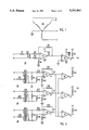
- FIG. 1 is a schematic diagram showing the source of a three phase alternating signal in a wye connection including a neutral.
- FIG. 2 (a and b) are circuit diagrams of the control circuit portion of the apparatus of the present invention showing the generation of the control signals used in the rectification of the three-phase AC signal.
- FIG. 3 is another diagram of a portion of the control circuit of the apparatus of the present invention using the output signals of the circuits shown in FIG. 2 to generate the first and second control signals.
- FIG. 4 is the rectification circuit portion of the apparatus of the present invention showing the three-phase AC signal and neutral, and the control signals used to generate the full wave rectified signal.
- FIG. 5 (a-m) are wave forms developed or used in various parts of the apparatus of the present invention.
- the three signals, A, B and C and the neutral N provide an alternating current signal and are used by the apparatus of the present invention to provide a full wave rectification.
- Each of the three phases A, B, C is an alternating current signal with respect to the neutral and is substantially 120° out of phase with another.
- a typical wave form is shown in FIG. 5(a).
- the voltage phase signals A, B and C are used to generate the control signals used in the apparatus of the present invention.
- a first control circuit 20 which receives one of the voltage phase signal.
- the voltage phase signal A has been chosen.
- the signal A and the neutral N are supplied to the circuit 20 comprising of a resistor R 1 , diode CR 1 and resistor R 2 connected in series. Since there is only onediode, the signal is rectified in a half cycle.
- U1 is an operational amplifier.
- U5 is a voltage comparator and serves to buffer the output of the half wave rectified signal.
- the output of the first control circuit 20at the node S will have a wave form shown in FIG. 5(c). As can be seen fromFIG.
- the signal S is a digital signal that is substantially zero during the positive phase of the A cycle and has a positive voltage duringthe negative half cycle of the A phase.
- the S signal is switched in phase with the A phase of the three-phase signal.
- the amplitude of the signal S is determined by the voltage reference connected to U5 and resistor R7. In the preferred embodiment, this voltage is +12 volts. Twelve volts is preferred as this is the voltage used in most CMOS digitalcircuits and analog circuits, U1 and U5.
- FIG. 2(b) is a second control circuit 22 which receives the reduced voltagephase signals A, B and C and the neutral N.
- the second control circuit 22 comprises three substantially identical portions 24, 26 and 28.
- the first portion 24 receives one of the voltage phase signal, such as A.
- the secondportion 26 receives another of the voltage phase signal B with a third portion 28 receiving the remaining voltage phase signal C.
- Each of the three portions 24, 26 and 28 also receives the neutral N and fully rectifies the voltage phase signal with respect to N through a bridge fullwave rectifier.
- the bridge is the diodes CR2, CR3, CR4 and CR5.
- the diodes are CR6, CR7, CR8 and CR9.
- the diodes are CR10, CR11, CR12 and CR13.
- the output of each of the portions 24, 26 and 28 at the nodes 30, 32 and 34 are the full waverectified signals A', B' and C' shown in FIG. 5(b).
- the output of the first portion 24, A' at the node 30 is supplied to a first comparator U6.
- the output of the second portion 26, B', at the output node 32 is also supplied to the first comparator U6 as the other input thereof.
- the outputs from the nodes 32 and 34 are supplied to the comparator U7.
- the output from the nodes 30 and 34 are supplied to the third comparator U8.
- the first comparator U6 compares the absolute magnitude of the fully-rectified A' signal to the fully rectified B' signal.
- the result is the control signal P.
- the control signal P whose wave form is shown in FIG. 5(d)
- the output of the second comparator U7 is the control signal Q whose wave form is shown in FIG. 5(e).
- the second comparator U7 compares the absolutemagnitude of the signal B' to the signal C'.
- the output of the third comparator U8 is the control signal R.
- the third comparator U8 compares the absolute magnitude of the signal C' to the absolute magnitudeof the signal A'.
- the wave forms for the control signals R is shown in FIG.5(f).
- the control signals S, P, Q and R are supplied to a logic circuit 40 shown in FIG. 3.
- the S signal is inverted by invertor U9 and is supplied to a NAND gate U13.
- the other inputs to the NAND gate U13 are the control signals P and R.
- the control signals S, P and Q are supplied asinputs to the NAND gate U14.
- the inputs to the NAND gate U15 are S, Q, and R.
- the output of the NAND gates U13, U14 and U15 has a wave formas shown in FIG. 5(g-i) respectively. These outputs are then supplied to aninverted input or gate U16.
- the output wave form of the gate U16 is shown in FIG. 5(j).
- the output of the gate U16 is inverted twice and becomes thecontrol signal CONT'L A.
- the output of the U16 is inverted three times and becomes the CONT'L B signal.
- the function of the capacitors C 1 and C 2 will be discussed hereinafter.
- the wave forms are shown in FIG. 5(k) and (l ), respectively.
- U20 and U21 are inverting buffers (drivers) which are used to drive the opto-isolators in FIG. 4.
- CONT'L A switches substantially every 60°.
- the switching is in phase with the commencement of a cycle of the A phase (this is because the voltage phase signal A was used to generate the S signal).
- the CONT'L A signal thus, is an oscillating signal that oscillates every 60° between 0 volts and +V voltage.
- the signal CONT'L B is 60° out of phase with the signal CONT'L A and oscillates between +V and 0 volts.
- FIG. 4 there is shown a schematic drawing of the rectificationcircuit 50 portion of the apparatus of the present invention.
- Each of the three-phase signals A, B, and C is supplied through a diode CR14, CR16 andCR18 respectively in a forward conduction manner and are connected to a common first node 52. From the first node 52, the signal travels through afuse F and through SCR switch SCR1. The signal path then passes through TM1which is a NTC thermistor which provides a "soft-start" to prevent sudden surges in current. The signal path is then supplied to the node V + and through a capacitor C. The capacitor C is used to eliminate the "ripples" in a full wave rectifier. The return path is from the node V - through an SCR switch SCR4 to the neutral line N.
- the negative phase of the cycle of the input phase signals A, B and C are supplied to the diodes CR15, CR17 and CR19, which are connected in opposite polarity to the diodes CR14, CR16, and CR18.
- the phase signals A, B and C are supplied to the second node 54.
- the signal path goes through a fuse F 2 and through the SCR switch SCR3.
- the signal passes through V - through the capacitor C and to the node V + .
- the signal passes through the SCR switch SCR2 and back to the neutral N.
- Each of the SCR switches SCR1, SCR2, SCR3, and SCR4 is regulated by an opto-isolated driver OP1, OP2, OP3 and OP4 respectively.
- the opto-isolateddrivers OP1 and OP4 are switched in tandem and are connected to the controlsignal CONT'L B.
- the opto-isolated drivers OP2 and OP3 are connected together and are switched in tandem and are connected to the signal CONT'LA.
- CONT'L A In the operation of the rectification circuit 50, between the cycle 0 and ⁇ /3, CONT'L A is low and CONT'L B is high. With CONT'L A low (i.e., at ground), opto-isolated drivers OP2 and OP3 would conduct causing SCR switches SCR2 and SCR3 to turn on. At the same time, CONT'L B would be high (i.e., at +V), causing opto-isolated drivers OP1 and OP4 to remain off. Thus, SCR switches SCR1 and SCR4 would be off.
- CONT'L A would be high and CONT'L B would be low. This would cause SCR switches SCR2 and SCR3 to be off and SCR switches SCR1 and SCR4 to be on. With the SCR switches SCR1 and SCR4 on, the signal path would be from the first node 52 through TM1 through the capacitor C through switch SCR4 to the neutral N. In this phase, the peak portion of the positive cycle of the A phase would be rectified.
- the apparatus 10 of the present invention may be practiced with circuit elements having the following values:
- the rectifying circuit of the present invention can provide full wave rectification from a three-phase signal to a neutral having highinput voltage on the order of 380 volts or 415 volts, without the need for a transformer.
Landscapes
- Engineering & Computer Science (AREA)
- Power Engineering (AREA)
- Rectifiers (AREA)
- Power Conversion In General (AREA)
Abstract
A full wave rectification circuit for use with a three-phase input signal connected in a wye configuration for rectifying a line to neutral high input voltage is disclosed. The rectification circuit has two portions. A first portion generates a control signal which oscillates every 60° and is switched in phase with one of the input signals. A second control signal, also oscillating in 60°, but completely out of phase with respect to the first oscillating signal is also generated. The two oscillating signals are used in a SCR switch configuration to switch the rectification circuit every 60° thereby rectifying the peak voltage portion of each phase.
Description
The present invention relates to a method and an apparatus for converting AC signal to a DC signal for a three-phase signal operating in a wye configuration. More particularly, the present invention can be used to convert the high voltages of a three-phase signal, such as 380 V(RMS) typically found in the European countries, without the need for a transformer.
The rectification of a multi-phase alternating current signal into a DC current signal is well known in the art. In U.S. Pat. No. 3,284,690, there is disclosed a half cycle rectifying apparatus for rectifying a multi-phase signal. Thus, the SCRS 20 and 22 (in FIG. 1 thereof) and SCRS 52, 54 and 56 (in FIG. 2 thereof) permit half cycle rectification.
In U.S. Pat. No. 3,434,032, there is disclosed a full wave rectifying apparatus for rectifying a multi-phase signal alternating between peak-to-peak. However, the neutral signal is not used in the rectification process. Thus, the apparatus rectifies a multi-phase signal connected in a delta configuration.
In U.S. Pat. No. 4,667,282, a three-phase full wave rectifier is disclosed in FIG. 1 thereof. As disclosed in that reference (see for example, Col. 4, lines 13-26), the apparatus operates as a full wave rectifier for a low input voltage and a half wave rectifier when the input voltage is high.
Heretofore, because of the different voltage standards in different parts of the world, a manufacturer of electrical equipment that requires DC power has attempted to manufacture a universal (adaptable in many countries) power rectifier by providing for a transformer. Thus, in the countries where the voltage of the alternating current signal is high, the transformer would lower the signal to an acceptable low value where a conventional full wave rectifier can be used thereon.
Thus, it is desired as one of the objects of the present invention, to provide a universal (adaptable in many countries, especially those countries employing high voltage alternating current signal) full wave power rectifier without the need for a transformer.
Other references which may be of relevant to this application include U.S. Pat. No. 4,184,075; 4,433,368; 4,495,557; 4,654,538; and 4,665,323.
In the present invention, a full wave rectifier for use with a multi-phase signal with each phase being an alternating current signal with respect to a neutral comprises means for receiving the neutral and each of the multi-phase signals. The full wave rectifier circuit also comprises a control circuit that generates a first control signal and a second control signal. The first control signal oscillates between a first voltage and a second voltage. The second control signal also oscillates between the first voltage and the second voltage, but is out of phase with respect to the first control signal. The rectification of each phase of the multi-phase signal is based upon the first control signal and the second control signal.
FIG. 1 is a schematic diagram showing the source of a three phase alternating signal in a wye connection including a neutral.
FIG. 2 (a and b) are circuit diagrams of the control circuit portion of the apparatus of the present invention showing the generation of the control signals used in the rectification of the three-phase AC signal.
FIG. 3 is another diagram of a portion of the control circuit of the apparatus of the present invention using the output signals of the circuits shown in FIG. 2 to generate the first and second control signals.
FIG. 4 is the rectification circuit portion of the apparatus of the present invention showing the three-phase AC signal and neutral, and the control signals used to generate the full wave rectified signal.
FIG. 5 (a-m) are wave forms developed or used in various parts of the apparatus of the present invention.
Referring to FIG. 1, there is shown a source 10 for providing a three-phasesignal (A, B, C) which is wye connected and includes a neutral, designated N. The three signals, A, B and C and the neutral N provide an alternating current signal and are used by the apparatus of the present invention to provide a full wave rectification. Each of the three phases A, B, C is an alternating current signal with respect to the neutral and is substantially 120° out of phase with another. A typical wave form is shown in FIG. 5(a).
The voltage phase signals A, B and C are used to generate the control signals used in the apparatus of the present invention.
Referring to FIG. 2(a), there is shown a first control circuit 20 which receives one of the voltage phase signal. For convenience, the voltage phase signal A has been chosen. The signal A and the neutral N are supplied to the circuit 20 comprising of a resistor R1, diode CR1 and resistor R2 connected in series. Since there is only onediode, the signal is rectified in a half cycle. U1 is an operational amplifier. U5 is a voltage comparator and serves to buffer the output of the half wave rectified signal. The output of the first control circuit 20at the node S will have a wave form shown in FIG. 5(c). As can be seen fromFIG. 5(c), the signal S is a digital signal that is substantially zero during the positive phase of the A cycle and has a positive voltage duringthe negative half cycle of the A phase. Thus, the S signal is switched in phase with the A phase of the three-phase signal. The amplitude of the signal S is determined by the voltage reference connected to U5 and resistor R7. In the preferred embodiment, this voltage is +12 volts. Twelve volts is preferred as this is the voltage used in most CMOS digitalcircuits and analog circuits, U1 and U5.
FIG. 2(b) is a second control circuit 22 which receives the reduced voltagephase signals A, B and C and the neutral N. The second control circuit 22 comprises three substantially identical portions 24, 26 and 28. The first portion 24 receives one of the voltage phase signal, such as A. The secondportion 26 receives another of the voltage phase signal B with a third portion 28 receiving the remaining voltage phase signal C. Each of the three portions 24, 26 and 28 also receives the neutral N and fully rectifies the voltage phase signal with respect to N through a bridge fullwave rectifier.
For the portion 24, the bridge is the diodes CR2, CR3, CR4 and CR5. For thesecond portion 26, the diodes are CR6, CR7, CR8 and CR9. For the third portion 28, the diodes are CR10, CR11, CR12 and CR13. The output of each of the portions 24, 26 and 28 at the nodes 30, 32 and 34 are the full waverectified signals A', B' and C' shown in FIG. 5(b).
The output of the first portion 24, A' at the node 30 is supplied to a first comparator U6. The output of the second portion 26, B', at the output node 32 is also supplied to the first comparator U6 as the other input thereof. Similarly, the outputs from the nodes 32 and 34 are supplied to the comparator U7. The output from the nodes 30 and 34 are supplied to the third comparator U8.
The first comparator U6 compares the absolute magnitude of the fully-rectified A' signal to the fully rectified B' signal. The result is the control signal P. The control signal P, whose wave form is shown in FIG. 5(d), is substantially zero where the absolute magnitude of the B' signal exceeds the A' signal and substantially has the voltage +V where the absolute magnitude of the A' signal exceeds the B' signal. Similarly, the output of the second comparator U7 is the control signal Q whose wave form is shown in FIG. 5(e). The second comparator U7 compares the absolutemagnitude of the signal B' to the signal C'. Finally, the output of the third comparator U8 is the control signal R. The third comparator U8 compares the absolute magnitude of the signal C' to the absolute magnitudeof the signal A'. The wave forms for the control signals R is shown in FIG.5(f).
The control signals S, P, Q and R are supplied to a logic circuit 40 shown in FIG. 3. The S signal is inverted by invertor U9 and is supplied to a NAND gate U13. The other inputs to the NAND gate U13 are the control signals P and R. Similarly, the control signals S, P and Q are supplied asinputs to the NAND gate U14. Finally, the inputs to the NAND gate U15 are S, Q, and R. The output of the NAND gates U13, U14 and U15 has a wave formas shown in FIG. 5(g-i) respectively. These outputs are then supplied to aninverted input or gate U16. The output wave form of the gate U16 is shown in FIG. 5(j). The output of the gate U16 is inverted twice and becomes thecontrol signal CONT'L A. The output of the U16 is inverted three times and becomes the CONT'L B signal. The function of the capacitors C1 and C2 will be discussed hereinafter. The wave forms are shown in FIG. 5(k) and (l ), respectively. U20 and U21 are inverting buffers (drivers) which are used to drive the opto-isolators in FIG. 4.
As can be seen from FIG. 5 waveform, CONT'L A switches substantially every 60°. The switching is in phase with the commencement of a cycle of the A phase (this is because the voltage phase signal A was used to generate the S signal). The CONT'L A signal, thus, is an oscillating signal that oscillates every 60° between 0 volts and +V voltage. The signal CONT'L B is 60° out of phase with the signal CONT'L A and oscillates between +V and 0 volts. When CONT'L A is at 0 volts CONT'L B is at +V whereas when CONT'L A is at +V volts CONT'L B is at 0 volts.
Referring to FIG. 4 there is shown a schematic drawing of the rectificationcircuit 50 portion of the apparatus of the present invention. Each of the three-phase signals A, B, and C is supplied through a diode CR14, CR16 andCR18 respectively in a forward conduction manner and are connected to a common first node 52. From the first node 52, the signal travels through afuse F and through SCR switch SCR1. The signal path then passes through TM1which is a NTC thermistor which provides a "soft-start" to prevent sudden surges in current. The signal path is then supplied to the node V+ and through a capacitor C. The capacitor C is used to eliminate the "ripples" in a full wave rectifier. The return path is from the node V- through an SCR switch SCR4 to the neutral line N.
The negative phase of the cycle of the input phase signals A, B and C are supplied to the diodes CR15, CR17 and CR19, which are connected in opposite polarity to the diodes CR14, CR16, and CR18. Through the negativephase, the phase signals A, B and C are supplied to the second node 54. From the second node 54, the signal path goes through a fuse F2 and through the SCR switch SCR3. From the SCR switch SCR3, the signal passes through V- through the capacitor C and to the node V+. From the node V+, the signal passes through the SCR switch SCR2 and back to the neutral N.
Each of the SCR switches SCR1, SCR2, SCR3, and SCR4 is regulated by an opto-isolated driver OP1, OP2, OP3 and OP4 respectively. The opto-isolateddrivers OP1 and OP4 are switched in tandem and are connected to the controlsignal CONT'L B. The opto-isolated drivers OP2 and OP3 are connected together and are switched in tandem and are connected to the signal CONT'LA.
In the operation of the rectification circuit 50, between the cycle 0 and π/3, CONT'L A is low and CONT'L B is high. With CONT'L A low (i.e., at ground), opto-isolated drivers OP2 and OP3 would conduct causing SCR switches SCR2 and SCR3 to turn on. At the same time, CONT'L B would be high (i.e., at +V), causing opto-isolated drivers OP1 and OP4 to remain off. Thus, SCR switches SCR1 and SCR4 would be off.
When SCR switches SCR2 and SCR3 are on, the signal path flows from second node 54 through second switch SCR3, through the capacitor C, through TM1, and through SCR switch SCR2, to neutral N. In this manner, the negative peak cycle portion of the B phase would be rectified.
During the next cycle of 60°, CONT'L A would be high and CONT'L B would be low. This would cause SCR switches SCR2 and SCR3 to be off and SCR switches SCR1 and SCR4 to be on. With the SCR switches SCR1 and SCR4 on, the signal path would be from the first node 52 through TM1 through the capacitor C through switch SCR4 to the neutral N. In this phase, the peak portion of the positive cycle of the A phase would be rectified.
Finally, in the third 60° phase, the switches SCR2 and SCR3 would beon and switches SCR1 and SCR4 would be off. This causes a conduction path from the second node 54 through switch SCR3 through the capacitor C through TM1 and through switch SCR2 to the neutral N. During this 60°, the peak negative cycle of the C phase would be rectified. Theresultant waveform is shown in FIG. 5(m) excluding the effect of the capacitor C. With the capacitor C, the waveform would be substantially constant at the V+.
In the preferred embodiment of the present invention, the apparatus 10 of the present invention may be practiced with circuit elements having the following values:
______________________________________
Resistor R1 =             15.6 kΩ
Resistor R2 =              1.0 kΩ
Resistor R3, R4, R5, R6 = 23.7 kΩ
Resistor R7 =              5.1 kΩ
Diodes CR1-CR13 =         IN4007
Resistors R8, R15, and R22 =
                          15.6 kΩ
Resistors R9, R16, and R23 =
                           1.0 kΩ
Resistors R10-R13, R17-R20, and R24-R27 =
                          23.7 kΩ
Resistors R14, R21, and R28 =
                           5.1 kΩ
Amplifiers U1, U2, U3, and U4 =
                          LM 324
Comparators U5, U6, U7, and U8 =
                          LM 339
Invertors U9, U10, U11, U12, U17, U18, U19 =
                          CD4049UB
NAND gates U13, U14, U15 and U16 =
                          CD4023B
Inverted Buffers U20 and U21 =
                          ULN 2004A
Diode Bridges CR14-CR19 = S7006-1
Opto-isolated drivers OP1, OP2, OP3 and OP4 =
                          MOC3001
Load resistors R31, R34, R37, and R40 =
                           1.0 kΩ
SCR switches SCR1-SCR4 =  S4060D
Resistors R29, R32, R35 and R38 =
                          47 Ω
Resistors R30, R33, R36 and R39 =
                          56 kΩ
______________________________________
Capacitors C1 and C2 are used to adjust switching off time of the SCR
 switches in case they are needed
There are many advantages to the method and apparatus of the present invention. The rectifying circuit of the present invention can provide full wave rectification from a three-phase signal to a neutral having highinput voltage on the order of 380 volts or 415 volts, without the need for a transformer.
Claims (9)
1. A full wave rectifier for use with a multi-phase signal each phase being an alternating current signal with respect to a neutral, said rectifier comprising:
means for receiving said neutral and said multi-phase signal and for generating a first control signal oscillating between a first voltage and a second voltage and a second control signal oscillating between said first voltage and said second voltage out of phase with respect to the first control signal, in response thereto; and
means for rectifying each phase of said multi-phase signal based upon said first and second control signals.
2. The rectifier of claim 1 wherein said multi-phase signal comprises three phases, each being substantially 120° out of phase with another.
3. The rectifier of claim 2 wherein said first control signal oscillates substantially every 60°.
4. A full wave rectifier for use with a three-phase (hereinafter referred to as: first phase, second phase and third phase) signal operating in a wye configuration, each of said three-phase signal is an A.C. signal with respect to a neutral, alternating in a full cycle, substantially one-hundred twenty degrees out of phase with another, said rectifier comprising:
means for generating a first control signal, said first control signal oscillating substantially every sixty degrees;
means for generating a second control signal, said second control signal, having the same polarity of oscillation as said first control signal, but out of phase with respect thereto; and
means for rectifying each of said three-phase signal based upon said first and second control signals.
5. The rectifier of claim 4 wherein said means for generating said first control signal further comprising:
means for generating a phase control signal based upon one of said three-phase signals;
means for comparing the absolute magnitude of said first phase signal to the absolute magnitude of said second phase signal to generate a first signal;
means for comparing the absolute magnitude of said second phase signal to the absolute magnitude of said third phase signal to generate a second signal;
means for comparing the absolute magnitude of said third phase signal to the absolute magnitude of said first phase signal to generate a third signal;
logic means for combining said first signal, said second signal, said third signal and said phase control signal to produce said first control signal.
6. The rectifier of claim 5 wherein said means for generating said second control signal further comprises:
invertor means for receiving said first control signal and for generating said second control signal in response thereto.
7. The rectifier of claim 4 wherein said means for rectifying comprises:
a first node;
a first set of diode means;
each of said three-phase signal is connected to said first node through a diode means of said first set for passing said three-phase signal in one polarity;
a second node;
a second set of diode means;
each of said three-phase signal is connected to said second node through a diode means of said second set for passing said three-phase signal in a polarity opposite said one polarity;
a first signal path from said first node to said neutral;
a second signal path from said second node to said neutral;
a first switch means positioned in said first signal path;
a second switch means positioned in said first signal path;
said first and second switch means switched in tandem and is responsive to said first control signal being in one polarity;
a third switch means positioned in said second signal path;
a fourth switch means positioned in said second signal path; and
a third and fourth switch means switched in tandem and is responsive to said second control signal being in said one polarity.
8. The rectifier of claim 7 wherein each of said first, second, third and fourth switch means is an SCR switch controlled by an opto-isolated driver.
9. A method of rectifying a three-phase signal operating in a wye configuration, each of said three-phase signal is an A.C. signal with respect to a common neutral alternating in a full cycle, substantially one hundred twenty degrees out of phase with another, said method comprising:
generating a first control signal, said first control signal oscillating substantially every sixty degrees, with the oscillation in phase with the commencement of a full cycle of one of the three-phase signal;
generating a second control signal, said second control signal oscillating out of phase with said first control signal;
rectifying said three-phase signal in response to said first and second control signals.
Priority Applications (6)
| Application Number | Priority Date | Filing Date | Title |
|---|---|---|---|
| US07/557,908 US5051883A (en) | 1990-07-25 | 1990-07-25 | Method and an apparatus for full wave rectification of a three-phase signal operating in a wye configuration |
| EP91912262A EP0540537B1 (en) | 1990-07-25 | 1991-06-21 | Method and apparatus for full wave rectification of a three-phase signal operating in a wye configuration |
| DE69112215T DE69112215T2 (en) | 1990-07-25 | 1991-06-21 | METHOD AND DEVICE FOR FULL-WAVE RECTIFICATION OF A THREE-PHASE SIGNAL IN A STAR CIRCUIT. |
| PCT/US1991/004420 WO1992002075A1 (en) | 1990-07-25 | 1991-06-21 | Method and apparatus for full wave rectification of a three-phase signal operating in a wye configuration |
| AT91912262T ATE126632T1 (en) | 1990-07-25 | 1991-06-21 | METHOD AND DEVICE FOR FULL WAVE RECTIFICATION OF A THREE-PHASE SIGNAL IN A STAR CONNECTION. |
| AU80587/91A AU8058791A (en) | 1990-07-25 | 1991-06-21 | Method and apparatus for full wave rectification of a three-phase signal operating in a wye configuration |
Applications Claiming Priority (1)
| Application Number | Priority Date | Filing Date | Title |
|---|---|---|---|
| US07/557,908 US5051883A (en) | 1990-07-25 | 1990-07-25 | Method and an apparatus for full wave rectification of a three-phase signal operating in a wye configuration |
Publications (1)
| Publication Number | Publication Date |
|---|---|
| US5051883A true US5051883A (en) | 1991-09-24 |
Family
ID=24227360
Family Applications (1)
| Application Number | Title | Priority Date | Filing Date |
|---|---|---|---|
| US07/557,908 Expired - Fee Related US5051883A (en) | 1990-07-25 | 1990-07-25 | Method and an apparatus for full wave rectification of a three-phase signal operating in a wye configuration |
Country Status (6)
| Country | Link |
|---|---|
| US (1) | US5051883A (en) |
| EP (1) | EP0540537B1 (en) |
| AT (1) | ATE126632T1 (en) |
| AU (1) | AU8058791A (en) |
| DE (1) | DE69112215T2 (en) |
| WO (1) | WO1992002075A1 (en) |
Cited By (4)
| Publication number | Priority date | Publication date | Assignee | Title |
|---|---|---|---|---|
| US5477128A (en) * | 1993-07-30 | 1995-12-19 | Technical Associates Co., Ltd. | Automatic charging apparatus |
| US6549438B2 (en) * | 2001-04-30 | 2003-04-15 | Precision Automation, Inc. | AC-to-DC converter circuit utilizing IGBT's for improved efficiency |
| US20130169040A1 (en) * | 2010-03-16 | 2013-07-04 | Sc2N | Switching device for the top-end of an automobile vehicle steering column |
| US12562652B2 (en) * | 2022-08-18 | 2026-02-24 | Delta Electronics, Inc. | Electronic transformer and three-phase four-wire power system thereof |
Families Citing this family (1)
| Publication number | Priority date | Publication date | Assignee | Title |
|---|---|---|---|---|
| US7521990B2 (en) * | 2006-10-12 | 2009-04-21 | Bybee Power, Llc | Noise reduction circuits |
Citations (4)
| Publication number | Priority date | Publication date | Assignee | Title |
|---|---|---|---|---|
| US4156896A (en) * | 1978-04-10 | 1979-05-29 | General Electric Company | Method of controlling a power conversion system |
| US4309749A (en) * | 1979-05-13 | 1982-01-05 | Siemens Aktiengesellschaft | Circuit having improved firing angle symmetry for ignition pulses in the control of a multipulse rectifier |
| US4672526A (en) * | 1984-07-27 | 1987-06-09 | Mitec, Moderne Industrietechnik Gmbh | Rectifying circuit arrangement for generating at least one controllable direct voltage from at least one alternating voltage |
| US4924371A (en) * | 1989-07-10 | 1990-05-08 | General Electric Company | Rectifier circuit provoding compression of the dynamic range of the output voltage |
Family Cites Families (10)
| Publication number | Priority date | Publication date | Assignee | Title |
|---|---|---|---|---|
| US3284690A (en) * | 1963-05-22 | 1966-11-08 | Fastener Corp | Controlled power supply circuit |
| DE1488033B1 (en) * | 1963-12-05 | 1969-09-25 | Siemens Ag | Arrangement for controlling the average direct current flowing through a consumer by means of thyristors |
| US3376494A (en) * | 1965-05-20 | 1968-04-02 | Power Conversion Inc | High frequency controlled rectifier circuit |
| US3434032A (en) * | 1967-06-20 | 1969-03-18 | Borg Warner | Rectifier system with integral cycle control |
| US4495557A (en) * | 1979-01-22 | 1985-01-22 | Contraves Goerz Corporation | Switching controller directly operable from AC |
| US4433368A (en) * | 1981-04-01 | 1984-02-21 | Samsung Electronics Co., Ltd. | Power supply circuit for a variable electrical source |
| DE3344105A1 (en) * | 1983-12-07 | 1985-06-27 | Deutsche Thomson-Brandt Gmbh, 7730 Villingen-Schwenningen | Network rectifier for two network voltages of different magnitude |
| US4665323A (en) * | 1984-10-25 | 1987-05-12 | Zenith Electronics Corporation | Electronically switchable power source |
| US4654538A (en) * | 1984-11-05 | 1987-03-31 | Burroughs Corporation | Dual input voltage power supply |
| US4667282A (en) * | 1985-12-16 | 1987-05-19 | General Electric Company | Multiphase rectifier circuit with dynamic AC input to DC output voltage range compression utilizing half and full wave rectification modes |
-
1990
- 1990-07-25 US US07/557,908 patent/US5051883A/en not_active Expired - Fee Related
-
1991
- 1991-06-21 AU AU80587/91A patent/AU8058791A/en not_active Abandoned
- 1991-06-21 WO PCT/US1991/004420 patent/WO1992002075A1/en not_active Ceased
- 1991-06-21 DE DE69112215T patent/DE69112215T2/en not_active Expired - Fee Related
- 1991-06-21 EP EP91912262A patent/EP0540537B1/en not_active Expired - Lifetime
- 1991-06-21 AT AT91912262T patent/ATE126632T1/en not_active IP Right Cessation
Patent Citations (4)
| Publication number | Priority date | Publication date | Assignee | Title |
|---|---|---|---|---|
| US4156896A (en) * | 1978-04-10 | 1979-05-29 | General Electric Company | Method of controlling a power conversion system |
| US4309749A (en) * | 1979-05-13 | 1982-01-05 | Siemens Aktiengesellschaft | Circuit having improved firing angle symmetry for ignition pulses in the control of a multipulse rectifier |
| US4672526A (en) * | 1984-07-27 | 1987-06-09 | Mitec, Moderne Industrietechnik Gmbh | Rectifying circuit arrangement for generating at least one controllable direct voltage from at least one alternating voltage |
| US4924371A (en) * | 1989-07-10 | 1990-05-08 | General Electric Company | Rectifier circuit provoding compression of the dynamic range of the output voltage |
Cited By (5)
| Publication number | Priority date | Publication date | Assignee | Title |
|---|---|---|---|---|
| US5477128A (en) * | 1993-07-30 | 1995-12-19 | Technical Associates Co., Ltd. | Automatic charging apparatus |
| US6549438B2 (en) * | 2001-04-30 | 2003-04-15 | Precision Automation, Inc. | AC-to-DC converter circuit utilizing IGBT's for improved efficiency |
| US20130169040A1 (en) * | 2010-03-16 | 2013-07-04 | Sc2N | Switching device for the top-end of an automobile vehicle steering column |
| US9643547B2 (en) * | 2010-03-16 | 2017-05-09 | Sc2N | Switching device for the top-end of an automobile vehicle steering column |
| US12562652B2 (en) * | 2022-08-18 | 2026-02-24 | Delta Electronics, Inc. | Electronic transformer and three-phase four-wire power system thereof |
Also Published As
| Publication number | Publication date |
|---|---|
| WO1992002075A1 (en) | 1992-02-06 |
| ATE126632T1 (en) | 1995-09-15 |
| AU8058791A (en) | 1992-02-18 |
| DE69112215T2 (en) | 1996-04-04 |
| EP0540537A4 (en) | 1993-12-15 |
| EP0540537B1 (en) | 1995-08-16 |
| DE69112215D1 (en) | 1995-09-21 |
| EP0540537A1 (en) | 1993-05-12 |
Similar Documents
| Publication | Publication Date | Title |
|---|---|---|
| US5317498A (en) | Electrical power generation system | |
| CA2174684C (en) | Rectifier control system | |
| US4904919A (en) | Dual mode control of a PWM motor drive for current limiting | |
| JPH01303060A (en) | Parallel operation equipment for ac output converter | |
| Vincenti et al. | A three-phase regulated PWM rectifier with on-line feedforward input unbalance correction | |
| US4435632A (en) | Three phase square wave welding power supply | |
| KR930024269A (en) | Parallel operation control device of pulse width modulation (PWM) inverter | |
| US5051883A (en) | Method and an apparatus for full wave rectification of a three-phase signal operating in a wye configuration | |
| US4186435A (en) | Device for controlling a Graetz rectifier bridge | |
| US5301098A (en) | Feedforward inverter phase control | |
| US4841426A (en) | Method for controlling the semiconductor switches of a rectifier bridge connected to an a.c. mains supply, and a control unit designed for applying the method | |
| CA1050106A (en) | Circuit arrangement with a number of cycloconverters, particularly direct cycloconverters in y-connection | |
| US4156275A (en) | Power conversion unit | |
| JPS5826569A (en) | Method and device for controlling output current of frequency converter | |
| JPS6118439B2 (en) | ||
| JP2676937B2 (en) | Harmonic compensator | |
| Enjeti et al. | A new current control scheme for AC motor drives | |
| JPS6035890B2 (en) | circuit constant generator | |
| JPS6035892B2 (en) | power converter | |
| JPH0452719B2 (en) | ||
| JPS5819169A (en) | Controlling method for pwm control converter | |
| KR820002332B1 (en) | Apparatus of generating waveform for a pwm-driven motor | |
| US3636373A (en) | Limit defining firing wave generator | |
| NO156030B (en) | DEVICE FOR AA GENERATING APPROXIMATELY STAPHESE AC VOLTAGE AT THREE-PHASE OUTPUTS FROM A DIRECT CONVERTER. | |
| FI911379A0 (en) | FARING REQUIREMENTS FOR PULSATING PULSVAEXELRIKTARE. |
Legal Events
| Date | Code | Title | Description |
|---|---|---|---|
| CC | Certificate of correction | ||
| REMI | Maintenance fee reminder mailed | ||
| FPAY | Fee payment |
Year of fee payment: 4 |
|
| SULP | Surcharge for late payment | ||
| REMI | Maintenance fee reminder mailed | ||
| LAPS | Lapse for failure to pay maintenance fees | ||
| FP | Lapsed due to failure to pay maintenance fee |
Effective date: 19990924 |
|
| STCH | Information on status: patent discontinuation |
Free format text: PATENT EXPIRED DUE TO NONPAYMENT OF MAINTENANCE FEES UNDER 37 CFR 1.362 |