US5017807A - Output buffer having capacitive drive shunt for reduced noise - Google Patents
Output buffer having capacitive drive shunt for reduced noise Download PDFInfo
- Publication number
- US5017807A US5017807A US07/549,519 US54951990A US5017807A US 5017807 A US5017807 A US 5017807A US 54951990 A US54951990 A US 54951990A US 5017807 A US5017807 A US 5017807A
- Authority
- US
- United States
- Prior art keywords
- transistor
- pull
- buffer
- shunt
- integrated circuit
- Prior art date
- Legal status (The legal status is an assumption and is not a legal conclusion. Google has not performed a legal analysis and makes no representation as to the accuracy of the status listed.)
- Expired - Lifetime
Links
Images


Classifications
-
- H—ELECTRICITY
- H03—ELECTRONIC CIRCUITRY
- H03K—PULSE TECHNIQUE
- H03K19/00—Logic circuits, i.e. having at least two inputs acting on one output; Inverting circuits
- H03K19/003—Modifications for increasing the reliability for protection
- H03K19/00369—Modifications for compensating variations of temperature, supply voltage or other physical parameters
- H03K19/00384—Modifications for compensating variations of temperature, supply voltage or other physical parameters in field effect transistor circuits
-
- H—ELECTRICITY
- H03—ELECTRONIC CIRCUITRY
- H03K—PULSE TECHNIQUE
- H03K19/00—Logic circuits, i.e. having at least two inputs acting on one output; Inverting circuits
- H03K19/003—Modifications for increasing the reliability for protection
- H03K19/00346—Modifications for eliminating interference or parasitic voltages or currents
- H03K19/00361—Modifications for eliminating interference or parasitic voltages or currents in field effect transistor circuits
Definitions
- the present invention relates to an integrated circuit buffer having a capacitive shunt circuit that reduces the noise generated by the buffer.
- Integrated circuit output buffers are used to drive a load connected to an external conductor.
- This load typically includes a relatively large capacitance, and in some cases a significant resistive load also.
- the output transistors are usually sized to be sufficiently large so as to drive the load at the maximum desired switching speed under worst case conditions.
- Such worst case conditions typically include a "slow" process, which is a deviation form the nominal fabrication process that yields an integrated circuit that operates at the low end of the acceptable speed range.
- operation at high temperature, and low power supply voltage are also worst case conditions for most designs.
- compensating for these worst case conditions in the design of the buffer may result in unacceptably high switching noise.
- Such noise may be due to capacitive or inductive coupling from the buffer circuitry to other circuitry on the integrated circuit, or onto external conductors connected thereto. It may also be due to power supply ground bounce due to the current flow as the buffer switches.
- One technique is to control the drive signal to the buffer, so as to reduce the drive level as processing variations, temperature changes, or power supply voltage variations tend to increase the switching speed.
- the buffer may still be designed to operate properly under worst case conditions. Then, under best case conditions, the switching speed, as determined by the rise and fall time of the buffer output voltage, remains relatively constant. Hence, the noise generated by the buffer remains relatively constant.
- One such technique is described in U.S. Pat. No. 4,823,029 co-assigned with the present invention. However, in some cases other techniques are desirable to control buffer switching noise.
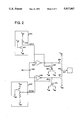
- FIG. 2 shows a second exemplary embodiment of the invention suitable for use as a CMOS output buffer.
- FIG. 3 shows a third exemplary embodiment of the invention suitable for use as a CMOS output buffer.
- the following detailed description relates to an integrated circuit having a buffer with a capacitive shunt circuit for controlling the drive signal to the buffer output stage, whereby buffer switching noise is reduced.
- the buffer output stage comprises a n-channel pull-up transistor 100 and a n-channel pull-down transistor 101 having their drains coupled to buffer output node 102.
- the buffer output node is connected to a bondpad 116 for connection to a package terminal, as by wire bonding or other techniques, whereby the buffer connects to an external load.
- the external load typically comprises a significant capacitive (AC) component and, in the case of a TTL load, an resistive (DC) component that requires pull-down current from the output buffer.
- the transistors 100 and 101 are sized accordingly, typically by assuming the worst-case conditions of the integrated circuit manufacturing process variations, operating temperature, and operating voltage.
- the control electrodes (i.e., gates) of transistors 100 and 101 receive complementary drive signals from current controlled inverters 103 and 104.
- the input signal to inverter 103 is made complementary with respect to the input signal to inverter 104 by inverter 105, which is connected to data input node 106.
- transistors 114 and 115 are controlled in a manner that tends to maintain the buffer switching speed more constant.
- the control of inverters 103 and 104 in this manner is further described in the above-noted U.S. Pat. No. 4,823,029. However, the control of the inverters 103 and 104 is optional insofar as the present invention is concerned.
- the resistor 112 is an off-chip resistor, to obtain a more constant value of resistance with respect to changes in the operating temperature of the integrated circuit. In one present design, a value of 900 ohms is used.
- the control voltage VCTL may be generated by other compensation circuitry than as shown in FIG. 1. For other examples, see the above-noted U.S. Pat. No. 4,823,029, with still others being possible.
- the shunt capacitors 108 and 110 are shown as MOS field effect devices having the gate electrode serve as one capacitor plate, the semiconductors substrate as the other capacitor plate, and the gate dielectric as the capacitor dielectric.
- a capacitance of about 2 picofarads is suitable for use with circuits implemented in 0.9 micrometer technology, and may be readily obtained.
- other capacitor types are possible, including, for example, deposited doped polysilicon layers separated by an oxide layer.
- the serial connection of the shunt transistor and shunt capacitor may be reversed; that is, the shunt capacitor may be connected to the gate of the buffer output transistor, and the shunt resistor may be connected between the shunt capacitor and ground.
- the shunt circuitry may be connected to another constant voltage source (e.g., V DD ), as determined by the characteristics of the devices use in its implementation.
- a second illustrative embodiment of the present invention is shown, wherein a CMOS buffer is shown for providing a full V SS to V DD output voltage swing (e.g., 0 to 5 volts).
- the output stage comprises a p-channel pull-up transistor 200, whereas the pull-down device is n-channel transistor 201.
- the shunt circuit for the p-channel output device 200 comprises transistor 207 and capacitor 208, which are shown as p-channel devices.
- the control voltage VCTLP is generated by compensation circuit 214 comprising n-channel transistor 215 and resistor 216. (Alternatively, the shunt transistor may be a n-channel device if desired, in which case the control voltage voltage is generated as in FIG.
- the foregoing implementations have shown the pull-up and pull-down transistors driven by separate driver stages (103, 104 in FIG. 1 and 203, 204 in FIG. 2). This allows the switching thresholds of the inverter stages to be separately chosen, typically to minimize the simultaneous "on" times of the pull-up and pull-down output transistors, in order to minimize power consumption. Furthermore, the separate drivers allows for readily implementing a tri-state design by additional logic circuitry (not shown) that can turn off both the pull-up and pull-down devices concurrently. The use of two separate shunt circuits for the two output transistors also allows the rise time (due to the pull-up transistor) to be controlled separately from the fall time (due to the pull-down transistor), if desired.
- the present technique may alternatively be used as shown in FIG. 3, wherein the output transistors 300 and 301 have their gates connected to a common input node 303.
- a single shunt circuit comprising shunt transistor 304 and shunt capacitor 305 provides the desired compensation of buffer speed by slowing down both the rise and fall times of the output voltage at node 302 according to the voltage VCTL, which may be generated as before.
Landscapes
- Physics & Mathematics (AREA)
- Engineering & Computer Science (AREA)
- Computer Hardware Design (AREA)
- Computing Systems (AREA)
- General Engineering & Computer Science (AREA)
- Mathematical Physics (AREA)
- Metal-Oxide And Bipolar Metal-Oxide Semiconductor Integrated Circuits (AREA)
- Electronic Switches (AREA)
- Logic Circuits (AREA)
Abstract
Description
Claims (8)
Priority Applications (2)
| Application Number | Priority Date | Filing Date | Title |
|---|---|---|---|
| US07/549,519 US5017807A (en) | 1990-07-05 | 1990-07-05 | Output buffer having capacitive drive shunt for reduced noise |
| JP3191250A JP2665079B2 (en) | 1990-07-05 | 1991-07-05 | Integrated circuit |
Applications Claiming Priority (1)
| Application Number | Priority Date | Filing Date | Title |
|---|---|---|---|
| US07/549,519 US5017807A (en) | 1990-07-05 | 1990-07-05 | Output buffer having capacitive drive shunt for reduced noise |
Publications (1)
| Publication Number | Publication Date |
|---|---|
| US5017807A true US5017807A (en) | 1991-05-21 |
Family
ID=24193345
Family Applications (1)
| Application Number | Title | Priority Date | Filing Date |
|---|---|---|---|
| US07/549,519 Expired - Lifetime US5017807A (en) | 1990-07-05 | 1990-07-05 | Output buffer having capacitive drive shunt for reduced noise |
Country Status (2)
| Country | Link |
|---|---|
| US (1) | US5017807A (en) |
| JP (1) | JP2665079B2 (en) |
Cited By (35)
| Publication number | Priority date | Publication date | Assignee | Title |
|---|---|---|---|---|
| US5103118A (en) * | 1990-11-19 | 1992-04-07 | National Semiconductor Corporation | High speed anti-undershoot and anti-overshoot circuit |
| US5136182A (en) * | 1990-08-31 | 1992-08-04 | Advanced Micro Devices, Inc. | Controlled voltage or current source, and logic gate with same |
| US5214320A (en) * | 1992-06-12 | 1993-05-25 | Smos Systems, Inc. | System and method for reducing ground bounce in integrated circuit output buffers |
| EP0557080A1 (en) * | 1992-02-18 | 1993-08-25 | Samsung Semiconductor, Inc. | Output buffer with controlled output level |
| US5248906A (en) * | 1992-06-12 | 1993-09-28 | Advanced Micro Devices, Inc. | High speed CMOS output buffer circuit minimizes output signal oscillation and steady state current |
| US5285116A (en) * | 1990-08-28 | 1994-02-08 | Mips Computer Systems, Inc. | Low-noise high-speed output buffer and method for controlling same |
| EP0587999A1 (en) * | 1992-09-16 | 1994-03-23 | International Business Machines Corporation | Transition-controlled off-chip driver |
| US5303191A (en) * | 1992-01-23 | 1994-04-12 | Motorola, Inc. | Memory with compensation for voltage, temperature, and processing variations |
| US5317206A (en) * | 1992-05-14 | 1994-05-31 | Mitsubishi Denki Kabushiki Kaisha | Buffer circuit using capacitors to control the slow rate of a driver transistor |
| EP0606727A1 (en) * | 1993-01-13 | 1994-07-20 | AT&T Corp. | Automatic control of buffer speed |
| US5341040A (en) * | 1991-08-29 | 1994-08-23 | National Semiconductor Corporation | High performance output buffer with reduced ground bounce |
| US5491430A (en) * | 1993-05-15 | 1996-02-13 | Kabushiki Kaisha Toshiba | Semiconductor integrated circuit device with data output circuit |
| US5498977A (en) * | 1995-03-03 | 1996-03-12 | Hewlett-Packard Company | Output driver having process, voltage and temperature compensation for delay and risetime |
| US5604448A (en) * | 1994-09-09 | 1997-02-18 | Hyundai Electronics Industries Co., Ltd. | Output buffer circuit having low noise characteristics |
| US5623216A (en) * | 1994-04-22 | 1997-04-22 | Sgs-Thomson Microelectronics S.R.L. | Output buffer current slew rate control integrated circuit |
| US5629634A (en) * | 1995-08-21 | 1997-05-13 | International Business Machines Corporation | Low-power, tristate, off-chip driver circuit |
| US5633600A (en) * | 1994-09-29 | 1997-05-27 | Nec Corporation | Output buffer circuit having a minimized output voltage propagation |
| US5657456A (en) * | 1993-06-18 | 1997-08-12 | Digital Equipment Corporation | Semiconductor process power supply voltage and temperature compensated integrated system bus driver rise and fall time |
| US5687330A (en) * | 1993-06-18 | 1997-11-11 | Digital Equipment Corporation | Semiconductor process, power supply and temperature compensated system bus integrated interface architecture with precision receiver |
| US5694065A (en) * | 1994-08-16 | 1997-12-02 | Burr-Brown Corporation | Switching control circuitry for low noise CMOS inverter |
| US5701090A (en) * | 1994-11-15 | 1997-12-23 | Mitsubishi Denki Kabushiki Kaisha | Data output circuit with reduced output noise |
| US5739714A (en) * | 1995-10-24 | 1998-04-14 | Lucent Technologies, Inc. | Apparatus for controlling ground bounce |
| US5923192A (en) * | 1997-02-26 | 1999-07-13 | Nippon Precision Circuits Inc. | CMOS circuit |
| US6285215B1 (en) * | 1999-09-02 | 2001-09-04 | Micron Technology, Inc. | Output driver having a programmable edge rate |
| WO2002003551A3 (en) * | 2000-06-30 | 2002-08-01 | Mosaid Technologies Inc | Digital delay element |
| US6463395B1 (en) * | 1999-12-10 | 2002-10-08 | Teradyne, Inc. | Shunt capacitance compensation structure and method for a signal channel |
| US6522208B1 (en) * | 1999-11-03 | 2003-02-18 | Bae Systems Information And Electronic Systems Integration, Inc. | Oscillator and method for generating a frequency within a stable frequency range |
| US6522180B1 (en) * | 2000-12-21 | 2003-02-18 | Intel Corporation | Bi-voltage levels switches |
| US20040095110A1 (en) * | 2002-11-14 | 2004-05-20 | Kent Kernahan | Power converter circuitry and method |
| US20040169973A1 (en) * | 2002-06-13 | 2004-09-02 | Kenneth Koch | Driver circuit connected to a switched capacitor and method of operating same |
| US20070268044A1 (en) * | 2005-03-22 | 2007-11-22 | Dong Pan | Output buffer and method having a supply voltage insensitive slew rate |
| US7605602B1 (en) | 2007-10-23 | 2009-10-20 | Lattice Semiconductor Corporation | Low-power output driver buffer circuit |
| US20100289562A1 (en) * | 2009-05-13 | 2010-11-18 | Fuji Electric Systems Co., Ltd. | Gate drive device |
| US20120313544A1 (en) * | 2009-11-06 | 2012-12-13 | Neofocal Systems, Inc. | Method And Apparatus For Efficiently Powering Digital Electronic Nodes On A Single Conductor Current Line |
| US20130049884A1 (en) * | 2011-08-22 | 2013-02-28 | Texas Instruments Incorporated | Methods and circuits for attenuating high-frequency noise |
Citations (7)
| Publication number | Priority date | Publication date | Assignee | Title |
|---|---|---|---|---|
| US4499387A (en) * | 1981-12-15 | 1985-02-12 | Tokyo Shibaura Denki Kabushiki Kaisha | Integrated circuit formed on a semiconductor substrate with a variable capacitor circuit |
| US4797579A (en) * | 1987-07-27 | 1989-01-10 | Raytheon Company | CMOS VLSI output driver with controlled rise and fall times |
| US4823029A (en) * | 1987-06-25 | 1989-04-18 | American Telephone And Telegraph Company At&T Bell Laboratories | Noise controlled output buffer |
| US4849661A (en) * | 1988-06-16 | 1989-07-18 | Intel Corporation | CMOS input buffer with switched capacitor reference voltage generator |
| US4859870A (en) * | 1987-10-14 | 1989-08-22 | Lsi Logic Incorporated | Two-mode driver circuit |
| US4894561A (en) * | 1987-12-18 | 1990-01-16 | Kabushiki Kaisha Toshiba | CMOS inverter having temperature and supply voltage variation compensation |
| US4947061A (en) * | 1989-02-13 | 1990-08-07 | At&T Bell Laboratories | CMOS to ECL output buffer circuit |
Family Cites Families (1)
| Publication number | Priority date | Publication date | Assignee | Title |
|---|---|---|---|---|
| JPH0770987B2 (en) * | 1990-01-31 | 1995-07-31 | 三洋電機株式会社 | Output buffer circuit |
-
1990
- 1990-07-05 US US07/549,519 patent/US5017807A/en not_active Expired - Lifetime
-
1991
- 1991-07-05 JP JP3191250A patent/JP2665079B2/en not_active Expired - Fee Related
Patent Citations (7)
| Publication number | Priority date | Publication date | Assignee | Title |
|---|---|---|---|---|
| US4499387A (en) * | 1981-12-15 | 1985-02-12 | Tokyo Shibaura Denki Kabushiki Kaisha | Integrated circuit formed on a semiconductor substrate with a variable capacitor circuit |
| US4823029A (en) * | 1987-06-25 | 1989-04-18 | American Telephone And Telegraph Company At&T Bell Laboratories | Noise controlled output buffer |
| US4797579A (en) * | 1987-07-27 | 1989-01-10 | Raytheon Company | CMOS VLSI output driver with controlled rise and fall times |
| US4859870A (en) * | 1987-10-14 | 1989-08-22 | Lsi Logic Incorporated | Two-mode driver circuit |
| US4894561A (en) * | 1987-12-18 | 1990-01-16 | Kabushiki Kaisha Toshiba | CMOS inverter having temperature and supply voltage variation compensation |
| US4849661A (en) * | 1988-06-16 | 1989-07-18 | Intel Corporation | CMOS input buffer with switched capacitor reference voltage generator |
| US4947061A (en) * | 1989-02-13 | 1990-08-07 | At&T Bell Laboratories | CMOS to ECL output buffer circuit |
Cited By (56)
| Publication number | Priority date | Publication date | Assignee | Title |
|---|---|---|---|---|
| US5285116A (en) * | 1990-08-28 | 1994-02-08 | Mips Computer Systems, Inc. | Low-noise high-speed output buffer and method for controlling same |
| US5136182A (en) * | 1990-08-31 | 1992-08-04 | Advanced Micro Devices, Inc. | Controlled voltage or current source, and logic gate with same |
| US5103118A (en) * | 1990-11-19 | 1992-04-07 | National Semiconductor Corporation | High speed anti-undershoot and anti-overshoot circuit |
| US5341040A (en) * | 1991-08-29 | 1994-08-23 | National Semiconductor Corporation | High performance output buffer with reduced ground bounce |
| US5303191A (en) * | 1992-01-23 | 1994-04-12 | Motorola, Inc. | Memory with compensation for voltage, temperature, and processing variations |
| EP0557080A1 (en) * | 1992-02-18 | 1993-08-25 | Samsung Semiconductor, Inc. | Output buffer with controlled output level |
| US5317206A (en) * | 1992-05-14 | 1994-05-31 | Mitsubishi Denki Kabushiki Kaisha | Buffer circuit using capacitors to control the slow rate of a driver transistor |
| US5214320A (en) * | 1992-06-12 | 1993-05-25 | Smos Systems, Inc. | System and method for reducing ground bounce in integrated circuit output buffers |
| US5248906A (en) * | 1992-06-12 | 1993-09-28 | Advanced Micro Devices, Inc. | High speed CMOS output buffer circuit minimizes output signal oscillation and steady state current |
| EP0587999A1 (en) * | 1992-09-16 | 1994-03-23 | International Business Machines Corporation | Transition-controlled off-chip driver |
| US5430387A (en) * | 1992-09-16 | 1995-07-04 | International Business Machines Corporation | Transition-controlled off-chip driver |
| US5334885A (en) * | 1993-01-13 | 1994-08-02 | At&T Bell Laboratories | Automatic control of buffer speed |
| EP0606727A1 (en) * | 1993-01-13 | 1994-07-20 | AT&T Corp. | Automatic control of buffer speed |
| JP3182035B2 (en) | 1993-01-13 | 2001-07-03 | エイ・ティ・アンド・ティ・コーポレーション | Automatic control of buffer speed |
| US5955891A (en) * | 1993-05-15 | 1999-09-21 | Kabushiki Kaisha Toshiba | Semiconductor integrated circuit device with output circuit |
| US5570038A (en) * | 1993-05-15 | 1996-10-29 | Kabushiki Kaisha Toshiba | Semiconductor integrated circuit device with data output circuit |
| US5491430A (en) * | 1993-05-15 | 1996-02-13 | Kabushiki Kaisha Toshiba | Semiconductor integrated circuit device with data output circuit |
| US5657456A (en) * | 1993-06-18 | 1997-08-12 | Digital Equipment Corporation | Semiconductor process power supply voltage and temperature compensated integrated system bus driver rise and fall time |
| US5687330A (en) * | 1993-06-18 | 1997-11-11 | Digital Equipment Corporation | Semiconductor process, power supply and temperature compensated system bus integrated interface architecture with precision receiver |
| US5623216A (en) * | 1994-04-22 | 1997-04-22 | Sgs-Thomson Microelectronics S.R.L. | Output buffer current slew rate control integrated circuit |
| US5694065A (en) * | 1994-08-16 | 1997-12-02 | Burr-Brown Corporation | Switching control circuitry for low noise CMOS inverter |
| US5604448A (en) * | 1994-09-09 | 1997-02-18 | Hyundai Electronics Industries Co., Ltd. | Output buffer circuit having low noise characteristics |
| US5633600A (en) * | 1994-09-29 | 1997-05-27 | Nec Corporation | Output buffer circuit having a minimized output voltage propagation |
| US5933048A (en) * | 1994-11-15 | 1999-08-03 | Mitsubishi Denki Kabushiki Kaisha | Data output circuit with reduced output noise |
| US20060028237A1 (en) * | 1994-11-15 | 2006-02-09 | Hideto Hidaka | Data output circuit with reduced output noise |
| US5701090A (en) * | 1994-11-15 | 1997-12-23 | Mitsubishi Denki Kabushiki Kaisha | Data output circuit with reduced output noise |
| USRE38213E1 (en) | 1994-11-15 | 2003-08-12 | Mitsubishi Denki Kabushiki Kaisha | Data output circuit with reduced output noise |
| US20040257112A1 (en) * | 1994-11-15 | 2004-12-23 | Renesas Technology Corp. | Data output circuit with reduced output noise |
| US6163180A (en) * | 1994-11-15 | 2000-12-19 | Mitsubishi Denki Kabushiki Kaisha | Data output circuit with reduced output noise |
| US6777986B2 (en) | 1994-11-15 | 2004-08-17 | Renesas Technology Corp. | Data output circuit with reduced output noise |
| US7250796B2 (en) | 1994-11-15 | 2007-07-31 | Renesas Technology Corp. | Semiconductor device including an output circuit having a reduced output noise |
| US20070132488A1 (en) * | 1994-11-15 | 2007-06-14 | Renesas Technology Corp. | Data output circuit with reduced output noise |
| US6445222B1 (en) | 1994-11-15 | 2002-09-03 | Mitsubishi Denki Kabushiki Kaisha | Data output circuit with reduced output noise |
| US6975147B2 (en) | 1994-11-15 | 2005-12-13 | Renesas Technology Corp. | Data output circuit with reduced output noise |
| US5498977A (en) * | 1995-03-03 | 1996-03-12 | Hewlett-Packard Company | Output driver having process, voltage and temperature compensation for delay and risetime |
| US5629634A (en) * | 1995-08-21 | 1997-05-13 | International Business Machines Corporation | Low-power, tristate, off-chip driver circuit |
| US5739714A (en) * | 1995-10-24 | 1998-04-14 | Lucent Technologies, Inc. | Apparatus for controlling ground bounce |
| US5923192A (en) * | 1997-02-26 | 1999-07-13 | Nippon Precision Circuits Inc. | CMOS circuit |
| US6285215B1 (en) * | 1999-09-02 | 2001-09-04 | Micron Technology, Inc. | Output driver having a programmable edge rate |
| US6522208B1 (en) * | 1999-11-03 | 2003-02-18 | Bae Systems Information And Electronic Systems Integration, Inc. | Oscillator and method for generating a frequency within a stable frequency range |
| US6463395B1 (en) * | 1999-12-10 | 2002-10-08 | Teradyne, Inc. | Shunt capacitance compensation structure and method for a signal channel |
| WO2002003551A3 (en) * | 2000-06-30 | 2002-08-01 | Mosaid Technologies Inc | Digital delay element |
| US6522180B1 (en) * | 2000-12-21 | 2003-02-18 | Intel Corporation | Bi-voltage levels switches |
| US20040169973A1 (en) * | 2002-06-13 | 2004-09-02 | Kenneth Koch | Driver circuit connected to a switched capacitor and method of operating same |
| US20040095110A1 (en) * | 2002-11-14 | 2004-05-20 | Kent Kernahan | Power converter circuitry and method |
| US6897683B2 (en) * | 2002-11-14 | 2005-05-24 | Fyre Storm, Inc. | Driver including first and second buffers for driving an external coil or first and second transistors |
| US20070268044A1 (en) * | 2005-03-22 | 2007-11-22 | Dong Pan | Output buffer and method having a supply voltage insensitive slew rate |
| US7528624B2 (en) * | 2005-03-22 | 2009-05-05 | Micron Technology, Inc. | Output buffer and method having a supply voltage insensitive slew rate |
| US20090201046A1 (en) * | 2005-03-22 | 2009-08-13 | Dong Pan | Output buffer and method having a supply voltage insensitive slew rate |
| US7795903B2 (en) | 2005-03-22 | 2010-09-14 | Micron Technology, Inc. | Output buffer and method having a supply voltage insensitive slew rate |
| US7605602B1 (en) | 2007-10-23 | 2009-10-20 | Lattice Semiconductor Corporation | Low-power output driver buffer circuit |
| US20100289562A1 (en) * | 2009-05-13 | 2010-11-18 | Fuji Electric Systems Co., Ltd. | Gate drive device |
| US8217704B2 (en) * | 2009-05-13 | 2012-07-10 | Fuji Electric Co., Ltd. | Gate drive device |
| US20120313544A1 (en) * | 2009-11-06 | 2012-12-13 | Neofocal Systems, Inc. | Method And Apparatus For Efficiently Powering Digital Electronic Nodes On A Single Conductor Current Line |
| US8456098B2 (en) * | 2009-11-06 | 2013-06-04 | Memoir Systems, Inc. | Method and apparatus for efficiently powering digital electronic nodes on a single conductor current line |
| US20130049884A1 (en) * | 2011-08-22 | 2013-02-28 | Texas Instruments Incorporated | Methods and circuits for attenuating high-frequency noise |
Also Published As
| Publication number | Publication date |
|---|---|
| JPH04233820A (en) | 1992-08-21 |
| JP2665079B2 (en) | 1997-10-22 |
Similar Documents
| Publication | Publication Date | Title |
|---|---|---|
| US5017807A (en) | Output buffer having capacitive drive shunt for reduced noise | |
| US5568062A (en) | Low noise tri-state output buffer | |
| EP0493873B1 (en) | CMOS output buffer circuit with ground bounce reduction | |
| US4779013A (en) | Slew-rate limited output driver having reduced switching noise | |
| US6593795B2 (en) | Level adjustment circuit and data output circuit thereof | |
| US4877980A (en) | Time variant drive circuit for high speed bus driver to limit oscillations or ringing on a bus | |
| US5214320A (en) | System and method for reducing ground bounce in integrated circuit output buffers | |
| EP0329285B1 (en) | Output buffer | |
| US5367210A (en) | Output buffer with reduced noise | |
| JPS60134544A (en) | Bus transceiver | |
| US5097148A (en) | Integrated circuit buffer with improved drive capability | |
| EP0346876B1 (en) | Semiconductor integrated circuit having a CMOS inverter | |
| US4823029A (en) | Noise controlled output buffer | |
| US5408191A (en) | Input buffer having a compensation circuit for stabilizing the output thereof | |
| US4845388A (en) | TTL-CMOS input buffer | |
| US6621329B2 (en) | Semiconductor device | |
| US5614842A (en) | Semiconductor integrated circuit with buffer circuit and manufacturing method thereof | |
| EP0347083B1 (en) | TTL output driver gate configuration | |
| US5227673A (en) | Differential output buffer with feedback | |
| US5343099A (en) | Output device capable of high speed operation and operating method thereof | |
| EP1341307B1 (en) | Logic circuit with compensation for the effects of process, voltage, and temperature variations | |
| US6175598B1 (en) | Output noise control scheme for multiple I/O's | |
| JP3175989B2 (en) | Output buffer circuit | |
| US20040119510A1 (en) | Bus driver | |
| US6288582B1 (en) | Output circuit for semiconductor integrated circuit |
Legal Events
| Date | Code | Title | Description |
|---|---|---|---|
| AS | Assignment |
Owner name: AMERICAN TELEPHONE AND TELEGRAPH COMPANY, A CORP. Free format text: ASSIGNMENT OF ASSIGNORS INTEREST.;ASSIGNORS:KRIZ, JOHN C.;TSAY, MEAN-SEA;REEL/FRAME:005376/0873;SIGNING DATES FROM 19900628 TO 19900705 |
|
| STCF | Information on status: patent grant |
Free format text: PATENTED CASE |
|
| FEPP | Fee payment procedure |
Free format text: PAYOR NUMBER ASSIGNED (ORIGINAL EVENT CODE: ASPN); ENTITY STATUS OF PATENT OWNER: LARGE ENTITY |
|
| FPAY | Fee payment |
Year of fee payment: 4 |
|
| FEPP | Fee payment procedure |
Free format text: PAYER NUMBER DE-ASSIGNED (ORIGINAL EVENT CODE: RMPN); ENTITY STATUS OF PATENT OWNER: LARGE ENTITY Free format text: PAYOR NUMBER ASSIGNED (ORIGINAL EVENT CODE: ASPN); ENTITY STATUS OF PATENT OWNER: LARGE ENTITY |
|
| FEPP | Fee payment procedure |
Free format text: PAYER NUMBER DE-ASSIGNED (ORIGINAL EVENT CODE: RMPN); ENTITY STATUS OF PATENT OWNER: LARGE ENTITY Free format text: PAYOR NUMBER ASSIGNED (ORIGINAL EVENT CODE: ASPN); ENTITY STATUS OF PATENT OWNER: LARGE ENTITY |
|
| FPAY | Fee payment |
Year of fee payment: 8 |
|
| FEPP | Fee payment procedure |
Free format text: PAYER NUMBER DE-ASSIGNED (ORIGINAL EVENT CODE: RMPN); ENTITY STATUS OF PATENT OWNER: LARGE ENTITY Free format text: PAYOR NUMBER ASSIGNED (ORIGINAL EVENT CODE: ASPN); ENTITY STATUS OF PATENT OWNER: LARGE ENTITY |
|
| FPAY | Fee payment |
Year of fee payment: 12 |