US5003169A - Photoelectric switch having changeable length - Google Patents
Photoelectric switch having changeable length Download PDFInfo
- Publication number
- US5003169A US5003169A US07/428,728 US42872889A US5003169A US 5003169 A US5003169 A US 5003169A US 42872889 A US42872889 A US 42872889A US 5003169 A US5003169 A US 5003169A
- Authority
- US
- United States
- Prior art keywords
- light
- unit
- relay unit
- elements
- housing
- Prior art date
- Legal status (The legal status is an assumption and is not a legal conclusion. Google has not performed a legal analysis and makes no representation as to the accuracy of the status listed.)
- Expired - Lifetime
Links
- 238000001514 detection method Methods 0.000 claims description 22
- 230000003287 optical effect Effects 0.000 description 8
- 239000000758 substrate Substances 0.000 description 8
- 238000010586 diagram Methods 0.000 description 6
- 238000000034 method Methods 0.000 description 5
- 238000005260 corrosion Methods 0.000 description 3
- 230000007797 corrosion Effects 0.000 description 3
- 238000012986 modification Methods 0.000 description 3
- 230000004048 modification Effects 0.000 description 3
- 230000001681 protective effect Effects 0.000 description 3
- 239000012780 transparent material Substances 0.000 description 3
- 230000006641 stabilisation Effects 0.000 description 2
- 238000011105 stabilization Methods 0.000 description 2
- 230000002411 adverse Effects 0.000 description 1
- 230000003247 decreasing effect Effects 0.000 description 1
- 230000003111 delayed effect Effects 0.000 description 1
- 238000001125 extrusion Methods 0.000 description 1
- 238000012856 packing Methods 0.000 description 1
Images


Classifications
-
- H—ELECTRICITY
- H01—ELECTRIC ELEMENTS
- H01H—ELECTRIC SWITCHES; RELAYS; SELECTORS; EMERGENCY PROTECTIVE DEVICES
- H01H35/00—Switches operated by change of a physical condition
-
- G—PHYSICS
- G01—MEASURING; TESTING
- G01V—GEOPHYSICS; GRAVITATIONAL MEASUREMENTS; DETECTING MASSES OR OBJECTS; TAGS
- G01V8/00—Prospecting or detecting by optical means
- G01V8/10—Detecting, e.g. by using light barriers
- G01V8/20—Detecting, e.g. by using light barriers using multiple transmitters or receivers
Definitions
- the present invention relates to a photoelectric switch in which a light-emitting section composed of a plurality of light-emitting elements is confronted with a light-detecting section composed of a plurality of light-detecting elements, thus forming a multi-optical-path. More particularly, the invention relates to a photoelectric switch in which the degree of freedom in the arrangement of optical paths is improved.
- a photoelectric switch as shown in FIG. 35 has generally been employed.
- the switch has a light-detecting section 1 in which a plurality of light-detecting elements 2 are arranged in a line, and a light-emitting section 3 in which a plurality of light-emitting elements 4 are arranged in such a manner as to confront with respective ones of the light-detecting elements 2. Accordingly, a plurality of optical paths 5 are formed between the light-detecting elements 2 and the light-emitting elements 4.
- a detection plane 6 (indicated by a two-dot chain line) and crosses at least one optical path 5
- a light beam from at least one light-emitting element 4 is not applied to the confronting light-detecting element 2, whereby the presence of the object can be detected.
- the light-emitting section 3 and the light-detecting 1 section are constant in length. Hence, in order to change the size of the detection plane 6 according to the object to be detected, a plurality of photoelectric switches different in length must be provided.
- an object for instance in the case of an object having a hole, sometimes it is necessary to provide a non-detection region in a part of the detection plane 6. In this case, it is necessary to additionally provide a photoelectric switch which has a non-detection part. Furthermore, in order to change the position of the non-detection region, it is necessary to provide a photoelectric switch which is different in the arrangement of light-emitting and light-detecting elements.
- an object of this invention is to provide a photoelectric switch which can handle a variety of objects different in size and configuration.
- a photoelectric switch comprising a light-emitting section having a plurality of aligned light-emitting elements, and a light-detecting section having a plurality of light-detecting elements aligned in such a manner as to confront with respective ones of the light-emitting elements, in which each of the light-emitting section and light-detecting section comprises: a base unit including a housing accommodating the elements and an electrical circuit, the housing having a step substantially at the middle portion thereof formed in such a manner that the housing is divided into a connected part, which extends from the step towards one of the ends of the housing, and a base part, which extends towards the other end, the connected part being thinner than the base part, the base unit having openings in the front surface thereof at equal intervals in which the elements are arranged; a relay unit including a housing into which the connected part of the base unit is inserted and which accommodates the elements and an electrical circuit, the housing of the relay unit having a step substantially
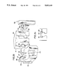
- FIG. 1 is a perspective view showing a first example of a photoelectric switch constructed according to this invention
- FIGS. 2 through 5 show a base unit in the photoelectric switch, of which FIG. 2 is a front view of the base unit, FIG. 3 is a plan view of the base unit, FIG. 4 is a sectional view taken along a line I--I in FIG. 2, and FIG. 5 is a left side view of the base unit;
- FIGS. 6 through 10 show a first example of a relay unit in the photoelectric switch, of which FIG. 6 is a front view of the relay unit, FIG. 7 is a plan view of the relay unit, FIG. 8 is a sectional diagram taken along a line II--II in FIG. 6, FIG. 9 is a right side view of the relay unit, and FIG. 10 is a left side view of the relay unit;
- FIGS. 11 through 14 show a first example of an end unit in the photoelectric switch, of which FIG. 11 is a front view of the end unit, FIG. 12 is a plan view of the end unit, FIG. 13 is a sectional view taken along a line III--III in FIG. 11, and FIG. 14 is a left side view of the end unit;
- FIGS. 15 through 18 shows a second example of the end unit, of which FIG. 15 is a front view of the end unit, FIG. 16 is a plan view of the end unit, FIG. 17 is a sectional view taken along a line IV--IV in FIG. 15, and FIG. 18 is a left side view of the end unit;
- FIG. 19 is a circuit diagram showing an electrical circuit of the photoelectric switch shown in FIG. 1;
- FIG. 20 is a timing chart for a description of the operation of the electrical circuit shown in FIG. 19;
- FIG. 21 is an explanatory diagram illustrating a method of connecting the base unit, the relay unit and the end unit;
- FIGS. 22 through 24 show the base unit, the relay unit and the end unit which have been connected to one another, of which FIG. 22 is a front view showing the units, FIG. 23 is a plan view of the units, and FIG. 24 is a sectional view taken along a line V--V in FIG. 22;
- FIGS. 25(A) through 25(D) are front views showing other examples of the photoelectric switch of the invention, of which FIG. 25(A) is a front view of the photoelectric switch in which the base unit is directly connected to the first example of the end unit, FIG. 25(B) is a front view of the photoelectric switch in which the base unit is directly connected to the second example of the end unit, FIG. 25(C) is a front view of the photoelectric switch in which the base unit is connected through two relay units to the first example of the end unit, and FIG. 25(D) is a front view of the photoelectric switch in which the base unit is connected through two relay units to the second example of the end unit;
- FIG. 26 is a perspective view showing another example of a photoelectric switch which uses a second example of the relay unit, which is bent at a predetermined angle;
- FIG. 27(A) is a perspective view of the relay unit shown in FIG. 26;
- FIG. 27(B) is a sectional view taken along a line VI--VI in FIG. 27(A);
- FIG. 28 is a perspective view of a third example of the relay unit having a movable connecting member
- FIG. 29 is a sectional view showing a fourth example of the relay unit showing essentially its movable connecting member
- FIG. 30 is also a sectional view showing a fifth example of the relay unit showing its movable connecting member
- FIG. 31(A) is a perspective view showing a sixth example of the relay unit which is used for provision of a non-detection region;
- FIG. 31(B) is a sectional view taken along a line VII--VII in FIG. 31(A);
- FIG. 32 is a perspective view illustrating another method of connecting the units to form the photoelectric switch
- FIGS. 33 and 34 are diagrams illustrating a further method of connecting the units to form the photoelectric switch, of which FIG. 33 is an exploded perspective view showing the connecting parts of the units, and FIG. 34 is a diagram showing the structure of a connector employed in the method; and
- FIG. 35 is a perspective view showing a conventional photoelectric switch.
- a first example of a photoelectric switch according to the invention includes a light-emitting section 8 including six light-emitting elements 7 aligned vertically, and a light-detecting section 10 including six light-detecting elements 9 aligned vertically in such a manner as to confront with respective ones of the light-emitting elements, with six optical paths formed therebetween.
- the light-emitting elements 7 of the light-emitting section 8 are light-emitting diodes, laser diodes, or the like, and the light-detecting elements 9 of the light-detecting section 10 are photodiodes. These light-emitting elements 7 and light-detecting elements 9 are positioned so that the output light beams of the light-emitting elements 7 are effectively applied to the respective light-detecting elements 9.
- the light-emitting section 8 and the light-detecting section 10 are different in the type of optical elements employed and in the arrangement of electrical circuit; however, they are substantially the same in external appearance. Therefore, only the light-detecting section 10 will be described.
- the light-detecting section 10 includes a base unit 11, at least one relay unit 12 which can be connected to the top of the base unit 11, and an end unit 13 which can be connected to the top of the base unit 11 or the relay unit 12.
- FIG. 1 shows the fundamental structure of the light-detecting section, which is made up of the base unit 11, one relay unit 12, and the end unit 13.
- the base unit 11 is shown in FIGS. 2 through 5 in more detail.
- the base unit 11 is an elongated housing accommodating a substrate 14 on which the light-detecting elements 9 and electrical circuit elements are mounted.
- the housing 15 has a step 16 substantially at the middle thereof which divides the housing 15 into two parts, namely, a base part 17 and a connected part 18 which is smaller in thickness than the base part 17.
- Four openings 19a, 19b, 19c and 19d are formed in the front surface of the base part 17 and the connected part 18 at predetermined intervals ⁇ 1 .
- the distances between the openings 19a and 19b, between the openings 19b and 19c, and between the openings 19c and 19d are equal to one another, and the distance ⁇ 1 between the opening 19d and the end of the connected part 18 is shorter than ⁇ 1 .
- the light-detecting elements 9 are mounted on the substrate 14 at corresponding ones of the openings 19a through 19d.
- the openings 19a through 19d are covered with lenses 20 serving as filters.
- the openings 19a and 19b of the base part 17 are additionally covered with protective covers 21 made of a transparent material such as a fluororesin which has a high corrosion resistance.
- a red detection display lamp 22 and a green stability display lamp 23 are provided on the base part 17 between the openings 19a and 19b. The detection display lamp 22 is turned on upon detection of an object, and the stability display lamp 23 when the photoelectric switch is operating stably.
- the connected part 18 is slightly tapered towards the end, and has engaging members 24 on both sides of the opening 19c (see FIG. 3) arranged in such a manner that the engaging members 24 are flush with one side of the connected part 18.
- Each of the engaging members 24 is composed of an elastic piece 24a which is elastic about the fulcrum point 25, and an engaging protrusion 24b extending from the base of the elastic piece 24a and protruding from the side of the connected part.
- the connected part 18 has guide grooves 26 formed in both side walls in such a manner that the guide grooves 26 extend along the central axes of the side walls and diverge towards the end of the connected part 18.
- the connected part 18 has a female connector 28 at its end which is electrically connected to the male connectors 27 and 49 of the relay unit 12 and the end unit 13.
- the base unit 11 has mounting holes 29 and 30 to mount it at a desired detecting position.
- the relay unit 12 is shown in FIGS. 6 through 10 in more detail.
- the relay unit 12 is designed so as to be connected to the base unit 11, and it has substantially the same configuration as the base unit 11.
- the relay unit 12 has a step 31 substantially at its middle which divide the relay unit 12 into two parts, namely, a connecting part 32, which is hollow, and a connected part 33, which is smaller in thickness than the connecting part 32. Openings 34a, 34b and 34c are formed in the front surface of the parts 32 and 33 at equal intervals ⁇ 1 , and the distance between the opening 34d and the end of the connected part 33 is set to ⁇ 1 .
- the connected part 33 accommodates a substrate 35 on which electrical circuit elements are mounted.
- the light-detecting elements 9 are mounted on the substrate 35 at the openings 34c and 34d.
- the openings 34c and 34d are covered with lenses serving as filters, and are further covered with protective covers 37 made of a transparent material such as a fluororesin which has a high corrosion resistance.
- Engaging members 38 similar in configuration to the above-described engaging members 24 of the connected part 18 of the base unit 11 are formed on both sides of the connected part 33. That is, the engaged part 38 has elastic pieces 38a, engaging protrusions 38b, and guide grooves 39 which are similar to those 24a, 24b and 26 of the base unit 11. As shown in FIG. 10, the connected part 33 has a female connector 40 at its end which is to be connected to the male connector 27 of another relay unit or the male connector 49 of the end unit 13.
- Elongated protrusions 41 are formed on both inner side walls of the connecting part 32 in such a manner that they extend along the central axes thereof. The width of each elongated protrusion 41 increases towards the step 31. The elongated protrusions 41 are engaged with the guide grooves 26 of the base unit 11 or the guide grooves 39 of another relay unit.
- the connecting part 32 has engaging holes 42 which are engaged with the engaging protrusions 24b of the base unit 11 or the engaging protrusions 38b of another relay unit 12.
- FIGS. 6 through 8 show the relay unit 12 with two light-detecting elements 9.
- the number of light-detecting elements 9 mounted on the relay unit is not always limited to two. For instance, if relay units each having one light-detecting element 9 and relay units each having two light-detecting elements 9 are fabricated, then a photoelectric switch having a desired number of light-detecting elements 9 can be provided with ease.
- the end unit 13 is shown in FIGS. 11 through 14 in detail.
- the openings 45a and 45b are aligned with the openings 19c and 19d, respectively, of the connected part 18 of the base unit 11 when the end unit is connected to the base unit 11, or with the openings 34c and 34d, respectively, of the connected part 33 of the relay part 12 when the end part is connected to the relay part.
- the openings 45a and 45b are covered with protective covers 46 made of a transparent material such as fluororesin which has a high corrosion resistance.
- the end unit 13 has a mounting hole 44 at the end.
- Elongated protrusions 47 are formed on both inner side walls of the connecting part 43 extending along the central axes thereof, with the width of each elongated protrusion 47 increasing towards the end.
- the elongated protrusions 47 are engaged with the guide grooves 26 of the base unit 11 or the guide grooves 39 of the relay unit 12.
- the connecting part 43 has engaging holes 48 which are engaged with the engaging protrusions 24b of the base unit 11, or the engaging protrusions 38b of the relay unit 12.
- the end unit 13 has a male connector on the inner wall of the end portion, which is connected to the female connector 28 of the base unit 11, or the female connector 40 of the relay unit 12.
- the structure of the end unit 13 is not limited to that shown in FIGS. 11 through 14; for instance, it may be replaced by an end unit as shown in FIGS. 15 through 18.
- the end unit 52 has a connecting part 50 and accommodates a substrate 51 on which a light-detecting element 9 and electrical circuit elements are mounted in such a manner that the light-detecting element is in alignment with an opening.
- FIG. 19 shows the light-emitting section 8 on the left-hand side and the light-detecting section 10 on the right-hand side.
- each block surrounded by a solid line shows an area of a unit.
- the small circles “o" between the units indicates the connections of the male connectors 27 and 49 and the female connectors 28 and 40.
- the units forming the light-emitting section will be designated by the reference numerals with the suffix (').
- V 1 designates an input terminal to which the voltage of an external power source is applied
- G a ground terminal.
- Power sources 67 and 82 are provided to supply voltages to the base unit and the relay unit.
- the base unit 11' includes an oscillator circuit 60, the output signal S 1 of which is applied to a counter 61.
- the oscillator output signal is frequency-divided into a frequency-division output signal S 2 .
- the oscillator output signal S 1 is further applied to an inverter 62, which provides an output signal S 3 .
- the output signal S 3 is applied to one input terminal of an AND gate 63, the other input terminal of which receives the output signal S 2 of the counter 61.
- the AND gate 63 outputs a reference clock signal S 4 .
- the output signal S 2 of the counter 61 is further supplied to a timing pulse generator 64, where it is inverted and delayed, thus providing a timing signal S 5 .
- the timing signal S 5 and the reference clock signal S 4 are applied to a first shift register 65.
- the first shift register 65 When the timing signal S 5 is at a high level, the first shift register 65 outputs a driving timing signal T 1 in response to the first pulse of the reference clock signal S 4 . Thereafter, in response to the succeeding pulses of the reference clock signal S 4 , the shift register 65 outputs drive timing signals T 2 , T 3 and T 4 , and it provides a first carrier signal S 6 together with the drive timing signal T 4 .
- the first carrier signal S 6 is applied through a connector terminal K 1 'to a second shift register 66.
- the second shift register 66 shifts the first carrier signal S 6 in synchronization with the reference clock signal S 4 , thus producing timing signals T 5 and T 6 , and a second carrier signal S 7 .
- the reference clock signal S 4 consists of 16 pulses and it is continuously produced even after the drive timing signal T 6 has been outputted.
- the number of optical paths is only six, and there is provided no shift register for outputting drive timing signals following the drive timing signal T 6 , and therefore no drive timing signal is outputted after the drive timing signal T 6 .
- the number of optical paths may be increased to 16 at the maximum with the relay unit connected.
- the number of optical paths may be increased or decreased by changing the length (duration) of the frequency division output signal S 2 .
- the shift registers 65 and 66 provide the drive timing signals T 1 through T 6 successively in the above-described manner (see FIG. 20).
- the drive timing signals T 1 through T 6 thus provided are successively applied to light-emitting element drive circuits DRV 1 , DRV 2 , DRV 3 , DRV 4 , DRV 5 and DRV 6 , so that light-emitting elements LED 1 , LED 2 , LED 3 , LED 4 , LED 5 and LED 6 emit light beams successively.
- the reason why the light-emitting elements are activated successively is to prevent each light-emitting element from being adversely affected by its adjacent light-emitting element.
- the reference clock signal S 4 is not outputted for a period INT because another photoelectric switch may be installed adjacent to the present photoelectric switch. That is, it is intended that the adjacent photoelectric switch not be operated during the period INT thereby to prevent the erroneous operation.
- the light-detecting section 10 operates as follows: In order to operate the light-detecting section 10 in synchronization with the light-emitting section 8, the reference clock signal S 4 is transmitted from the light-emitting section through an external cable 70 to the light-detecting section 10. The light-detecting section 10 operates in response to the reference clock signal S 4 , i.e., in synchronization with the light emission timing.
- the reference clock signal S 4 is supplied to a timing pulse generator 71, where it is inverted and integrated. With the time constant of the integrating circuit, the pulses of the reference clock signal S 4 are leveled; that is the output signal of the timing pulse generator 71 is as indicated at S 8 in FIG. 20.
- the output signal S 8 is applied as a timing signal to a third shift register 72 for synchronization with the operation of the light-emitting section. That is, when the timing signal S 8 is at a high level, a light-detecting timing signal T 1 is outputted in response to the first pulse of the reference clock signal S 4 .
- light-detecting timing signals T 2 , T 3 and T 4 are successively outputted in response to the succeeding pulses of the reference clock signal S 4 , and a third carrier signal S 9 is outputted together with the light-detecting timing signal T 4 .
- the third carrier signal S 9 is applied through a connector terminal K to a shift register 73, where it is shifted in synchronization with the reference clock signal S 4 , thus providing a fourth carrier signal S 10 .
- the light-detecting timing signals T 1 , T 2 , . . . , T 6 are applied to analog switches R 1 , R 2 , . . . , R 6 , respectively.
- the output signals of the light-emitting section are applied to light-detecting elements PD 1 , PD 2 , . . . , PD 6 where they are converted into electrical currents.
- the electrical currents are applied through light-detecting circuits RCV 1 , RCV 2 , . . . , RCV 6 and the analog switches R 1 , R 2 , . . . , R 6 to a signal processing circuits P 1 , P 2 , . . . , P 6 respectively.
- the output signal of the light-detecting element which confronts with the light-emitting element which has emitted a light beam is applied to the respective signal processing circuit.
- the outputs of the signal processing circuits P 1 through P 4 are applied to an AND gate 74 which is provided for discriminating the light-detecting states of all the light-detecting elements in the base unit 11 of the light-detecting section.
- the output of the AND gate 74 is set to a low level.
- the output of the AND gate 74 is supplied to an AND gate 75.
- the outputs of the signal processing circuits P 5 and P 6 in the relay unit 12 of the light-detecting section are applied to an AND gate 76, which is provided for discriminating the light-detecting states of all the light-detecting elements in the relay unit 12 of the light-detecting section.
- the output of the AND gate 76 is set to a low level.
- the output of the AND gate 76 is applied to one input terminal of an AND gate 77.
- the end unit 13 is not connected to the relay unit, the other terminal of the AND gate 77 is at low level, and therefore the AND gate 77 is maintained closed. As a result, the output of the AND gate 76 is not transmitted to the AND gate 77.
- the AND gate 75 When the end unit 13 is connected to the relay unit in the light-detecting section, a voltage is supplied from the end unit 13 through a connector terminal H 2 to the other input terminal of the AND gate 77, so that the latter transmits the output of the AND gate 76 through a connector terminal H 1 to an AND gate 75.
- the AND gate 75 according to the outputs of the AND gates 74 and 77, supplies a signal to an output circuit 78 which indicates the light-detecting states of the base unit 11 and the relay unit 12 in the light-detecting section.
- the output circuit 78 turns on a detection display light-emitting diode 79, thereby providing a detection output. Accordingly, when one of the light-detecting elements PD 1 -PD 6 does not receive the light beam emitted from the confronting light-emitting diode, the detection display light-emitting diode 79 is turned on.
- a stabilization detecting output with a high threshold value for detection is provided for detection with high reliability.
- the circuit for producing this signal is similar to the above-described detecting circuit except that the detection threshold value is set higher.
- the required operating signals are provided by the signal processing circuits.
- FIG. 19 shows only an output circuit 80 and a light-emitting diode for stabilization detection display.
- FIG. 21 illustrates a method for assembling the units thus constructed into an example of a multi-optical-path photoelectric switch according to the invention.
- the connected part 18 of the base unit 11 is inserted into the connecting part 32 of the relay unit 12, and the connected part 33 of the latter is inserted into the end unit 13.
- the engaging protrusions 24b of the engaging member 24 of the base unit 11 are elastically engaged with the engaging holes 42 of the relay unit 12 with the aid of the elastic pieces 24a; and similarly the engaging protrusions 38b of the engaging members 38 of the relay unit 12 are elastically engaged with the engaging holes 48 of the end unit 13 with the aid of the elastic pieces 38a. Therefore, as shown in FIGS. 22 and 23, the base unit 11 is mechanically connected to the relay unit 12, and the latter is also mechanically connected to the end unit 13.
- the female connector 28 of the base unit 11 is engaged with the male connector 27 of the relay connector 12 and the female connector 40 of the latter is engaged with the male connector 49 of the end unit 13.
- FIGS. 25(A) through 25(D) show examples of the light-detecting section 10 of the photoelectric switch according to the invention. More specifically, in the case of FIG. 25(A), the base unit 11 is connected directly to the end unit 13; in the case of FIG. 25(B), the base unit 11 is connected to the end unit 52; in the case of FIG. 25(C), the base unit 11 is connected through two relay units 12 to the end unit 113; and in the case of FIG. 25(D) the base unit 11 is connected through two relay units 12 to the end unit 52.
- a light-detecting section having a desired number of light-detecting elements 9 can be formed by connecting the corresponding number of relay units 12.
- the relay unit may be modified as shown in FIGS. 26 through 30.
- a relay unit is formed of a connecting part 91 and a connected part 92 which forms a predetermined angle ⁇ (90° in the modification).
- the internal structure of the relay unit 90 is the same as that of the above-described relay unit 12, except that it is bent. If a number of relay units bent at various angles are provided, the detection plane can be readily and freely changed.
- a relay unit 96 may be employed which, as shown in FIG. 28, has angle adjusting means, namely, a movable connecting member disposed between a connecting part 93 and a connected part 94 so that the angle between the connecting part 93 and the connected part 94 can be changed freely.
- FIG. 29 is a sectional diagram showing the movable connecting member 95 with the connecting part 93 and the connected part 94 held in a line.
- the connecting part 93 has a protrusion at its end which extends towards the movable connecting member 95, and the extrusion has a hole 98, thus serving as a hinge frame 97.
- the connected part 94 has a recess in its end portion which is engageable with the protrusion of the connecting part 93, and a hole 100 in the end portion of the connected part 94 so that the end portion serves as a hinge frame 99.
- the connecting part 93 When the connecting part 93 is coupled to the connected part 94 in such a manner that the hinge frame 99 embraces the hinge frame 97, the holes 98 and 100 are brought into alignment with each other, thus forming a hinge hole 130. Two pins 101 and 102 are inserted into the hinge hole from the front surface and the rear surface of the relay unit, thereby to fasten the hinge frames 97 and 99 to each other.
- the connecting part 93 and the connected part 94 are swingably coupled to each other.
- the male connector 103 is connected through a flexible substrate 105 to the substrate 104. Since the pins are inserted into the hinge frames 97 and 99, the latter (97 and 99) are pushed against each other with a certain stress. In order to couple the hinge frames to each other more tightly, packings 106 are interposed therebetween. Therefore, the connecting part 93 and the connected part 94 can be readily swung to form a desired angle therebetween, and can be held in position.
- FIG. 30 Another example of the movable connecting member 95 is as shown in FIG. 30, in which parts corresponding functionally to those which have been already described with reference to FIG. 29 are therefore designated by the same reference numerals.
- semispherical protrusions 107 are formed on the inner walls of the hinge frame 106 of the connected part 94 at equal intervals, while semispherical recesses 109 are formed in the outer walls of the hinge frame 108 of the connecting part 93.
- the angle formed between the connecting part 93 and the connected part 94 can be changed by swinging the latter.
- the protrusions 107 are caused to disengage from the recesses 109, whereupon the connected part 94 is positioned unstably.
- the protrusions 107 are engaged with the adjacent recesses 109 so that the connected part 94 is positioned stably.
- the angle between the connecting part 93 and the connected part 94 can be adjusted according to the pitch of the protrusions 107 and the recesses 109. It goes without saying that the protrusions 107 may be formed on the connecting part 93, and the recesses 109 may be formed on the connected part 94.
- FIG. 31 shows a relay unit 110 which may be used in the case where, in the photoelectric switch, a part of the detection plane is employed as a non-detection region.
- the connection part 111 of the relay unit 110 is similar in structure to that of the above-described relay unit 12; however, it should be noted that the connected part 112 accommodates no substrate. It may have light-detecting elements if necessary.
- the connected part 112 has a male connector 113 and a female connector 114 at both ends, which are connected to each other through a signal transmitting line, namely, a cable 115.
- the cable 115 may be replaced by a circuit board having the same function.
- the internal structure of the relay unit 90 which is bent at a predetermined angle as shown in FIG. 27(A), may be modified as shown in FIG. 27(B).
- FIG. 32 shows another example of the structure of the connecting parts of the units (the base unit, the relay unit, and the end unit).
- a connecting unit and a connected unit will be referred to as “a first unit” and “a second unit”, respectively.
- a substantially square recess 117 is formed in the end face of the first unit 116 and a male connector 118 is provided in the recess 117.
- Locking holes 119 and 119 are formed in both sides of the first unit 116 in such a manner that they are communicated with the recess 117.
- the second unit 120 has a protrusion 121 at the end which is slightly smaller in outer dimensions that the recess 117, and has pawls 122 and 122 on both sides.
- a female connector 123 (not shown) to be engaged with the male connector 118 is provided in the end face of the protrusion 121.
- the male connector 118 When the protrusion 121 is inserted into the recess 117, the male connector 118 is engaged with the male connector 118 while the pawls 122 are engaged with the locking holes 119.
- the first unit 116 and the second unit 120 have been mechanically and electrically connected to each other.
- FIG. 33 shows a further example of the structure of the connecting parts of the units.
- Substantially T-shaped protrusions 125 and 126 are formed on the end face of a first unit, and a male connector 128 with male terminals 127 is secured to the top of the protrusion 125.
- Engaging grooves 129 are formed in the front and rear surfaces of the first unit 125.
- a second unit has a groove 131 in its end portion which is substantially similar in configuration to the protrusions 125 and 126 of the first unit.
- a female connector 133 having female terminals 132 as shown in FIG. 34 is provided at the bottom of the groove 131.
- An engaging groove 134 is formed in the front surface of the second unit 130 in such a manner that it converges inwardly.
- the first and second units 124 and 130 are joined together as follows: The protrusions 125 and 126 of the first unit 124 are inserted into the groove 133 of the second unit 130 so that the male connector 128 is engaged with the female connector 133. Under this condition, a connecting member 136 with elastic parts 135a and 135a is inserted into the engaging grooves 129 and 134 so that the first unit 124 is pushed upwardly (in the figure) while the second unit 130 is pushed upwardly. Thus, the first and second unit 124 and 130 have been positively connected each other.
Landscapes
- Physics & Mathematics (AREA)
- Life Sciences & Earth Sciences (AREA)
- General Life Sciences & Earth Sciences (AREA)
- General Physics & Mathematics (AREA)
- Geophysics (AREA)
- Switches Operated By Changes In Physical Conditions (AREA)
- Electronic Switches (AREA)
Abstract
Description
Claims (7)
Applications Claiming Priority (2)
| Application Number | Priority Date | Filing Date | Title |
|---|---|---|---|
| JP63288087A JPH0690900B2 (en) | 1988-11-14 | 1988-11-14 | Multi-axis photoelectric switch |
| JP63-288087 | 1988-11-14 |
Publications (1)
| Publication Number | Publication Date |
|---|---|
| US5003169A true US5003169A (en) | 1991-03-26 |
Family
ID=17725623
Family Applications (1)
| Application Number | Title | Priority Date | Filing Date |
|---|---|---|---|
| US07/428,728 Expired - Lifetime US5003169A (en) | 1988-11-14 | 1989-10-30 | Photoelectric switch having changeable length |
Country Status (6)
| Country | Link |
|---|---|
| US (1) | US5003169A (en) |
| EP (1) | EP0369386B1 (en) |
| JP (1) | JPH0690900B2 (en) |
| KR (1) | KR0146961B1 (en) |
| DE (1) | DE68921699T2 (en) |
| ES (1) | ES2069564T3 (en) |
Cited By (32)
| Publication number | Priority date | Publication date | Assignee | Title |
|---|---|---|---|---|
| US5099113A (en) * | 1990-05-11 | 1992-03-24 | Idec Izumi Corporation | Photoelectrical switching circuit with frequency divider circuit |
| US5124549A (en) * | 1990-10-15 | 1992-06-23 | Lectron Products, Inc. | Automatic headlamp dimmer with optical baffle |
| US5198661A (en) * | 1992-02-28 | 1993-03-30 | Scientific Technologies Incorporated | Segmented light curtain system and method |
| US5243182A (en) * | 1991-03-14 | 1993-09-07 | Alps Electric Co., Ltd. | Photoelectric switch including synch timing signal emitter and detector and photoelectric detector system using the same |
| US5256873A (en) * | 1992-09-03 | 1993-10-26 | Eaton Corporation | Multiple station through beam photoelectric sensor |
| US6140633A (en) * | 1998-05-07 | 2000-10-31 | Keyence Corporation | Multi-optical-path photoelectric switch |
| US6294777B1 (en) | 1999-03-11 | 2001-09-25 | Scientific Technologies Incorporated | Modular articulated light curtain |
| USD453147S1 (en) | 1999-11-30 | 2002-01-29 | Omron Corporation | Photoelectric switch |
| US6354716B1 (en) | 2000-08-04 | 2002-03-12 | Honeywell International Inc | Light curtain device |
| US20030106992A1 (en) * | 2001-12-12 | 2003-06-12 | Masatoshi Koyama | Multi-beam photoelectric sensor and its mount |
| US6596983B2 (en) | 2000-05-26 | 2003-07-22 | Mark R. Brent | Perimetric detection system and automated container |
| US6635862B2 (en) * | 2000-03-10 | 2003-10-21 | Scientific Technologies Incorporated | Mixed architecture light curtain system |
| US6680469B2 (en) * | 2000-03-10 | 2004-01-20 | Scientific Technologies Incorporated | Segmented light curtain with keyed interfaces |
| USD494143S1 (en) | 2002-08-30 | 2004-08-10 | Omron Corporation | Photoelectric switch |
| US20040159778A1 (en) * | 2003-01-20 | 2004-08-19 | Tomikazu Sakaguchi | Multi-optical axis photoelectric sensor |
| USD495302S1 (en) | 2002-08-30 | 2004-08-31 | Omron Corporation | Photoelectric switch |
| US20050109920A1 (en) * | 2003-11-20 | 2005-05-26 | Sick Ag | Safety light grid |
| US6974948B1 (en) | 2000-05-26 | 2005-12-13 | Brent Mark R | Perimetric detection system |
| US20070170354A1 (en) * | 2006-01-26 | 2007-07-26 | Stephan Schmitz | Light grid |
| USD557219S1 (en) * | 2003-12-10 | 2007-12-11 | Sick Ag | Optoelectronic sensor |
| USD580885S1 (en) | 2003-12-10 | 2008-11-18 | Sick Ag | Connector module for an optoelectronic sensor |
| US20090001298A1 (en) * | 2007-06-29 | 2009-01-01 | Keyence Corporation | Photoelectric Sensor and Emitting Device For Photoelectric Sensor |
| US20090039238A1 (en) * | 2007-08-10 | 2009-02-12 | Gary J Duszynski | Portable container mounted counter for fishing, hunting, and other outdoor activities |
| US20090216919A1 (en) * | 2008-02-27 | 2009-08-27 | Fujitsu Limited | Channel device, information processing system and data transfer method |
| US20100185418A1 (en) * | 2009-01-19 | 2010-07-22 | Keyence Corporation | Continuously-Arranged Sensor System, Network Unit, and Sensor Unit |
| US20110206366A1 (en) * | 2010-02-25 | 2011-08-25 | Sick Ag | Optoelectronic sensor |
| US20110266442A1 (en) * | 2009-12-08 | 2011-11-03 | Vson Technology Co., Ltd | Electronic Whiteboard with Mosaic Structure |
| US8237587B2 (en) | 2009-01-13 | 2012-08-07 | Keyence Corporation | Continuously-arranged sensor system, network unit, and sensor unit |
| US20160043801A1 (en) * | 2014-08-11 | 2016-02-11 | Leuze Electronic Gmbh + Co. Kg | Method for Aligning a Sensor Device |
| US9304034B2 (en) | 2013-06-21 | 2016-04-05 | Keyence Corporation | Multi-optical axis photoelectric sensor with a case body and molded end members |
| US20160174401A1 (en) * | 2014-12-16 | 2016-06-16 | Datalogic IP Tech S.r.I. | Optical unit for an opto-electronic system |
| DE202015102596U1 (en) * | 2015-05-20 | 2016-08-23 | Sick Ag | Optoelectronic sensor |
Families Citing this family (11)
| Publication number | Priority date | Publication date | Assignee | Title |
|---|---|---|---|---|
| FR2746190B1 (en) * | 1996-03-12 | 1998-05-22 | MULTI-RAY PHOTOELECTRIC BARRIER | |
| JP4125422B2 (en) * | 1998-05-07 | 2008-07-30 | 株式会社キーエンス | Multi-optical axis photoelectric switch |
| JP4052608B2 (en) * | 1998-06-02 | 2008-02-27 | 株式会社キーエンス | Multi-optical axis photoelectric switch |
| DE102004012794A1 (en) * | 2004-03-16 | 2005-11-17 | Sick Ag | light Curtain |
| GB2420176B (en) * | 2004-11-15 | 2009-11-04 | Memco Ltd | Safety sensing system for a powered door system |
| DE102006059547B4 (en) | 2006-12-16 | 2009-05-07 | Leuze Lumiflex Gmbh + Co. Kg | Light barrier arrangement |
| EP2477048B1 (en) | 2011-01-14 | 2017-12-06 | Sick Ag | Light grid housing |
| JP5314781B2 (en) * | 2012-04-03 | 2013-10-16 | 株式会社キーエンス | Multi-axis photoelectric sensor |
| EP2730952B1 (en) * | 2012-11-09 | 2018-08-29 | Sick Ag | Light grid |
| DE102017116463B4 (en) * | 2017-07-21 | 2023-05-25 | Sick Ag | Modular multi-beam light barrier system |
| DE102018117372B4 (en) * | 2018-07-18 | 2020-04-02 | Sick Ag | Sensor system and distance sensor module |
Citations (3)
| Publication number | Priority date | Publication date | Assignee | Title |
|---|---|---|---|---|
| US4266124A (en) * | 1979-08-10 | 1981-05-05 | Data Instruments, Inc. | Photoelectric object detector system |
| US4742337A (en) * | 1985-08-28 | 1988-05-03 | Telenot Electronic Gmbh | Light-curtain area security system |
| US4749853A (en) * | 1986-01-20 | 1988-06-07 | Ag Fur Industrielle Elektronik Agie Losone Bi Locarno | Light barrier having multiplexer for actuating transceiver pairs and multiple channel operation |
Family Cites Families (6)
| Publication number | Priority date | Publication date | Assignee | Title |
|---|---|---|---|---|
| JPS5918876Y2 (en) * | 1976-08-31 | 1984-05-31 | 三洋電機株式会社 | Control device for brushless DC motor |
| DE3247447C2 (en) * | 1982-12-22 | 1986-05-15 | Standard Elektrik Lorenz Ag, 7000 Stuttgart | Mounting bracket for several radiation transmitters and radiation receivers |
| JPH0224213Y2 (en) * | 1985-04-03 | 1990-07-03 | ||
| JPH0637514Y2 (en) * | 1986-05-08 | 1994-09-28 | 八木アンテナ株式会社 | Light type alarm device |
| JPS6489230A (en) * | 1987-09-30 | 1989-04-03 | Yamatake Honeywell Co Ltd | Photoelectric switch of multiple beam type |
| JPH0646533B2 (en) * | 1988-11-14 | 1994-06-15 | 株式会社キーエンス | Multi-axis photoelectric switch |
-
1988
- 1988-11-14 JP JP63288087A patent/JPH0690900B2/en not_active Expired - Lifetime
-
1989
- 1989-10-30 US US07/428,728 patent/US5003169A/en not_active Expired - Lifetime
- 1989-11-13 ES ES89121034T patent/ES2069564T3/en not_active Expired - Lifetime
- 1989-11-13 EP EP89121034A patent/EP0369386B1/en not_active Expired - Lifetime
- 1989-11-13 DE DE68921699T patent/DE68921699T2/en not_active Expired - Fee Related
- 1989-11-14 KR KR1019890016502A patent/KR0146961B1/en not_active Expired - Fee Related
Patent Citations (3)
| Publication number | Priority date | Publication date | Assignee | Title |
|---|---|---|---|---|
| US4266124A (en) * | 1979-08-10 | 1981-05-05 | Data Instruments, Inc. | Photoelectric object detector system |
| US4742337A (en) * | 1985-08-28 | 1988-05-03 | Telenot Electronic Gmbh | Light-curtain area security system |
| US4749853A (en) * | 1986-01-20 | 1988-06-07 | Ag Fur Industrielle Elektronik Agie Losone Bi Locarno | Light barrier having multiplexer for actuating transceiver pairs and multiple channel operation |
Cited By (44)
| Publication number | Priority date | Publication date | Assignee | Title |
|---|---|---|---|---|
| US5099113A (en) * | 1990-05-11 | 1992-03-24 | Idec Izumi Corporation | Photoelectrical switching circuit with frequency divider circuit |
| US5124549A (en) * | 1990-10-15 | 1992-06-23 | Lectron Products, Inc. | Automatic headlamp dimmer with optical baffle |
| US5243182A (en) * | 1991-03-14 | 1993-09-07 | Alps Electric Co., Ltd. | Photoelectric switch including synch timing signal emitter and detector and photoelectric detector system using the same |
| US5198661A (en) * | 1992-02-28 | 1993-03-30 | Scientific Technologies Incorporated | Segmented light curtain system and method |
| US5256873A (en) * | 1992-09-03 | 1993-10-26 | Eaton Corporation | Multiple station through beam photoelectric sensor |
| US6140633A (en) * | 1998-05-07 | 2000-10-31 | Keyence Corporation | Multi-optical-path photoelectric switch |
| US6294777B1 (en) | 1999-03-11 | 2001-09-25 | Scientific Technologies Incorporated | Modular articulated light curtain |
| US6297498B1 (en) | 1999-03-11 | 2001-10-02 | Scientific Technologies Incorporated | Modular articulated light curtain |
| USD453147S1 (en) | 1999-11-30 | 2002-01-29 | Omron Corporation | Photoelectric switch |
| US6635862B2 (en) * | 2000-03-10 | 2003-10-21 | Scientific Technologies Incorporated | Mixed architecture light curtain system |
| US6680469B2 (en) * | 2000-03-10 | 2004-01-20 | Scientific Technologies Incorporated | Segmented light curtain with keyed interfaces |
| US6974948B1 (en) | 2000-05-26 | 2005-12-13 | Brent Mark R | Perimetric detection system |
| US6596983B2 (en) | 2000-05-26 | 2003-07-22 | Mark R. Brent | Perimetric detection system and automated container |
| US6354716B1 (en) | 2000-08-04 | 2002-03-12 | Honeywell International Inc | Light curtain device |
| US20030106992A1 (en) * | 2001-12-12 | 2003-06-12 | Masatoshi Koyama | Multi-beam photoelectric sensor and its mount |
| US6774352B2 (en) | 2001-12-12 | 2004-08-10 | Keyence Corporation | Multi-beam photoelectric sensor and its mount |
| USD494143S1 (en) | 2002-08-30 | 2004-08-10 | Omron Corporation | Photoelectric switch |
| USD495302S1 (en) | 2002-08-30 | 2004-08-31 | Omron Corporation | Photoelectric switch |
| EP1439404A3 (en) * | 2003-01-20 | 2007-03-07 | Keyence Corporation | Multi-optical axis photoelectric sensors |
| US7122782B2 (en) | 2003-01-20 | 2006-10-17 | Keyence Corporation | Multi-optical axis photoelectric sensor |
| US20040159778A1 (en) * | 2003-01-20 | 2004-08-19 | Tomikazu Sakaguchi | Multi-optical axis photoelectric sensor |
| US20050109920A1 (en) * | 2003-11-20 | 2005-05-26 | Sick Ag | Safety light grid |
| US7262403B2 (en) * | 2003-11-20 | 2007-08-28 | Sick Ag | Safety light grid |
| USD580885S1 (en) | 2003-12-10 | 2008-11-18 | Sick Ag | Connector module for an optoelectronic sensor |
| USD557219S1 (en) * | 2003-12-10 | 2007-12-11 | Sick Ag | Optoelectronic sensor |
| US20070170354A1 (en) * | 2006-01-26 | 2007-07-26 | Stephan Schmitz | Light grid |
| US7550708B2 (en) | 2007-06-29 | 2009-06-23 | Keyence Corporation | Photoelectric sensor and emitting device for photoelectric sensor |
| US20090001298A1 (en) * | 2007-06-29 | 2009-01-01 | Keyence Corporation | Photoelectric Sensor and Emitting Device For Photoelectric Sensor |
| US8044337B2 (en) * | 2007-08-10 | 2011-10-25 | Duszynski Gary J | Portable container mounted counter for fishing, hunting, and other outdoor activities |
| US20090039238A1 (en) * | 2007-08-10 | 2009-02-12 | Gary J Duszynski | Portable container mounted counter for fishing, hunting, and other outdoor activities |
| US20090216919A1 (en) * | 2008-02-27 | 2009-08-27 | Fujitsu Limited | Channel device, information processing system and data transfer method |
| US8237587B2 (en) | 2009-01-13 | 2012-08-07 | Keyence Corporation | Continuously-arranged sensor system, network unit, and sensor unit |
| US20100185418A1 (en) * | 2009-01-19 | 2010-07-22 | Keyence Corporation | Continuously-Arranged Sensor System, Network Unit, and Sensor Unit |
| US8346510B2 (en) | 2009-01-19 | 2013-01-01 | Keyence Corporation | Continuously-arranged sensor system, network unit, and sensor unit |
| US20110266442A1 (en) * | 2009-12-08 | 2011-11-03 | Vson Technology Co., Ltd | Electronic Whiteboard with Mosaic Structure |
| US20110206366A1 (en) * | 2010-02-25 | 2011-08-25 | Sick Ag | Optoelectronic sensor |
| US8445833B2 (en) * | 2010-02-25 | 2013-05-21 | Sick Ag | Optoelectronic sensor |
| US9304034B2 (en) | 2013-06-21 | 2016-04-05 | Keyence Corporation | Multi-optical axis photoelectric sensor with a case body and molded end members |
| US20160043801A1 (en) * | 2014-08-11 | 2016-02-11 | Leuze Electronic Gmbh + Co. Kg | Method for Aligning a Sensor Device |
| US9503184B2 (en) * | 2014-08-11 | 2016-11-22 | Leuze Electronic Gmbh + Co. Kg | Method for aligning a sensor device |
| US20160174401A1 (en) * | 2014-12-16 | 2016-06-16 | Datalogic IP Tech S.r.I. | Optical unit for an opto-electronic system |
| US10188007B2 (en) * | 2014-12-16 | 2019-01-22 | Datalogic Ip Tech S.R.L. | Optical unit for an opto-electronic system |
| DE202015102596U1 (en) * | 2015-05-20 | 2016-08-23 | Sick Ag | Optoelectronic sensor |
| US9874473B2 (en) | 2015-05-20 | 2018-01-23 | Sick Ag | Optoelectronic sensor |
Also Published As
| Publication number | Publication date |
|---|---|
| EP0369386A3 (en) | 1992-05-06 |
| EP0369386A2 (en) | 1990-05-23 |
| JPH0690900B2 (en) | 1994-11-14 |
| DE68921699D1 (en) | 1995-04-20 |
| KR0146961B1 (en) | 1998-09-15 |
| KR900008318A (en) | 1990-06-04 |
| JPH02135630A (en) | 1990-05-24 |
| EP0369386B1 (en) | 1995-03-15 |
| DE68921699T2 (en) | 1995-07-27 |
| ES2069564T3 (en) | 1995-05-16 |
Similar Documents
| Publication | Publication Date | Title |
|---|---|---|
| US5003169A (en) | Photoelectric switch having changeable length | |
| US6343871B1 (en) | Body height adjustable electric bulb for illuminated signs | |
| JP6170387B2 (en) | Lighting device | |
| US4891624A (en) | Rearward vehicle obstruction detector using modulated light from the brake light elements | |
| JPH0646533B2 (en) | Multi-axis photoelectric switch | |
| US4566134A (en) | Circuit for interfacing remote functional units to a terminal | |
| JPH0625871Y2 (en) | Photoelectric switch | |
| JPH0625870Y2 (en) | Photoelectric switch and its unit | |
| JP2733673B2 (en) | Multi-optical axis photoelectric switch | |
| US6252584B1 (en) | Detecting device of an encoder | |
| US7047539B2 (en) | Disc drive apparatus and electronic device with indication mechanism using a plurality of light emitting elements | |
| CN215867159U (en) | Light interrupter | |
| CN212875765U (en) | Photoelectric switch shell | |
| JP3326323B2 (en) | Illuminated switch device | |
| JPS5825543Y2 (en) | reflective photoelectric switch | |
| JPH0419859Y2 (en) | ||
| JPH0695448B2 (en) | Photoelectric switch | |
| JP3565874B2 (en) | Sensors and connectors | |
| US3936650A (en) | Direction of movement sensing device for a perforated code carrier tape | |
| KR900006252Y1 (en) | Contact switch | |
| KR200156032Y1 (en) | Structure for fixing light receiving sensor in an electronic appliance | |
| JPH0729536Y2 (en) | Laser floodlight | |
| JPH0963435A (en) | Photoelectric switch | |
| KR0130048Y1 (en) | Optical Noise Reduction Circuit According to Sequential Driving | |
| JPS62267633A (en) | Pressure sensor |
Legal Events
| Date | Code | Title | Description |
|---|---|---|---|
| AS | Assignment |
Owner name: KEYENCE CORPORATION, JAPAN Free format text: ASSIGNMENT OF ASSIGNORS INTEREST.;ASSIGNORS:SAKAGUCHI, TOMIKAZU;MATSUSHIMA, MASAHIDE;REEL/FRAME:005170/0046 Effective date: 19891023 |
|
| FEPP | Fee payment procedure |
Free format text: PAYOR NUMBER ASSIGNED (ORIGINAL EVENT CODE: ASPN); ENTITY STATUS OF PATENT OWNER: LARGE ENTITY |
|
| STCF | Information on status: patent grant |
Free format text: PATENTED CASE |
|
| CC | Certificate of correction | ||
| FEPP | Fee payment procedure |
Free format text: PAYER NUMBER DE-ASSIGNED (ORIGINAL EVENT CODE: RMPN); ENTITY STATUS OF PATENT OWNER: LARGE ENTITY Free format text: PAYOR NUMBER ASSIGNED (ORIGINAL EVENT CODE: ASPN); ENTITY STATUS OF PATENT OWNER: LARGE ENTITY |
|
| FPAY | Fee payment |
Year of fee payment: 4 |
|
| FEPP | Fee payment procedure |
Free format text: PAYOR NUMBER ASSIGNED (ORIGINAL EVENT CODE: ASPN); ENTITY STATUS OF PATENT OWNER: LARGE ENTITY Free format text: PAYER NUMBER DE-ASSIGNED (ORIGINAL EVENT CODE: RMPN); ENTITY STATUS OF PATENT OWNER: LARGE ENTITY |
|
| FPAY | Fee payment |
Year of fee payment: 8 |
|
| FEPP | Fee payment procedure |
Free format text: PAYOR NUMBER ASSIGNED (ORIGINAL EVENT CODE: ASPN); ENTITY STATUS OF PATENT OWNER: LARGE ENTITY Free format text: PAYER NUMBER DE-ASSIGNED (ORIGINAL EVENT CODE: RMPN); ENTITY STATUS OF PATENT OWNER: LARGE ENTITY |
|
| FPAY | Fee payment |
Year of fee payment: 12 |