US4990983A - Radiation hardened field oxides for NMOS and CMOS-bulk and process for forming - Google Patents
Radiation hardened field oxides for NMOS and CMOS-bulk and process for forming Download PDFInfo
- Publication number
- US4990983A US4990983A US07/130,914 US13091487A US4990983A US 4990983 A US4990983 A US 4990983A US 13091487 A US13091487 A US 13091487A US 4990983 A US4990983 A US 4990983A
- Authority
- US
- United States
- Prior art keywords
- field oxide
- region
- oxide
- thin
- field
- Prior art date
- Legal status (The legal status is an assumption and is not a legal conclusion. Google has not performed a legal analysis and makes no representation as to the accuracy of the status listed.)
- Expired - Fee Related
Links
Images


Classifications
-
- H—ELECTRICITY
- H10—SEMICONDUCTOR DEVICES; ELECTRIC SOLID-STATE DEVICES NOT OTHERWISE PROVIDED FOR
- H10D—INORGANIC ELECTRIC SEMICONDUCTOR DEVICES
- H10D84/00—Integrated devices formed in or on semiconductor substrates that comprise only semiconducting layers, e.g. on Si wafers or on GaAs-on-Si wafers
- H10D84/80—Integrated devices formed in or on semiconductor substrates that comprise only semiconducting layers, e.g. on Si wafers or on GaAs-on-Si wafers characterised by the integration of at least one component covered by groups H10D12/00 or H10D30/00, e.g. integration of IGFETs
- H10D84/82—Integrated devices formed in or on semiconductor substrates that comprise only semiconducting layers, e.g. on Si wafers or on GaAs-on-Si wafers characterised by the integration of at least one component covered by groups H10D12/00 or H10D30/00, e.g. integration of IGFETs of only field-effect components
- H10D84/83—Integrated devices formed in or on semiconductor substrates that comprise only semiconducting layers, e.g. on Si wafers or on GaAs-on-Si wafers characterised by the integration of at least one component covered by groups H10D12/00 or H10D30/00, e.g. integration of IGFETs of only field-effect components of only insulated-gate FETs [IGFET]
- H10D84/85—Complementary IGFETs, e.g. CMOS
- H10D84/859—Complementary IGFETs, e.g. CMOS comprising both N-type and P-type wells, e.g. twin-tub
-
- H—ELECTRICITY
- H10—SEMICONDUCTOR DEVICES; ELECTRIC SOLID-STATE DEVICES NOT OTHERWISE PROVIDED FOR
- H10W—GENERIC PACKAGES, INTERCONNECTIONS, CONNECTORS OR OTHER CONSTRUCTIONAL DETAILS OF DEVICES COVERED BY CLASS H10
- H10W10/00—Isolation regions in semiconductor bodies between components of integrated devices
- H10W10/01—Manufacture or treatment
- H10W10/011—Manufacture or treatment of isolation regions comprising dielectric materials
- H10W10/012—Manufacture or treatment of isolation regions comprising dielectric materials using local oxidation of silicon [LOCOS]
- H10W10/0125—Manufacture or treatment of isolation regions comprising dielectric materials using local oxidation of silicon [LOCOS] comprising introducing electrical impurities in local oxidation regions, e.g. to alter LOCOS oxide growth characteristics
- H10W10/0126—Manufacture or treatment of isolation regions comprising dielectric materials using local oxidation of silicon [LOCOS] comprising introducing electrical impurities in local oxidation regions, e.g. to alter LOCOS oxide growth characteristics introducing electrical active impurities in local oxidation regions to create channel stoppers
-
- H—ELECTRICITY
- H10—SEMICONDUCTOR DEVICES; ELECTRIC SOLID-STATE DEVICES NOT OTHERWISE PROVIDED FOR
- H10W—GENERIC PACKAGES, INTERCONNECTIONS, CONNECTORS OR OTHER CONSTRUCTIONAL DETAILS OF DEVICES COVERED BY CLASS H10
- H10W10/00—Isolation regions in semiconductor bodies between components of integrated devices
- H10W10/10—Isolation regions comprising dielectric materials
- H10W10/13—Isolation regions comprising dielectric materials formed using local oxidation of silicon [LOCOS], e.g. sealed interface localised oxidation [SILO] or side-wall mask isolation [SWAMI]
-
- Y—GENERAL TAGGING OF NEW TECHNOLOGICAL DEVELOPMENTS; GENERAL TAGGING OF CROSS-SECTIONAL TECHNOLOGIES SPANNING OVER SEVERAL SECTIONS OF THE IPC; TECHNICAL SUBJECTS COVERED BY FORMER USPC CROSS-REFERENCE ART COLLECTIONS [XRACs] AND DIGESTS
- Y10—TECHNICAL SUBJECTS COVERED BY FORMER USPC
- Y10S—TECHNICAL SUBJECTS COVERED BY FORMER USPC CROSS-REFERENCE ART COLLECTIONS [XRACs] AND DIGESTS
- Y10S257/00—Active solid-state devices, e.g. transistors, solid-state diodes
- Y10S257/906—Dram with capacitor electrodes used for accessing, e.g. bit line is capacitor plate
Definitions
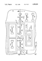
- An insulating layer 78 (FIG. 13) is deposited next (PSG or BPSG or equivalent), and contact holes (e.g. 79) opened, as shown in FIG. 13.
Landscapes
- Metal-Oxide And Bipolar Metal-Oxide Semiconductor Integrated Circuits (AREA)
- Element Separation (AREA)
Abstract
Description
              TABLE I
______________________________________
Hardness characteristics of thin-oxide notched regions
with degenerate regions in semiconductor region below it.
Pre-Rad       Post-Rad
t.sub.1
       ΔV.sub.t
                  30 KRADS       Δ1000 KRADS
A      (V)        V.sub.t
                         V.sub.t V.sub.t
                                      V.sub.t
______________________________________
1000    54        0.6     53      2    52
2000   107        2.5    104      9   105
3000   161        6.0    155     20   140
4000   215        10.0   205     34   180
5000   270        16.0   254     54   215
______________________________________
______________________________________
t.sub.2
______________________________________
 8000   29       -40.0   <0      -140  <0
10000   37       -63.0   <0      -215  <0
12000   44       -90.0   <0      -310  <0
______________________________________
Claims (6)
Priority Applications (1)
| Application Number | Priority Date | Filing Date | Title |
|---|---|---|---|
| US07/130,914 US4990983A (en) | 1986-10-31 | 1987-12-07 | Radiation hardened field oxides for NMOS and CMOS-bulk and process for forming |
Applications Claiming Priority (2)
| Application Number | Priority Date | Filing Date | Title |
|---|---|---|---|
| US92631986A | 1986-10-31 | 1986-10-31 | |
| US07/130,914 US4990983A (en) | 1986-10-31 | 1987-12-07 | Radiation hardened field oxides for NMOS and CMOS-bulk and process for forming |
Related Parent Applications (1)
| Application Number | Title | Priority Date | Filing Date |
|---|---|---|---|
| US92631986A Division | 1986-10-31 | 1986-10-31 |
Publications (1)
| Publication Number | Publication Date |
|---|---|
| US4990983A true US4990983A (en) | 1991-02-05 |
Family
ID=26828968
Family Applications (1)
| Application Number | Title | Priority Date | Filing Date |
|---|---|---|---|
| US07/130,914 Expired - Fee Related US4990983A (en) | 1986-10-31 | 1987-12-07 | Radiation hardened field oxides for NMOS and CMOS-bulk and process for forming |
Country Status (1)
| Country | Link |
|---|---|
| US (1) | US4990983A (en) |
Cited By (9)
| Publication number | Priority date | Publication date | Assignee | Title |
|---|---|---|---|---|
| US5239195A (en) * | 1990-05-17 | 1993-08-24 | Hello S.A. | Mos transistor with high threshold voltage |
| US5422505A (en) * | 1990-10-17 | 1995-06-06 | Kabushiki Kaisha Toshiba | FET having gate insulating films whose thickness is different depending on portions |
| US5599728A (en) * | 1994-04-07 | 1997-02-04 | Regents Of The University Of California | Method of fabricating a self-aligned high speed MOSFET device |
| US5650654A (en) * | 1994-12-30 | 1997-07-22 | International Business Machines Corporation | MOSFET device having controlled parasitic isolation threshold voltage |
| US5670816A (en) * | 1989-04-07 | 1997-09-23 | Kabushiki Kaisha Toshiba | Semiconductor device |
| US5675171A (en) * | 1995-04-20 | 1997-10-07 | Nec Corporation | Integrated insulated gate field effect transistors with thin insulation region between field insulation regions |
| US6624495B2 (en) * | 1997-04-23 | 2003-09-23 | Altera Corporation | Adjustable threshold isolation transistor |
| US20040262641A1 (en) * | 1999-01-14 | 2004-12-30 | Rhodes Howard E. | Trench isolation for semiconductor devices |
| US9281232B2 (en) | 2013-10-21 | 2016-03-08 | Texas Instruments Incorporated | Device having improved radiation hardness and high breakdown voltages |
Citations (11)
| Publication number | Priority date | Publication date | Assignee | Title |
|---|---|---|---|---|
| US3450960A (en) * | 1965-09-29 | 1969-06-17 | Ibm | Insulated-gate field effect transistor with nonplanar gate electrode structure for optimizing transconductance |
| US3751722A (en) * | 1971-04-30 | 1973-08-07 | Standard Microsyst Smc | Mos integrated circuit with substrate containing selectively formed resistivity regions |
| US3892609A (en) * | 1971-10-07 | 1975-07-01 | Hughes Aircraft Co | Production of mis integrated devices with high inversion voltage to threshold voltage ratios |
| US3974516A (en) * | 1970-11-21 | 1976-08-10 | U.S. Philips Corporation | Method of manufacturing a semiconductor device having at least one insulated gate field effect transistor, and semiconductor device manufactured by using the method |
| JPS5237775A (en) * | 1975-09-19 | 1977-03-23 | Mitsubishi Electric Corp | Complementary semiconductor device |
| US4063274A (en) * | 1976-12-10 | 1977-12-13 | Rca Corporation | Integrated circuit device including both N-channel and P-channel insulated gate field effect transistors |
| JPS5651870A (en) * | 1979-10-05 | 1981-05-09 | Oki Electric Ind Co Ltd | Manufacture of complementary type mos semiconductor device |
| US4282648A (en) * | 1980-03-24 | 1981-08-11 | Intel Corporation | CMOS process |
| US4458262A (en) * | 1980-05-27 | 1984-07-03 | Supertex, Inc. | CMOS Device with ion-implanted channel-stop region and fabrication method therefor |
| US4613886A (en) * | 1981-07-09 | 1986-09-23 | Intel Corporation | CMOS static memory cell |
| US4748489A (en) * | 1985-03-22 | 1988-05-31 | Nec Corporation | Integrated circuit semiconductor device having improved isolation region |
-
1987
- 1987-12-07 US US07/130,914 patent/US4990983A/en not_active Expired - Fee Related
Patent Citations (11)
| Publication number | Priority date | Publication date | Assignee | Title |
|---|---|---|---|---|
| US3450960A (en) * | 1965-09-29 | 1969-06-17 | Ibm | Insulated-gate field effect transistor with nonplanar gate electrode structure for optimizing transconductance |
| US3974516A (en) * | 1970-11-21 | 1976-08-10 | U.S. Philips Corporation | Method of manufacturing a semiconductor device having at least one insulated gate field effect transistor, and semiconductor device manufactured by using the method |
| US3751722A (en) * | 1971-04-30 | 1973-08-07 | Standard Microsyst Smc | Mos integrated circuit with substrate containing selectively formed resistivity regions |
| US3892609A (en) * | 1971-10-07 | 1975-07-01 | Hughes Aircraft Co | Production of mis integrated devices with high inversion voltage to threshold voltage ratios |
| JPS5237775A (en) * | 1975-09-19 | 1977-03-23 | Mitsubishi Electric Corp | Complementary semiconductor device |
| US4063274A (en) * | 1976-12-10 | 1977-12-13 | Rca Corporation | Integrated circuit device including both N-channel and P-channel insulated gate field effect transistors |
| JPS5651870A (en) * | 1979-10-05 | 1981-05-09 | Oki Electric Ind Co Ltd | Manufacture of complementary type mos semiconductor device |
| US4282648A (en) * | 1980-03-24 | 1981-08-11 | Intel Corporation | CMOS process |
| US4458262A (en) * | 1980-05-27 | 1984-07-03 | Supertex, Inc. | CMOS Device with ion-implanted channel-stop region and fabrication method therefor |
| US4613886A (en) * | 1981-07-09 | 1986-09-23 | Intel Corporation | CMOS static memory cell |
| US4748489A (en) * | 1985-03-22 | 1988-05-31 | Nec Corporation | Integrated circuit semiconductor device having improved isolation region |
Cited By (16)
| Publication number | Priority date | Publication date | Assignee | Title |
|---|---|---|---|---|
| US5670816A (en) * | 1989-04-07 | 1997-09-23 | Kabushiki Kaisha Toshiba | Semiconductor device |
| US5239195A (en) * | 1990-05-17 | 1993-08-24 | Hello S.A. | Mos transistor with high threshold voltage |
| US5422505A (en) * | 1990-10-17 | 1995-06-06 | Kabushiki Kaisha Toshiba | FET having gate insulating films whose thickness is different depending on portions |
| US5599728A (en) * | 1994-04-07 | 1997-02-04 | Regents Of The University Of California | Method of fabricating a self-aligned high speed MOSFET device |
| US5650654A (en) * | 1994-12-30 | 1997-07-22 | International Business Machines Corporation | MOSFET device having controlled parasitic isolation threshold voltage |
| US5675171A (en) * | 1995-04-20 | 1997-10-07 | Nec Corporation | Integrated insulated gate field effect transistors with thin insulation region between field insulation regions |
| US6943072B2 (en) | 1997-04-23 | 2005-09-13 | Altera Corporation | Adjustable threshold isolation transistor |
| US6624495B2 (en) * | 1997-04-23 | 2003-09-23 | Altera Corporation | Adjustable threshold isolation transistor |
| US20040018698A1 (en) * | 1997-04-23 | 2004-01-29 | Altera Corporation | Adjustable threshold isolation transistor |
| US20040262641A1 (en) * | 1999-01-14 | 2004-12-30 | Rhodes Howard E. | Trench isolation for semiconductor devices |
| US6856001B2 (en) * | 1999-01-14 | 2005-02-15 | Micron Technology, Inc. | Trench isolation for semiconductor devices |
| US7071531B2 (en) | 1999-01-14 | 2006-07-04 | Micron Technology, Inc. | Trench isolation for semiconductor devices |
| US20060244015A1 (en) * | 1999-01-14 | 2006-11-02 | Rhodes Howard E | Trench isolation for semiconductor devices |
| US9281232B2 (en) | 2013-10-21 | 2016-03-08 | Texas Instruments Incorporated | Device having improved radiation hardness and high breakdown voltages |
| US9620586B2 (en) | 2013-10-21 | 2017-04-11 | Texas Instruments Incorporated | Device having improved radiation hardness and high breakdown voltages |
| US9653544B2 (en) | 2013-10-21 | 2017-05-16 | Texas Instruments Incorporated | Methods for fabricating radiation hardened MOS devices |
Similar Documents
| Publication | Publication Date | Title |
|---|---|---|
| US6538278B1 (en) | CMOS integrated circuit having PMOS and NMOS devices with different gate dielectric layers | |
| US4385947A (en) | Method for fabricating CMOS in P substrate with single guard ring using local oxidation | |
| US5763922A (en) | CMOS integrated circuit having PMOS and NMOS devices with different gate dielectric layers | |
| KR0173111B1 (en) | Trench Gate MOS FET | |
| US4574467A (en) | N- well CMOS process on a P substrate with double field guard rings and a PMOS buried channel | |
| US5137837A (en) | Radiation-hard, high-voltage semiconductive device structure fabricated on SOI substrate | |
| US4637124A (en) | Process for fabricating semiconductor integrated circuit device | |
| US4891326A (en) | Semiconductor device and a process for manufacturing the same | |
| US5970338A (en) | Method of producing an EEPROM semiconductor structure | |
| JPH0691201B2 (en) | Method for manufacturing CMOS semiconductor device | |
| KR100397096B1 (en) | Semiconductor device and manufacturing method thereof | |
| WO2001037333A1 (en) | Method of fabrication dual threshold voltage n-channel and p-channel mosfets with a single extra masked implant operation | |
| US4994407A (en) | Radiation hardened field oxides for NMOS and CMOS-bulk and process for forming | |
| US5543338A (en) | Method for manufacturing a semiconductor device using a semiconductor-on-insulator substrate | |
| US4990983A (en) | Radiation hardened field oxides for NMOS and CMOS-bulk and process for forming | |
| US5506438A (en) | Semiconductor device with two different threshold voltages | |
| US4682408A (en) | Method for making field oxide region with self-aligned channel stop implantation | |
| KR890004797B1 (en) | MIS type semiconductor device formed on semiconductor substrate having well region | |
| JPS60100469A (en) | Semiconductor device | |
| JP2001085533A (en) | Semiconductor device and manufacturing method thereof | |
| JPH05865B2 (en) | ||
| US5486482A (en) | Process for fabricating metal-gate CMOS transistor | |
| KR0166991B1 (en) | Method of manufacturing a semiconductor device provided with an isolation region | |
| JPH01155654A (en) | complementary integrated circuit | |
| JPS62262462A (en) | Semiconductor device |
Legal Events
| Date | Code | Title | Description |
|---|---|---|---|
| CC | Certificate of correction | ||
| FEPP | Fee payment procedure |
Free format text: PAYOR NUMBER ASSIGNED (ORIGINAL EVENT CODE: ASPN); ENTITY STATUS OF PATENT OWNER: LARGE ENTITY |
|
| FPAY | Fee payment |
Year of fee payment: 4 |
|
| REMI | Maintenance fee reminder mailed | ||
| FPAY | Fee payment |
Year of fee payment: 8 |
|
| SULP | Surcharge for late payment | ||
| AS | Assignment |
Owner name: CREDIT SUISSE FIRST BOSTON, NEW YORK Free format text: SECURITY INTEREST;ASSIGNORS:CONEXANT SYSTEMS, INC.;BROOKTREE CORPORATION;BROOKTREE WORLDWIDE SALES CORPORATION;AND OTHERS;REEL/FRAME:009719/0537 Effective date: 19981221 |
|
| AS | Assignment |
Owner name: CONEXANT SYSTEMS, INC., CALIFORNIA Free format text: ASSIGNMENT OF ASSIGNORS INTEREST;ASSIGNOR:ROCKWELL SCIENCE CENTER, LLC;REEL/FRAME:010415/0761 Effective date: 19981210 |
|
| AS | Assignment |
Owner name: CONEXANT SYSTEMS, INC., CALIFORNIA Free format text: RELEASE OF SECURITY INTEREST;ASSIGNOR:CREDIT SUISSE FIRST BOSTON;REEL/FRAME:012252/0413 Effective date: 20011018 Owner name: BROOKTREE CORPORATION, CALIFORNIA Free format text: RELEASE OF SECURITY INTEREST;ASSIGNOR:CREDIT SUISSE FIRST BOSTON;REEL/FRAME:012252/0413 Effective date: 20011018 Owner name: BROOKTREE WORLDWIDE SALES CORPORATION, CALIFORNIA Free format text: RELEASE OF SECURITY INTEREST;ASSIGNOR:CREDIT SUISSE FIRST BOSTON;REEL/FRAME:012252/0413 Effective date: 20011018 Owner name: CONEXANT SYSTEMS WORLDWIDE, INC., CALIFORNIA Free format text: RELEASE OF SECURITY INTEREST;ASSIGNOR:CREDIT SUISSE FIRST BOSTON;REEL/FRAME:012252/0413 Effective date: 20011018 |
|
| LAPS | Lapse for failure to pay maintenance fees | ||
| FP | Lapsed due to failure to pay maintenance fee |
Effective date: 20030205 |
|
| STCH | Information on status: patent discontinuation |
Free format text: PATENT EXPIRED DUE TO NONPAYMENT OF MAINTENANCE FEES UNDER 37 CFR 1.362 |