US4985627A - Spin-polarized scanning tunneling microscope - Google Patents
Spin-polarized scanning tunneling microscope Download PDFInfo
- Publication number
- US4985627A US4985627A US07/391,908 US39190889A US4985627A US 4985627 A US4985627 A US 4985627A US 39190889 A US39190889 A US 39190889A US 4985627 A US4985627 A US 4985627A
- Authority
- US
- United States
- Prior art keywords
- sample
- tunnel tip
- light beam
- microscope
- tip
- Prior art date
- Legal status (The legal status is an assumption and is not a legal conclusion. Google has not performed a legal analysis and makes no representation as to the accuracy of the status listed.)
- Expired - Lifetime
Links
Images
Classifications
-
- G—PHYSICS
- G01—MEASURING; TESTING
- G01Q—SCANNING-PROBE TECHNIQUES OR APPARATUS; APPLICATIONS OF SCANNING-PROBE TECHNIQUES, e.g. SCANNING PROBE MICROSCOPY [SPM]
- G01Q60/00—Particular types of SPM [Scanning Probe Microscopy] or microscopes; Essential components thereof
- G01Q60/10—STM [Scanning Tunnelling Microscopy] or apparatus therefor, e.g. STM probes
- G01Q60/16—Probes, their manufacture, or their related instrumentation, e.g. holders
-
- B—PERFORMING OPERATIONS; TRANSPORTING
- B82—NANOTECHNOLOGY
- B82Y—SPECIFIC USES OR APPLICATIONS OF NANOSTRUCTURES; MEASUREMENT OR ANALYSIS OF NANOSTRUCTURES; MANUFACTURE OR TREATMENT OF NANOSTRUCTURES
- B82Y35/00—Methods or apparatus for measurement or analysis of nanostructures
-
- G—PHYSICS
- G01—MEASURING; TESTING
- G01Q—SCANNING-PROBE TECHNIQUES OR APPARATUS; APPLICATIONS OF SCANNING-PROBE TECHNIQUES, e.g. SCANNING PROBE MICROSCOPY [SPM]
- G01Q60/00—Particular types of SPM [Scanning Probe Microscopy] or microscopes; Essential components thereof
- G01Q60/50—MFM [Magnetic Force Microscopy] or apparatus therefor, e.g. MFM probes
- G01Q60/54—Probes, their manufacture, or their related instrumentation, e.g. holders
- G01Q60/56—Probes with magnetic coating
-
- Y—GENERAL TAGGING OF NEW TECHNOLOGICAL DEVELOPMENTS; GENERAL TAGGING OF CROSS-SECTIONAL TECHNOLOGIES SPANNING OVER SEVERAL SECTIONS OF THE IPC; TECHNICAL SUBJECTS COVERED BY FORMER USPC CROSS-REFERENCE ART COLLECTIONS [XRACs] AND DIGESTS
- Y10—TECHNICAL SUBJECTS COVERED BY FORMER USPC
- Y10S—TECHNICAL SUBJECTS COVERED BY FORMER USPC CROSS-REFERENCE ART COLLECTIONS [XRACs] AND DIGESTS
- Y10S977/00—Nanotechnology
- Y10S977/84—Manufacture, treatment, or detection of nanostructure
- Y10S977/849—Manufacture, treatment, or detection of nanostructure with scanning probe
- Y10S977/86—Scanning probe structure
- Y10S977/861—Scanning tunneling probe
Definitions
- the present invention relates to scanning funneling microscopes which by means of optically induced spin polarization measure the magnetic properties of surfaces.
- Scanning tunneling microscopy per se is well known in the art to permit the inspection of surface topographies down to the atomic level, based on the strong dependency of the tunneling current upon the distance of the tunnel tip from the surface being investigated.
- a summary of the features of scanning tunneling microscopy is provided by the inventors of the Scanning Tunneling Microscope, G. Binnig and H. Rohrer, "Scanning Tunneling Microscopy", IBM Journal of Research and Development, Vol. 30, No. 4, July 1986, pp. 355-369, where a useful catalogue of relevant literature published prior to 1986 is provided.
- the tip of a scanning tunneling microscope closely follows the profile of the surface under investigation by monitoring the tunneling current and providing a feedback signal dependent on the deviation of the distance between the tip and surface from a predetermined value.
- a feedback signal dependent on the deviation of the distance between the tip and surface from a predetermined value.
- Qualitative information at comparable resolution i.e. information regarding the chemical elements present at (or near) the surface of a specimen may be obtained from a field-emission scanning Auger electron microscope of the type described in EP-A-1-0 189 498.
- the energy of the Auger electrons emitted by a material hit by a sharply focused field-emitted electron beam is characteristic of the emitting element.
- a principal object of the present invention is therefore, the provision of a scanning tunneling microscope in which spin-polarization is employed to detect the magnetic properties of a material at the point of impingement of a spin-polarized electron beam.
- a spin-polarized scanning tunneling microscope comprising a tunnel tip disposed opposite the surface of a sample to be investigated separated by a gap having a width between 0.1 and 10 nm, an xyz-drive for positioning the tunnel tip at the gap and for causing the tunnel tip to be raster-scanned across the sample surface, and electronic circuitry for maintaining the width of said gap essentially constant.
- the scanning tunneling microscope is characterized in that the tunnel tip and the sample to be investigated comprise, at least in part, different materials, one of the materials being a magnetic material, the other being a semiconductor material, and a light source is provided for emitting a beam of polarized light, the light beam made to impinge upon said surface at a point closest to the apex of the tunnel tip.
- FIG. 1 is a schematic energy diagram of the tunnel region for a p-doped GaAs sample and a magnetic tip;
- FIG. 2 illustrates an embodiment of a scanning tunneling microscope in accordance with the present invention
- FIG. 3 illustrates an alternative embodiment of a scanning tunneling microscope in accordance with the present invention
- FIG. 4 illustrates another alternative embodiment of a scanning tunneling microscope in accordance with the present invention.
- FIG. 5 is a schematic block diagram of the components comprising the scanning tunneling microscope in accordance with the invention.
- the present invention is based on the knowledge that tunneling microscopy is feasible with optionally oriented spin-polarized electrons between a semiconductor and a magnetically conducting material. This involves spin-polarized conduction electrons, and/or valence holes, the polarization vector of which can be modulated by optical means, on one side of the tunnel barrier, and a magnetic material on the other.
- the order of magnitude of the currents to be expected is exemplified by a photoexcited tunneling current of about 10 nA having been measured between a gold tip and a gallium arsenide (110) surface.
- sources of polarized electrons compounds of the III/V, II/IV/V, II/III/VI groups of elements, and other semiconductors generally having a large valence band spin-orbit splitting and a long carrier diffusion length are preferred.
- up/down spin-polarized electrons can be photoexcited into the conduction band by right/left circularly polarized light.
- F. Meier and B.P. Zakharchenya ed.
- Optical Orientation North-Holland 1984, p. 486.
- d is the barrier width, i.e. the distance between the tip and the surface, ⁇ having a value of ⁇ (0 ⁇ 1 eV) which largely depends on the finish of the surface of the III-V compound is the band bending, L is the depletion zone depth ( ⁇ 5 . . .
- I ss is the surface state tunneling current
- I+,I- are the tunneling currents excited by right or left polarized light, respectively
- CB designates the conduction band
- VB designates the valence band
- E f is the Fermi energy
- the tunneling currents I+,I- resulting from the impingement of the ⁇ +, ⁇ - polarized photon beam are related to the magnetization of the ferromagnetic material by the asymmetry term ##EQU1## wherein I b is the background tunneling current due to thermal excitations, and which is exponentially small in a finite range around zero tunneling voltage.
- the current I b is independent of the helicity, i.e. rotary direction of polarization, of the exciting light.
- the currents, I b as well as I+,I- can contain surface state contributions I s which could change due to photoexcited electrons falling into surface states of the semiconductor prior to tunneling. In such as case, I s + ⁇ I s -. This effect can modify, and even enhance the tunnel asymmetry.
- the magnetic tip beyond the gap has an energy on the Fermi level with a majority spin-up magnetization.
- topography measurement by either constant current or constant tip-to-sample distance is possible during spin polarized tunneling.
- the tunneling current asymmetry will arise from the spin-polarization of both the sample and tip, and from their coupling via spin-conserving wave-function matching across the potential barrier.
- the proportionality of I+,I- to the total spin-up/down densities of states is in general not expected to be restored by the matching of the wave-functions. Indeed, those densities, as well as the polarization inside the magnet, are dominated by d or f wave-function components, whereas I+,I- are determined by the overlap of usually less polarized wave-function tails or, to a good approximation, by the product of suitably weighted local densities of states.
- the latter can in turn be estimated from separate measurements, namely the spin-polarized photoelectron escape from the semiconductor, and the inverse photoemission from the magnet, respectively.
- the asymmetry A t can be estimated from the product P c ⁇ P m . cos ⁇ , where P c is the polarization of the conduction electrons reaching the tunneling region, P m is the polarization of electrons tunneling into the empty magnetic states near the Fermi level of the magnet, and ⁇ is the angle between P c and P m . Approximating P c by its value for photoexcited GaAs(100), P c ⁇ 0.3, and P m by its value determined from polarized isochromat spectroscopy measurements.
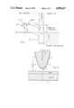
- a tunnel tip 3 comprising magnetic material.
- the magnetic material used can be in whisker form, such as iron, or magnetic material evaporated onto a tungsten tip, or onto an optionally transparent crystal.
- the exciting light beam 4 having an energy of h ⁇ enters from the back into tunnel tip 3.
- This mode of operation obviously requires an optically transparent tip, comprising, e.g., crystal material coated with a very thin metal layer 5, such as iron. With the thickness envisioned for this purpose, iron layer 5 may still be considered transparent to a laser beam.
- a voltage source 6, connected between semiconductor layer 1 and tip 3 provides the necessary tunneling voltage across gap 7. With this arrangement, the spin-polarization effect due to surface states, both intrinsic and/or related to defects, steps, adsorbates, etc., on the semiconductor surface is possible.
- the optimum wave length of the laser light beam used in connection with the invention depends on the chemistry of the semiconductors employed.
- the wavelength ⁇ should be in the range between 690 nm ⁇ 820 nm.
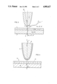
- FIG. 3 shows substantially the same arrangement as FIG. 2, with either of two differences.
- the first difference is when the exciting light beam 8 is transmitted from below (as shown) through the semiconductor layer 1 (and substrate 2, if any) and the second difference is when the light beam 9 impinges onto the surface of the semiconductor layer 1 at an angle on incidence ⁇ from the normal axis.
- Tip 10 comprises optically transparent material, such as glass, for example, and is coated with a thin layer 11 of gallium arsenide. Tip 10 is placed close to the surface of a magnetic medium 12, such as a magnetic film 13 disposed on a substrate 14. Again, as described above, there are three modes of operation. The optical energy h ⁇ is supplied (1) through tip 10 from the back, (2) from the side at an angle of incidence ⁇ (now shown), and (3) from underneath magnetic film 13, respectively. With any one of these three modes, the domain structure of the magnetic surface may be investigated with unprecedented resolution.
- a magnetic medium 12 such as a magnetic film 13 disposed on a substrate 14.
- optical orientation is that the direction of the spin-polarization vector P o can be controlled via the helicity of the exciting light, as well as by the angle of incidence ⁇ of the light beam.
- optical excitation through tip 10 or through the flat surface is necessary. In all cases, rapid modulation of either control parameter together with phase-sensitive detection is of the essence.
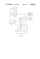
- FIG. 5 shows a schematic block diagram with the arrangement of the circuitry and building blocks of a scanning tunneling microscope in accordance with the present invention.
- Tunnel tip 15 is position-controlled by an xyz-drive 16 which is fixed to a frame 17 of a table 18 upon which table the sample to be inspected is disposed.
- xyz-drive 16 controls the relative position of tunnel tip 15 with respect to sample 19 such that the distance between tip 15 and the surface of sample 19 is kept constant by means of a feedback signal from conventional STM electronics 20.
- tip 15 is of the transparent type, and the circuitry polarized light beam 21 enters the back of tip 15.
- the light beam is generated by a laser 22 and passed through a modulator 23 which causes the light beam to be right- or left-polarized in accordance with a signal received from a waveform generator 24.
- a lens and mirror system 25 serves to direct the light beam to the back of tunnel tip 15.
- phase-sensitive detector 26 Also connected to the output of waveform generator 24 is the input of a phase-sensitive detector 26.
- the detector 26 receives a second input signal from tunnel tip 15.
- the function of detector 26 may also be performed through gating or by means of digital electronics.
- a display unit 27 is connected to the STM electronics 20 and to said phase-sensitive detector 26.
- the detector 26 also receives an input signal from STM electronics 20.
Landscapes
- Nuclear Medicine, Radiotherapy & Molecular Imaging (AREA)
- Physics & Mathematics (AREA)
- Health & Medical Sciences (AREA)
- General Health & Medical Sciences (AREA)
- General Physics & Mathematics (AREA)
- Radiology & Medical Imaging (AREA)
- Chemical & Material Sciences (AREA)
- Engineering & Computer Science (AREA)
- Nanotechnology (AREA)
- Analytical Chemistry (AREA)
- Crystallography & Structural Chemistry (AREA)
- Measurement Of Length, Angles, Or The Like Using Electric Or Magnetic Means (AREA)
- Measuring Magnetic Variables (AREA)
Abstract
Description
Claims (7)
Applications Claiming Priority (2)
| Application Number | Priority Date | Filing Date | Title |
|---|---|---|---|
| EP88810570A EP0355241A1 (en) | 1988-08-18 | 1988-08-18 | Spin-polarized scanning tunneling microscope |
| EP88810570.7 | 1988-08-18 |
Publications (1)
| Publication Number | Publication Date |
|---|---|
| US4985627A true US4985627A (en) | 1991-01-15 |
Family
ID=8200598
Family Applications (1)
| Application Number | Title | Priority Date | Filing Date |
|---|---|---|---|
| US07/391,908 Expired - Lifetime US4985627A (en) | 1988-08-18 | 1989-08-10 | Spin-polarized scanning tunneling microscope |
Country Status (3)
| Country | Link |
|---|---|
| US (1) | US4985627A (en) |
| EP (1) | EP0355241A1 (en) |
| JP (1) | JPH02176482A (en) |
Cited By (22)
| Publication number | Priority date | Publication date | Assignee | Title |
|---|---|---|---|---|
| US5107555A (en) * | 1990-12-12 | 1992-04-28 | Thrasher Mickey L | Crib rocking assembly |
| US5138159A (en) * | 1990-07-20 | 1992-08-11 | Olympus Optical Co., Ltd. | Scanning tunneling microscope |
| US5155412A (en) * | 1991-05-28 | 1992-10-13 | International Business Machines Corporation | Method for selectively scaling a field emission electron gun and device formed thereby |
| US5198667A (en) * | 1991-12-20 | 1993-03-30 | The United States Of America As Represented By The Secretary Of The Navy | Method and apparatus for performing scanning tunneling optical absorption spectroscopy |
| US5200936A (en) * | 1990-01-09 | 1993-04-06 | International Business Machines Corporation | Magneto-optic method and apparatus for recording and retrieving high-density digital data |
| US5260824A (en) * | 1989-04-24 | 1993-11-09 | Olympus Optical Co., Ltd. | Atomic force microscope |
| US5266801A (en) * | 1989-06-05 | 1993-11-30 | Digital Instruments, Inc. | Jumping probe microscope |
| US5343460A (en) * | 1990-08-03 | 1994-08-30 | Canon Kabushiki Kaisha | Information processing device and information processing method |
| US5436448A (en) * | 1992-01-10 | 1995-07-25 | Hitachi, Ltd. | Surface observing apparatus and method |
| US5446687A (en) * | 1994-01-31 | 1995-08-29 | Terastore, Inc. | Data storage medium for storing data as a polarization of a data magnetic field and method and apparatus using spin-polarized electrons for storing the data onto the data storage medium and reading the stored data therefrom |
| US5463897A (en) * | 1993-08-17 | 1995-11-07 | Digital Instruments, Inc. | Scanning stylus atomic force microscope with cantilever tracking and optical access |
| US5523572A (en) * | 1991-05-02 | 1996-06-04 | Daido Tokushuko Kabushiki Kaisha | Process of emitting highly spin-polarized electron beam and semiconductor device therefor |
| US5546337A (en) * | 1994-01-31 | 1996-08-13 | Terastore, Inc. | Method and apparatus for storing data using spin-polarized electrons |
| US5708327A (en) * | 1996-06-18 | 1998-01-13 | National Semiconductor Corporation | Flat panel display with magnetic field emitter |
| US5793743A (en) * | 1993-11-03 | 1998-08-11 | International Business Machines Corporation | Reading a magnetic storage medium with a probe that detects tunneling current induced in a magnetic layer by a non-ionizing light beam |
| US5796102A (en) * | 1993-09-17 | 1998-08-18 | Stichting Katholieke Universiteit Nijmegen | Measuring device for measuring the intensity and/or polarization of electromagnetic radiation, for determining physical properties of a preparation, and for reading information from a storage medium |
| US6002131A (en) * | 1998-03-25 | 1999-12-14 | The Board Of Trustees Of The Leland Stanford Junior University | Scanning probe potentiometer |
| DE19912814A1 (en) * | 1999-03-22 | 2000-10-19 | Max Planck Gesellschaft | Raster tunneling microscope images magnetic structure of test samples |
| US6304481B1 (en) | 1994-01-31 | 2001-10-16 | Terastore, Inc. | Method and apparatus for storing data using spin-polarized electrons |
| US20020149362A1 (en) * | 2001-03-05 | 2002-10-17 | Koichi Mukasa | Scanning magnetism detector and probe |
| US20040165482A1 (en) * | 2002-10-14 | 2004-08-26 | Samsung Electronics Co., Ltd. | Magnetic medium using spin-polarized electrons and apparatus and method of recording data on the magnetic medium |
| US20080073554A1 (en) * | 2006-05-19 | 2008-03-27 | Tsinghua University | Spin-polarized electron source and spin-polarized scanning tunneling microscope |
Families Citing this family (6)
| Publication number | Priority date | Publication date | Assignee | Title |
|---|---|---|---|---|
| EP0437275B1 (en) * | 1990-01-11 | 1997-08-27 | Canon Kabushiki Kaisha | Microprobe, method for producing the same, and information input and/or output apparatus utilizing the same |
| US5900729A (en) * | 1997-03-20 | 1999-05-04 | International Business Machines Corporation | Magnetic force microscopy probe with integrated coil |
| JP3399841B2 (en) * | 1998-06-25 | 2003-04-21 | 科学技術振興事業団 | Probe with optical waveguide and method of manufacturing the same |
| JP3557459B2 (en) * | 2001-06-26 | 2004-08-25 | 北海道大学長 | Scanning probe microscope |
| FR2886407B1 (en) * | 2005-05-27 | 2007-09-28 | Thales Sa | LOCAL INJECTOR OF POLARIZED ELECTRON SPIN WITH SEMICONDUCTOR POINT UNDER LIGHT EXCITATION |
| GB0619701D0 (en) * | 2006-10-05 | 2006-11-15 | Isis Innovation | Scanning tunnelling microscope |
Citations (4)
| Publication number | Priority date | Publication date | Assignee | Title |
|---|---|---|---|---|
| EP0027517A1 (en) * | 1979-09-20 | 1981-04-29 | International Business Machines Corporation | Scanning apparatus for surface analysis using vacuum-tunnel effect at cryogenic temperatures |
| JPS62139240A (en) * | 1985-12-13 | 1987-06-22 | Hitachi Ltd | scanning tunneling microscope |
| EP0272178A1 (en) * | 1986-11-27 | 1988-06-22 | Commissariat A L'energie Atomique | Spin-polarized electron source using a multiple microtip emission cathode, use in electron matter or electron particle interaction physics, plasma physics, electron microscopy |
| US4837435A (en) * | 1987-06-25 | 1989-06-06 | Seiko Instruments Inc. | Tunneling scanning microscope having light source |
Family Cites Families (1)
| Publication number | Priority date | Publication date | Assignee | Title |
|---|---|---|---|---|
| JPS60185145A (en) * | 1985-02-01 | 1985-09-20 | Hitachi Ltd | Spin polarizing electron source |
-
1988
- 1988-08-18 EP EP88810570A patent/EP0355241A1/en not_active Withdrawn
-
1989
- 1989-07-27 JP JP1192794A patent/JPH02176482A/en active Pending
- 1989-08-10 US US07/391,908 patent/US4985627A/en not_active Expired - Lifetime
Patent Citations (5)
| Publication number | Priority date | Publication date | Assignee | Title |
|---|---|---|---|---|
| EP0027517A1 (en) * | 1979-09-20 | 1981-04-29 | International Business Machines Corporation | Scanning apparatus for surface analysis using vacuum-tunnel effect at cryogenic temperatures |
| US4343993A (en) * | 1979-09-20 | 1982-08-10 | International Business Machines Corporation | Scanning tunneling microscope |
| JPS62139240A (en) * | 1985-12-13 | 1987-06-22 | Hitachi Ltd | scanning tunneling microscope |
| EP0272178A1 (en) * | 1986-11-27 | 1988-06-22 | Commissariat A L'energie Atomique | Spin-polarized electron source using a multiple microtip emission cathode, use in electron matter or electron particle interaction physics, plasma physics, electron microscopy |
| US4837435A (en) * | 1987-06-25 | 1989-06-06 | Seiko Instruments Inc. | Tunneling scanning microscope having light source |
Cited By (31)
| Publication number | Priority date | Publication date | Assignee | Title |
|---|---|---|---|---|
| US5260824A (en) * | 1989-04-24 | 1993-11-09 | Olympus Optical Co., Ltd. | Atomic force microscope |
| US5266801A (en) * | 1989-06-05 | 1993-11-30 | Digital Instruments, Inc. | Jumping probe microscope |
| US5415027A (en) * | 1989-06-05 | 1995-05-16 | Digital Instruments, Inc. | Jumping probe microscope |
| US5200936A (en) * | 1990-01-09 | 1993-04-06 | International Business Machines Corporation | Magneto-optic method and apparatus for recording and retrieving high-density digital data |
| US5138159A (en) * | 1990-07-20 | 1992-08-11 | Olympus Optical Co., Ltd. | Scanning tunneling microscope |
| US5343460A (en) * | 1990-08-03 | 1994-08-30 | Canon Kabushiki Kaisha | Information processing device and information processing method |
| US5107555A (en) * | 1990-12-12 | 1992-04-28 | Thrasher Mickey L | Crib rocking assembly |
| US5523572A (en) * | 1991-05-02 | 1996-06-04 | Daido Tokushuko Kabushiki Kaisha | Process of emitting highly spin-polarized electron beam and semiconductor device therefor |
| US5155412A (en) * | 1991-05-28 | 1992-10-13 | International Business Machines Corporation | Method for selectively scaling a field emission electron gun and device formed thereby |
| US5198667A (en) * | 1991-12-20 | 1993-03-30 | The United States Of America As Represented By The Secretary Of The Navy | Method and apparatus for performing scanning tunneling optical absorption spectroscopy |
| US5436448A (en) * | 1992-01-10 | 1995-07-25 | Hitachi, Ltd. | Surface observing apparatus and method |
| US5463897A (en) * | 1993-08-17 | 1995-11-07 | Digital Instruments, Inc. | Scanning stylus atomic force microscope with cantilever tracking and optical access |
| US5796102A (en) * | 1993-09-17 | 1998-08-18 | Stichting Katholieke Universiteit Nijmegen | Measuring device for measuring the intensity and/or polarization of electromagnetic radiation, for determining physical properties of a preparation, and for reading information from a storage medium |
| US5793743A (en) * | 1993-11-03 | 1998-08-11 | International Business Machines Corporation | Reading a magnetic storage medium with a probe that detects tunneling current induced in a magnetic layer by a non-ionizing light beam |
| US5604706A (en) * | 1994-01-31 | 1997-02-18 | Terastore, Inc. | Data storage medium for storing data as a polarization of a data magnetic field and method and apparatus using spin-polarized electrons for storing the data onto the data storage medium and reading the stored data therefrom |
| US6304481B1 (en) | 1994-01-31 | 2001-10-16 | Terastore, Inc. | Method and apparatus for storing data using spin-polarized electrons |
| US5546337A (en) * | 1994-01-31 | 1996-08-13 | Terastore, Inc. | Method and apparatus for storing data using spin-polarized electrons |
| US5446687A (en) * | 1994-01-31 | 1995-08-29 | Terastore, Inc. | Data storage medium for storing data as a polarization of a data magnetic field and method and apparatus using spin-polarized electrons for storing the data onto the data storage medium and reading the stored data therefrom |
| US5838020A (en) * | 1994-01-31 | 1998-11-17 | Terastore, Inc. | Method and apparatus for storing data using spin-polarized electrons |
| US6147894A (en) * | 1994-01-31 | 2000-11-14 | Terastore, Inc. | Method and apparatus for storing data using spin-polarized electrons |
| US5708327A (en) * | 1996-06-18 | 1998-01-13 | National Semiconductor Corporation | Flat panel display with magnetic field emitter |
| US6002131A (en) * | 1998-03-25 | 1999-12-14 | The Board Of Trustees Of The Leland Stanford Junior University | Scanning probe potentiometer |
| DE19912814C2 (en) * | 1999-03-22 | 2002-02-14 | Max Planck Gesellschaft | Method and device for scanning tunneling microscopy |
| DE19912814A1 (en) * | 1999-03-22 | 2000-10-19 | Max Planck Gesellschaft | Raster tunneling microscope images magnetic structure of test samples |
| US6476386B1 (en) | 1999-03-22 | 2002-11-05 | Max-Planck- Gesselschaft Zur Forderung Der Wissenschaften E.V. | Method and device for tunnel microscopy |
| US20020149362A1 (en) * | 2001-03-05 | 2002-10-17 | Koichi Mukasa | Scanning magnetism detector and probe |
| US6750450B2 (en) * | 2001-03-05 | 2004-06-15 | Hokkaido University | Scanning magnetism detector and probe |
| US20040165482A1 (en) * | 2002-10-14 | 2004-08-26 | Samsung Electronics Co., Ltd. | Magnetic medium using spin-polarized electrons and apparatus and method of recording data on the magnetic medium |
| US8553517B2 (en) * | 2002-10-14 | 2013-10-08 | Samsung Electronics Co., Ltd. | Magnetic medium using spin-polarized electrons and apparatus and method of recording data on the magnetic medium |
| US20080073554A1 (en) * | 2006-05-19 | 2008-03-27 | Tsinghua University | Spin-polarized electron source and spin-polarized scanning tunneling microscope |
| US7459682B2 (en) | 2006-05-19 | 2008-12-02 | Tsinghua University | Spin-polarized electron source and spin-polarized scanning tunneling microscope |
Also Published As
| Publication number | Publication date |
|---|---|
| EP0355241A1 (en) | 1990-02-28 |
| JPH02176482A (en) | 1990-07-09 |
Similar Documents
| Publication | Publication Date | Title |
|---|---|---|
| US4985627A (en) | Spin-polarized scanning tunneling microscope | |
| Smolyaninov et al. | Near-field second harmonic generation from a rough metal surface | |
| Nogués et al. | Positive exchange bias in Fe F 2-Fe bilayers | |
| Daboo et al. | Vectorial magnetometry with the magneto-optic Kerr effect applied to Co/Cu/Co trilayer structures | |
| Schlickum et al. | Spin-polarized scanning tunneling microscope for imaging the in-plane magnetization | |
| Suzuki et al. | Magnetic domains of cobalt ultrathin films observed with a scanning tunneling microscope using optically pumped GaAs tips | |
| US20040239936A1 (en) | Surface corrugation enhanced magneto-optical indicator film | |
| WO1995012882A1 (en) | Method and apparatus for retrieving digital data from a magnetic storage medium | |
| EP0872707B1 (en) | Apparatus for measuring exchange force | |
| Kottler et al. | Dichroic imaging of magnetic domains with a scanning near-field optical microscope | |
| Buchner et al. | Anisotropic polar magneto-optic Kerr effect of ultrathin Fe/GaAs (001) layers due to interfacial spin-orbit interaction | |
| Safarov et al. | Near-field magneto-optics with polarization sensitive STOM | |
| JP2967172B1 (en) | Spin detection axis rotation type spin polarization scanning tunneling microscope | |
| Bertrand et al. | Imaging of magnetic domains with scanning tunneling optical microscopy | |
| JPH071687B2 (en) | Scanning tunneling microscope | |
| Suzuki et al. | Spin-sensitive scanning tunneling microscope using GaAs optically pumped tips | |
| Dickson et al. | High-resolution optical imaging of magnetic-domain structures | |
| Lacoste et al. | Faraday-rotation imaging by near-field optical microscopy | |
| Nabhan et al. | Ferromagnetic domains imaging with a spin-polarized STM using GaAs tips. | |
| Schumacher et al. | Propagation of a magnetic domain wall in the presence of AFM fabricated defects | |
| Vysokikh et al. | High Resolution Magneto-optical Microscopy of Bi: YIG-thin Films with Both Domains and Topography Characterization | |
| Guillet et al. | Electrical detection of magnetic circular dichroism: Application to magnetic microscopy in ultrathin ferromagnetic films | |
| Falicov | Optical Properties of Magnetic Surfaces, Interfaces, Thin Films, Overlayers, and Superlattices | |
| Güdde et al. | About the depth sensitivity of second-harmonic radiation in ultra-thin metal films | |
| JP2842000B2 (en) | Observation method of magnetic domain or magnetic structure using scanning tunneling microscope |
Legal Events
| Date | Code | Title | Description |
|---|---|---|---|
| AS | Assignment |
Owner name: INTERNATIONAL BUSINESS MACHINES CORPORATION, ARMON Free format text: ASSIGNMENT OF ASSIGNORS INTEREST.;ASSIGNORS:GUTIERREZ, SANTOS F. A.;BARATOFF, ALEXIS;POHL, WOLFGANG D.;REEL/FRAME:005109/0763 Effective date: 19890807 |
|
| STCF | Information on status: patent grant |
Free format text: PATENTED CASE |
|
| AS | Assignment |
Owner name: NIKON VENTURES CORPORATION, CALIFORNIA Free format text: SECURITY INTEREST;ASSIGNOR:PARK SCIENTIFIC INSTRUMENTS CORPORATION;REEL/FRAME:007078/0409 Effective date: 19940726 |
|
| REMI | Maintenance fee reminder mailed | ||
| FPAY | Fee payment |
Year of fee payment: 4 |
|
| SULP | Surcharge for late payment | ||
| AS | Assignment |
Owner name: SILICON VALLEY BANK, CALIFORNIA Free format text: SECURITY INTEREST;ASSIGNOR:PARK SCIENTIFIC INSTRUMENTS CORP.;REEL/FRAME:007773/0802 Effective date: 19970131 |
|
| FPAY | Fee payment |
Year of fee payment: 8 |
|
| FPAY | Fee payment |
Year of fee payment: 12 |