US4945066A - Process for manufacturing a dynamic random access memory cell - Google Patents
Process for manufacturing a dynamic random access memory cell Download PDFInfo
- Publication number
- US4945066A US4945066A US07/159,177 US15917788A US4945066A US 4945066 A US4945066 A US 4945066A US 15917788 A US15917788 A US 15917788A US 4945066 A US4945066 A US 4945066A
- Authority
- US
- United States
- Prior art keywords
- forming
- oxide layer
- storage capacitor
- transistor
- barrier
- Prior art date
- Legal status (The legal status is an assumption and is not a legal conclusion. Google has not performed a legal analysis and makes no representation as to the accuracy of the status listed.)
- Expired - Lifetime
Links
Images


Classifications
-
- H—ELECTRICITY
- H10—SEMICONDUCTOR DEVICES; ELECTRIC SOLID-STATE DEVICES NOT OTHERWISE PROVIDED FOR
- H10B—ELECTRONIC MEMORY DEVICES
- H10B12/00—Dynamic random access memory [DRAM] devices
- H10B12/01—Manufacture or treatment
- H10B12/02—Manufacture or treatment for one transistor one-capacitor [1T-1C] memory cells
- H10B12/03—Making the capacitor or connections thereto
- H10B12/033—Making the capacitor or connections thereto the capacitor extending over the transistor
- H10B12/0335—Making a connection between the transistor and the capacitor, e.g. plug
-
- H—ELECTRICITY
- H10—SEMICONDUCTOR DEVICES; ELECTRIC SOLID-STATE DEVICES NOT OTHERWISE PROVIDED FOR
- H10B—ELECTRONIC MEMORY DEVICES
- H10B12/00—Dynamic random access memory [DRAM] devices
- H10B12/30—DRAM devices comprising one-transistor - one-capacitor [1T-1C] memory cells
-
- H—ELECTRICITY
- H10—SEMICONDUCTOR DEVICES; ELECTRIC SOLID-STATE DEVICES NOT OTHERWISE PROVIDED FOR
- H10P—GENERIC PROCESSES OR APPARATUS FOR THE MANUFACTURE OR TREATMENT OF DEVICES COVERED BY CLASS H10
- H10P14/00—Formation of materials, e.g. in the shape of layers or pillars
- H10P14/40—Formation of materials, e.g. in the shape of layers or pillars of conductive or resistive materials
- H10P14/416—Formation of materials, e.g. in the shape of layers or pillars of conductive or resistive materials of highly doped semiconductor materials, e.g. polysilicon layers or amorphous silicon layers
-
- H—ELECTRICITY
- H10—SEMICONDUCTOR DEVICES; ELECTRIC SOLID-STATE DEVICES NOT OTHERWISE PROVIDED FOR
- H10P—GENERIC PROCESSES OR APPARATUS FOR THE MANUFACTURE OR TREATMENT OF DEVICES COVERED BY CLASS H10
- H10P30/00—Ion implantation into wafers, substrates or parts of devices
- H10P30/20—Ion implantation into wafers, substrates or parts of devices into semiconductor materials, e.g. for doping
Definitions
- This invention relates to a process for manufacturing a dynamic random access memory (DRAM) cell, and more particularly to such a process for manufacturing a DRAM cell wherein each DRAM cell is formed of a single transistor and a single capacitive storage device, and has a high capacitance.
- DRAM dynamic random access memory
- a memory cell having a combination of a single transistor coupled with a single capacitive device has been widely used, and the combination is referred to as a "single transistor cell" for which a folded bit line array is employed as illustrated in FIG. 1 showing a schematic circuit diagram of a single transistor DRAM cell array.
- a transistor Q is a NMOS transistor
- a bit line B is connected to a drain D of the transistor
- a word line W is connected to a gate G of the transistor
- a source of the transistor is connected to a storage capacitor C
- the other side of the capacitor is coupled to a silicon substrate.
- FIG. 2 a plan view showing the layout according to the circuit configuration of FIG. 1, the word line W represents a second polysilicon strip 50, the bit line B represents a metal strip 52 formed of aluminium and so on, a region 54 is a first polysilicon region for a storage capacitor and a region 60 is a N+ source region formed by an ion implantation of N-type impurities, said source region connecting with a conductive layer under the first polysilicon region 54 by way of a conductive layer below a mini-field oxide region 58.
- a region 62 is a drain region formed by an ion implantation of N-type impurities
- a region 56 is a gate region wherein a gate oxide is formed under the second polysilicon region and a portion under the oxide becomes a channel layer
- a window 64 is a metal-silicon connecting part for coupling the drain 62 and the bit line 52.
- the mini-field oxide layer 58 is formed at the same time that a surface insulating layer of the first polysilicon region 54 overlapped in the upper part of the capacitive region is formed, and arsenic (As) of an arsenic ion implantation layer in a silicon substrate surface below the storage capacitor region, which becomes an electrode of the storage capacitor, is diffused through a side diffusion into a silicon substrate surface below the mini-field oxide layer.
- the arsenic ion-implanted in the silicon substrate surface often fails to be diffused enough into the connecting part of the mini-field oxide layer and the source region of the transistor due to its low diffusion factor. Also, a decrease in the arsenic ion density arising from an out diffusion results in a high resistance between the capacitor and the transistor. Thus due to said decrease, a margin of supply voltage to a DRAM is reduced and refresh time is rapidly decreased, thereby resulting in an inability to perform a high-speed operation. Moreover, in the worst case, an open circuit in the connection between said capacitor and transistor often makes the manufacture of an entire chip a failure.
- Another problem is that there is increased possibility of a soft-error occurrence, wherein data "1" stored in the capacitor is changed into data "0" because the amount of electric charge is reduced in a storage region of minority carriers resulting from ⁇ (Alpha) particles which are generated from uranium-group substances of fabrication materials of memory chips, as a cell area and an electric charging amount stored in a cell are both reduced accommodate the density of to a large intergrated circuit of semiconductor memory devices.
- Another problem in the prior art is that there is also an increased a possibility of a soft-error occurrence by which the data "0” reads out to be the data "1", because, as the minority carriers generated by the ⁇ particle move to the N+ drain region of a transistor, the electric potential in a bit line goes down.
- the process comprises the steps of:
- FIG. 1 is a schematic circuit diagram of a single transistor DRAM cell array
- FIG. 2 is a plan view for the layout of the single transistor DRAM cell array
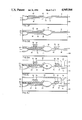
- FIGS. 3A to 3J are partial cross-sectional views showing each stage of manufacturing the single transistor memory cell in accordance with the invention.
- FIGS. 3A to 3J are cross sectional views taken through a cutting position a-a shown in FIG. 2 in a plate-shaped semiconductor body, showing each aspect of manufacturing the single transistor memory cell in accordance with the invention.
- a starting material is a P-type single crystal silicon substrate, wherein there is used a wafer more than 5 inches in diameter having an impurity density of 7 ⁇ 10 14 -3 ⁇ 10 15 /cm 3 and a ⁇ 100> direction in crystal lattice orientation.
- FIG. 3A showing a fabrication sequence for forming an oxide and a nitride on a surface of silicon substrate 100 and performing ion implantation for forming a channel stopping layer
- a silicon oxide layer 10 having a thickness of 150-500 ⁇ on the whole surface by means of a heat oxidation with a temperature of 950°-1050° C., after rinsing the P-type silicon substrate 100.
- a silicon nitride layer 12 having a thickness of 1000-1500 ⁇ is formed over all the oxide layer 10 in the ambient environment of Dichlorosilane (SiH2C12) and Ammonia (NH3) of a reactor, and a photoresist 13 is then coated over the silicon nitride layer.
- SiH2C12 Dichlorosilane
- NH3 Ammonia
- FIG. 3B shows a fabrication sequence for forming a field oxide layer 16 used to isolate each cell.
- the photoresist layer 13 there is removed the photoresist layer 13 and then formed the field oxide layer 16 having a thickness of 5000-6000 ⁇ in a steam or oxidation ambient environment and at a temperature of 900°-1000° C.
- the oxide layer 10 does not grow due to a masking effect of the silicon nitride layer 12.
- FIG. 3C shows a fabrication sequence of phosphorus ion implantation for coupling a lower electrode of a storage capacitor and a source area of a transistor below a mini-field, in which photoresist is coated, then exposed to the ultraviolet light through a masking material and further developed.
- an ion implantation of phosphorus ions is performed into the area 19 with an energy of 30-50 keV and a dose of 10 13 -10 14 /cm 2 by means of employing as a mask the silicon nitride 12 and photoresist 17 to form coupling 18.
- remaining photo resist is removed.
- FIG. 3D shows a fabrication sequence in which there is etched an edge part of the field oxide layer 16 just around the capacitor perimeter in order to form a high capacitive storage capacitor and boron is ion-implanted.
- photoresist is coated, then exposed to the ultraviolet light through a mask and developed.
- the exposed field oxide layer 16 and oxide layer 10 is etched for a time of 20-60 seconds at a temperature of 20°-30° C. in a diluted solution having a mixing ratio of Hydrofluoric acid (HF) to Deionized water (D.I. water) is 1:7.
- HF Hydrofluoric acid
- an ion implantation of boron ions is performed with an energy of 50-150 keV and a dose 5.0 ⁇ 10 12 -10 14 /cm 2 by means of employing the photoresist 20 as a mask to form barrier 22 against minority carrier resulting from alpha particles.
- the edge of said field oxide layer 16 is etched and the area of the storage capacitance enlarged, whereby capacitance of the storage capacitor is enlarged by 10-15% more than that of the prior art.
- FIG. 3E represents a fabrication sequence in which an oxide layer 23 is formed on an etched portion 21 of the storage capacitor and a lower electrode of the storage capacitor is formed.
- An oxide silicon layer 23 is at first formed in said etched portion 21 by using thermal oxidation and then an ion implantation of arsenic ions is performed to form a lower electrode 24 with an energy of 70-120 keV and a dose of 3 ⁇ 10 13 3 ⁇ 10 14 /cm 2 .
- FIG. 3F represents a fabrication step for a first polysilicon electrode 25 of the storage capacitor over said insulating layer 23.
- the polysilicon is at first coated over all the surface of the substrate in a thickness of 4000-6000 ⁇ within the reactor by means of a conventional processing method in the art and then deposited in a phosphorus oxychloride (POC13). After doping impurites so as to have a resistance of 20-80 ⁇ /square, there is coated a photoresist over all the surface of substrate. Then, using a photo lithography process, all the polysilicon is etched except for a portion to form gate 25 of the storage capacitor of the cell array and the remaining photoresist is removed.
- POC13 phosphorus oxychloride
- FIG. 3G is a fabrication step in which a thick oxide silicon layer is grown over the first polysilicon layer 25 for insulating a second polysilicon layer.
- a silicon oxide layer 27 is grown in the thickness of 2500-4500 ⁇ at a temperature of 900°-1000° C. using the thermal oxidation, and then the remaining silicon nitride layer 12 is all etched.
- the silicon oxide layer 27 there is formed a mini-field oxide layer 30, and the phosphorus or arsenic ion-implanted below the mini-field oxide layer is annealed by the thermal oxidation and simultaneously diffused. Therefore, a bird beak portion of the mini-field 30 is completely covered with phosphorus having a double side diffusion factor more than that of arsenic.
- boron ion implantation is performed on all the surface oxide, and in order to control a threshold voltage of a depletion MOS transistor, ion implantation of phosphorus or arsenic is performed.
- FIG. 3H is a fabrication step in which a second polysilicon layer for forming a gate electrode and a word of a MOS transistor is formed over said oxide layer, and arsenic ion-implantation is performed in order to form a drain area and a source area of the transistor.
- the second polysilicon layer 32 is coated over all the surface of said insulating layer by means of the conventional processing method and, then deposited in the POC13 and doped with impurities.
- a photoresist over all the surface of the substrate, a word line 32 is formed by using the photo lithography process and then ion-implanted with arsenic in order to form a source and a drain of the transistor.
- oxide layer 34 Over the second polysilicon layer 32, an oxide layer having a thickness of 1000-2500 ⁇ is grown by thermal oxidation.
- oxide layer 34 a diffusion of the arsenic ions implanted arises and, by this diffusion, there is formed source and drain area of the transistor.
- FIG. 3I is a fabrication step in which a passivation layer 38 is formed over the surface of the substrate formed through the aforementioned sequences and a barrier 40 against minority carriers resulting from alpha particles is also formed under the drain area 36.
- Interlayer oxide 38 which consists of Phospho Silicate Glass (PSG) or Borophospho silicate Glass (BPSG) covers all of the surface of the substrate shown in FIG. 3H by means of the conventional processing method. Then, after coating a photoresist on the surface, on which a window 39 is developed using photoresist and oxide etching for the formation of contact between a bit line and drain region by using the photo lithography method and the etch method.
- PSG Phospho Silicate Glass
- BPSG Borophospho silicate Glass
- the next step there is performed ion implantation of boron having an identical conductivity type to the substrate with an energy of 150-180 keV and a dose of 5 ⁇ 10 12 -5 ⁇ 10 13 /cm 2 without a separate etching process or a mask on all the surface of substrate.
- the boron ions are not deeply implanted into the area of the interlayer oxide, but they are deeply ion-implanted into the below part of the drain region 36 for the preparation of a region in which with boron ion implantations, a barrier is formed for retarding an injection of electrons generated from the substrate by ⁇ -particles.
- FIG. 3J represents a fabrication step for forming a bit line 42 of aluminium over the passivation layer 38.
- the connection with the source area is efficiently performed owing to the side diffusion of said impurities when forming the surface oxide of the first polysilicon layer.
- a margin of supply voltage and a refresh time in a DRAM device can be increased by reducing a resistance in a lower part of the mini-field oxide layer, and a capacitance of the storage capacitor can be enlarged by etching the edge part of the field oxide layer just around the capacitor perimeter.
Landscapes
- Engineering & Computer Science (AREA)
- Manufacturing & Machinery (AREA)
- Semiconductor Memories (AREA)
- Semiconductor Integrated Circuits (AREA)
Abstract
Description
Claims (19)
Applications Claiming Priority (2)
| Application Number | Priority Date | Filing Date | Title |
|---|---|---|---|
| KR1019870001554A KR890003217B1 (en) | 1987-02-24 | 1987-02-24 | Process adapted to the manufacture of d-ram |
| KR1987-1554 | 1987-02-24 |
Publications (1)
| Publication Number | Publication Date |
|---|---|
| US4945066A true US4945066A (en) | 1990-07-31 |
Family
ID=19259628
Family Applications (1)
| Application Number | Title | Priority Date | Filing Date |
|---|---|---|---|
| US07/159,177 Expired - Lifetime US4945066A (en) | 1987-02-24 | 1988-02-23 | Process for manufacturing a dynamic random access memory cell |
Country Status (3)
| Country | Link |
|---|---|
| US (1) | US4945066A (en) |
| JP (1) | JPH0715947B2 (en) |
| KR (1) | KR890003217B1 (en) |
Cited By (10)
| Publication number | Priority date | Publication date | Assignee | Title |
|---|---|---|---|---|
| US5026657A (en) * | 1990-03-12 | 1991-06-25 | Micron Technology, Inc. | Split-polysilicon CMOS DRAM process incorporating self-aligned silicidation of the cell plate, transistor gates, and N+ regions |
| US5030585A (en) * | 1990-03-22 | 1991-07-09 | Micron Technology, Inc. | Split-polysilicon CMOS DRAM process incorporating selective self-aligned silicidation of conductive regions and nitride blanket protection of N-channel regions during P-channel gate spacer formation |
| US5156990A (en) * | 1986-07-23 | 1992-10-20 | Texas Instruments Incorporated | Floating-gate memory cell with tailored doping profile |
| US5252504A (en) * | 1988-05-02 | 1993-10-12 | Micron Technology, Inc. | Reverse polysilicon CMOS fabrication |
| US5332682A (en) * | 1990-08-31 | 1994-07-26 | Micron Semiconductor, Inc. | Local encroachment reduction |
| US5747372A (en) * | 1995-12-26 | 1998-05-05 | Lg Semicon Co., Ltd. | Semiconductor device and method for fabricating same |
| US6046606A (en) * | 1998-01-21 | 2000-04-04 | International Business Machines Corporation | Soft error protected dynamic circuit |
| US6611680B2 (en) | 1997-02-05 | 2003-08-26 | Telefonaktiebolaget Lm Ericsson (Publ) | Radio architecture |
| US6730569B2 (en) * | 2000-12-19 | 2004-05-04 | Texas Instruments Incorporated | Field effect transistor with improved isolation structures |
| US20040169253A1 (en) * | 2001-10-25 | 2004-09-02 | Springer Lily X. | Field effect transistor with improved isolation structures |
Citations (8)
| Publication number | Priority date | Publication date | Assignee | Title |
|---|---|---|---|---|
| US4240092A (en) * | 1976-09-13 | 1980-12-16 | Texas Instruments Incorporated | Random access memory cell with different capacitor and transistor oxide thickness |
| US4352236A (en) * | 1981-07-24 | 1982-10-05 | Intel Corporation | Double field oxidation process |
| US4366613A (en) * | 1980-12-17 | 1983-01-04 | Ibm Corporation | Method of fabricating an MOS dynamic RAM with lightly doped drain |
| US4413401A (en) * | 1979-07-23 | 1983-11-08 | National Semiconductor Corporation | Method for making a semiconductor capacitor |
| US4536947A (en) * | 1983-07-14 | 1985-08-27 | Intel Corporation | CMOS process for fabricating integrated circuits, particularly dynamic memory cells with storage capacitors |
| US4702797A (en) * | 1985-12-20 | 1987-10-27 | Mitsubishi Denki Kabushiki Kaisha | Method of manufacturing semiconductor memory device |
| US4751557A (en) * | 1982-03-10 | 1988-06-14 | Hitachi, Ltd. | Dram with FET stacked over capacitor |
| US4763181A (en) * | 1986-12-08 | 1988-08-09 | Motorola, Inc. | High density non-charge-sensing DRAM cell |
-
1987
- 1987-02-24 KR KR1019870001554A patent/KR890003217B1/en not_active Expired
-
1988
- 1988-02-22 JP JP63037681A patent/JPH0715947B2/en not_active Expired - Lifetime
- 1988-02-23 US US07/159,177 patent/US4945066A/en not_active Expired - Lifetime
Patent Citations (8)
| Publication number | Priority date | Publication date | Assignee | Title |
|---|---|---|---|---|
| US4240092A (en) * | 1976-09-13 | 1980-12-16 | Texas Instruments Incorporated | Random access memory cell with different capacitor and transistor oxide thickness |
| US4413401A (en) * | 1979-07-23 | 1983-11-08 | National Semiconductor Corporation | Method for making a semiconductor capacitor |
| US4366613A (en) * | 1980-12-17 | 1983-01-04 | Ibm Corporation | Method of fabricating an MOS dynamic RAM with lightly doped drain |
| US4352236A (en) * | 1981-07-24 | 1982-10-05 | Intel Corporation | Double field oxidation process |
| US4751557A (en) * | 1982-03-10 | 1988-06-14 | Hitachi, Ltd. | Dram with FET stacked over capacitor |
| US4536947A (en) * | 1983-07-14 | 1985-08-27 | Intel Corporation | CMOS process for fabricating integrated circuits, particularly dynamic memory cells with storage capacitors |
| US4702797A (en) * | 1985-12-20 | 1987-10-27 | Mitsubishi Denki Kabushiki Kaisha | Method of manufacturing semiconductor memory device |
| US4763181A (en) * | 1986-12-08 | 1988-08-09 | Motorola, Inc. | High density non-charge-sensing DRAM cell |
Cited By (12)
| Publication number | Priority date | Publication date | Assignee | Title |
|---|---|---|---|---|
| US5156990A (en) * | 1986-07-23 | 1992-10-20 | Texas Instruments Incorporated | Floating-gate memory cell with tailored doping profile |
| US5252504A (en) * | 1988-05-02 | 1993-10-12 | Micron Technology, Inc. | Reverse polysilicon CMOS fabrication |
| US5026657A (en) * | 1990-03-12 | 1991-06-25 | Micron Technology, Inc. | Split-polysilicon CMOS DRAM process incorporating self-aligned silicidation of the cell plate, transistor gates, and N+ regions |
| US5030585A (en) * | 1990-03-22 | 1991-07-09 | Micron Technology, Inc. | Split-polysilicon CMOS DRAM process incorporating selective self-aligned silicidation of conductive regions and nitride blanket protection of N-channel regions during P-channel gate spacer formation |
| US5332682A (en) * | 1990-08-31 | 1994-07-26 | Micron Semiconductor, Inc. | Local encroachment reduction |
| US5747372A (en) * | 1995-12-26 | 1998-05-05 | Lg Semicon Co., Ltd. | Semiconductor device and method for fabricating same |
| US6611680B2 (en) | 1997-02-05 | 2003-08-26 | Telefonaktiebolaget Lm Ericsson (Publ) | Radio architecture |
| US6973290B2 (en) | 1997-02-05 | 2005-12-06 | Telefonaktiebolaget L M Ericsson (Publ) | Radio architecture |
| US6046606A (en) * | 1998-01-21 | 2000-04-04 | International Business Machines Corporation | Soft error protected dynamic circuit |
| US6730569B2 (en) * | 2000-12-19 | 2004-05-04 | Texas Instruments Incorporated | Field effect transistor with improved isolation structures |
| US20040169253A1 (en) * | 2001-10-25 | 2004-09-02 | Springer Lily X. | Field effect transistor with improved isolation structures |
| US6806541B2 (en) | 2001-10-25 | 2004-10-19 | Texas Instruments Incorporated | Field effect transistor with improved isolation structures |
Also Published As
| Publication number | Publication date |
|---|---|
| JPS63244672A (en) | 1988-10-12 |
| KR880010493A (en) | 1988-10-10 |
| KR890003217B1 (en) | 1989-08-26 |
| JPH0715947B2 (en) | 1995-02-22 |
Similar Documents
| Publication | Publication Date | Title |
|---|---|---|
| US4566175A (en) | Method of making insulated gate field effect transistor with a lightly doped drain using oxide sidewall spacer and double implantations | |
| US4822750A (en) | MOS floating gate memory cell containing tunneling diffusion region in contact with drain and extending under edges of field oxide | |
| US4701776A (en) | MOS floating gate memory cell and process for fabricating same | |
| EP0213983B1 (en) | Method of late programming a read only memory | |
| US6440805B1 (en) | Method of forming a semiconductor device with isolation and well regions | |
| US5134085A (en) | Reduced-mask, split-polysilicon CMOS process, incorporating stacked-capacitor cells, for fabricating multi-megabit dynamic random access memories | |
| US4959325A (en) | Reduction of electric field effect in the bird's beak region of a DRAM cell following expansion of active region through local encroachment reduction | |
| EP0550870A1 (en) | Trench DRAM cell array | |
| EP0317257B1 (en) | Semiconductor memory device having a charge barrier layer and method for producing the same | |
| US4536947A (en) | CMOS process for fabricating integrated circuits, particularly dynamic memory cells with storage capacitors | |
| US4624046A (en) | Oxide isolation process for standard RAM/PROM and lateral PNP cell RAM | |
| JPH0433142B2 (en) | ||
| US4878100A (en) | Triple-implanted drain in transistor made by oxide sidewall-spacer method | |
| US4505026A (en) | CMOS Process for fabricating integrated circuits, particularly dynamic memory cells | |
| EP0084500B1 (en) | Ion implanted memory cells for high density ram | |
| US4945066A (en) | Process for manufacturing a dynamic random access memory cell | |
| EP0160003B1 (en) | Mos floating gate memory cell and process for fabricating same | |
| EP0216570A1 (en) | Semiconductor memory device and method of manufacturing a semiconductor memory device | |
| US6159790A (en) | Method of controlling outdiffusion in doped three-dimensional film by using angled implants | |
| US4961102A (en) | Junction programmable vertical transistor with high performance transistor | |
| US6197632B1 (en) | Method for dual sidewall oxidation in high density, high performance DRAMS | |
| EP0225757B1 (en) | Semiconductor memory and method of manufacturing the same | |
| JP2914000B2 (en) | Method for manufacturing semiconductor device | |
| EP0084465A2 (en) | Oxide isolation process for standard RAM/PROM and lateral PNP cell RAM | |
| US5145798A (en) | Method of fabricating an insulated gate field effect transistor having lightly-doped source and drain extensions using an oxide sidewall spacer method |
Legal Events
| Date | Code | Title | Description |
|---|---|---|---|
| AS | Assignment |
Owner name: SAMSUNG SEMICONDUCTOR & TELECOMMUNICATION CO., LTD Free format text: ASSIGNMENT OF ASSIGNORS INTEREST.;ASSIGNORS:KANG, MYONG-KU;PARK, BYONG-HYUN;JANG, WON-HEE;REEL/FRAME:004955/0828 Effective date: 19880202 Owner name: SAMSUNG SEMICONDUCTOR & TELECOMMUNICATION CO., LTD Free format text: ASSIGNMENT OF ASSIGNORS INTEREST;ASSIGNORS:KANG, MYONG-KU;PARK, BYONG-HYUN;JANG, WON-HEE;REEL/FRAME:004955/0828 Effective date: 19880202 |
|
| STCF | Information on status: patent grant |
Free format text: PATENTED CASE |
|
| FPAY | Fee payment |
Year of fee payment: 4 |
|
| FEPP | Fee payment procedure |
Free format text: PAYOR NUMBER ASSIGNED (ORIGINAL EVENT CODE: ASPN); ENTITY STATUS OF PATENT OWNER: LARGE ENTITY |
|
| FPAY | Fee payment |
Year of fee payment: 8 |
|
| FEPP | Fee payment procedure |
Free format text: PAYOR NUMBER ASSIGNED (ORIGINAL EVENT CODE: ASPN); ENTITY STATUS OF PATENT OWNER: LARGE ENTITY Free format text: PAYER NUMBER DE-ASSIGNED (ORIGINAL EVENT CODE: RMPN); ENTITY STATUS OF PATENT OWNER: LARGE ENTITY |
|
| FPAY | Fee payment |
Year of fee payment: 12 |