US4914743A - Yoked orthogonally distributed equal reactance non-coplanar traveling wave amplifier - Google Patents
Yoked orthogonally distributed equal reactance non-coplanar traveling wave amplifier Download PDFInfo
- Publication number
- US4914743A US4914743A US07/095,487 US9548787A US4914743A US 4914743 A US4914743 A US 4914743A US 9548787 A US9548787 A US 9548787A US 4914743 A US4914743 A US 4914743A
- Authority
- US
- United States
- Prior art keywords
- layer
- channel
- gate
- stage
- effective
- Prior art date
- Legal status (The legal status is an assumption and is not a legal conclusion. Google has not performed a legal analysis and makes no representation as to the accuracy of the status listed.)
- Expired - Fee Related
Links
Images


Classifications
-
- H—ELECTRICITY
- H10—SEMICONDUCTOR DEVICES; ELECTRIC SOLID-STATE DEVICES NOT OTHERWISE PROVIDED FOR
- H10D—INORGANIC ELECTRIC SEMICONDUCTOR DEVICES
- H10D62/00—Semiconductor bodies, or regions thereof, of devices having potential barriers
- H10D62/10—Shapes, relative sizes or dispositions of the regions of the semiconductor bodies; Shapes of the semiconductor bodies
- H10D62/17—Semiconductor regions connected to electrodes not carrying current to be rectified, amplified or switched, e.g. channel regions
- H10D62/351—Substrate regions of field-effect devices
- H10D62/357—Substrate regions of field-effect devices of FETs
-
- H—ELECTRICITY
- H10—SEMICONDUCTOR DEVICES; ELECTRIC SOLID-STATE DEVICES NOT OTHERWISE PROVIDED FOR
- H10D—INORGANIC ELECTRIC SEMICONDUCTOR DEVICES
- H10D30/00—Field-effect transistors [FET]
- H10D30/60—Insulated-gate field-effect transistors [IGFET]
-
- H—ELECTRICITY
- H10—SEMICONDUCTOR DEVICES; ELECTRIC SOLID-STATE DEVICES NOT OTHERWISE PROVIDED FOR
- H10D—INORGANIC ELECTRIC SEMICONDUCTOR DEVICES
- H10D30/00—Field-effect transistors [FET]
- H10D30/80—FETs having rectifying junction gate electrodes
- H10D30/87—FETs having Schottky gate electrodes, e.g. metal-semiconductor FETs [MESFET]
-
- H—ELECTRICITY
- H10—SEMICONDUCTOR DEVICES; ELECTRIC SOLID-STATE DEVICES NOT OTHERWISE PROVIDED FOR
- H10D—INORGANIC ELECTRIC SEMICONDUCTOR DEVICES
- H10D62/00—Semiconductor bodies, or regions thereof, of devices having potential barriers
- H10D62/80—Semiconductor bodies, or regions thereof, of devices having potential barriers characterised by the materials
- H10D62/81—Semiconductor bodies, or regions thereof, of devices having potential barriers characterised by the materials of structures exhibiting quantum-confinement effects, e.g. single quantum wells; of structures having periodic or quasi-periodic potential variation
- H10D62/815—Semiconductor bodies, or regions thereof, of devices having potential barriers characterised by the materials of structures exhibiting quantum-confinement effects, e.g. single quantum wells; of structures having periodic or quasi-periodic potential variation of structures having periodic or quasi-periodic potential variation, e.g. superlattices or multiple quantum wells [MQW]
- H10D62/8161—Semiconductor bodies, or regions thereof, of devices having potential barriers characterised by the materials of structures exhibiting quantum-confinement effects, e.g. single quantum wells; of structures having periodic or quasi-periodic potential variation of structures having periodic or quasi-periodic potential variation, e.g. superlattices or multiple quantum wells [MQW] potential variation due to variations in composition or crystallinity, e.g. heterojunction superlattices
- H10D62/8162—Semiconductor bodies, or regions thereof, of devices having potential barriers characterised by the materials of structures exhibiting quantum-confinement effects, e.g. single quantum wells; of structures having periodic or quasi-periodic potential variation of structures having periodic or quasi-periodic potential variation, e.g. superlattices or multiple quantum wells [MQW] potential variation due to variations in composition or crystallinity, e.g. heterojunction superlattices having quantum effects only in the vertical direction, i.e. layered structures having quantum effects solely resulting from vertical potential variation
- H10D62/8164—Semiconductor bodies, or regions thereof, of devices having potential barriers characterised by the materials of structures exhibiting quantum-confinement effects, e.g. single quantum wells; of structures having periodic or quasi-periodic potential variation of structures having periodic or quasi-periodic potential variation, e.g. superlattices or multiple quantum wells [MQW] potential variation due to variations in composition or crystallinity, e.g. heterojunction superlattices having quantum effects only in the vertical direction, i.e. layered structures having quantum effects solely resulting from vertical potential variation comprising only semiconductor materials
-
- H—ELECTRICITY
- H10—SEMICONDUCTOR DEVICES; ELECTRIC SOLID-STATE DEVICES NOT OTHERWISE PROVIDED FOR
- H10D—INORGANIC ELECTRIC SEMICONDUCTOR DEVICES
- H10D62/00—Semiconductor bodies, or regions thereof, of devices having potential barriers
- H10D62/80—Semiconductor bodies, or regions thereof, of devices having potential barriers characterised by the materials
- H10D62/82—Heterojunctions
- H10D62/824—Heterojunctions comprising only Group III-V materials heterojunctions, e.g. GaN/AlGaN heterojunctions
-
- H—ELECTRICITY
- H10—SEMICONDUCTOR DEVICES; ELECTRIC SOLID-STATE DEVICES NOT OTHERWISE PROVIDED FOR
- H10D—INORGANIC ELECTRIC SEMICONDUCTOR DEVICES
- H10D64/00—Electrodes of devices having potential barriers
- H10D64/20—Electrodes characterised by their shapes, relative sizes or dispositions
- H10D64/27—Electrodes not carrying the current to be rectified, amplified, oscillated or switched, e.g. gates
- H10D64/311—Gate electrodes for field-effect devices
- H10D64/411—Gate electrodes for field-effect devices for FETs
- H10D64/511—Gate electrodes for field-effect devices for FETs for IGFETs
- H10D64/517—Gate electrodes for field-effect devices for FETs for IGFETs characterised by the conducting layers
- H10D64/518—Gate electrodes for field-effect devices for FETs for IGFETs characterised by the conducting layers characterised by their lengths or sectional shapes
-
- H—ELECTRICITY
- H10—SEMICONDUCTOR DEVICES; ELECTRIC SOLID-STATE DEVICES NOT OTHERWISE PROVIDED FOR
- H10N—ELECTRIC SOLID-STATE DEVICES NOT OTHERWISE PROVIDED FOR
- H10N70/00—Solid-state devices having no potential barriers, and specially adapted for rectifying, amplifying, oscillating or switching
- H10N70/10—Solid-state travelling-wave devices
-
- H—ELECTRICITY
- H10—SEMICONDUCTOR DEVICES; ELECTRIC SOLID-STATE DEVICES NOT OTHERWISE PROVIDED FOR
- H10P—GENERIC PROCESSES OR APPARATUS FOR THE MANUFACTURE OR TREATMENT OF DEVICES COVERED BY CLASS H10
- H10P14/00—Formation of materials, e.g. in the shape of layers or pillars
- H10P14/60—Formation of materials, e.g. in the shape of layers or pillars of insulating materials
- H10P14/63—Formation of materials, e.g. in the shape of layers or pillars of insulating materials characterised by the formation processes
- H10P14/6302—Non-deposition formation processes
- H10P14/6304—Formation by oxidation, e.g. oxidation of the substrate
- H10P14/6306—Formation by oxidation, e.g. oxidation of the substrate of the semiconductor materials
-
- H—ELECTRICITY
- H10—SEMICONDUCTOR DEVICES; ELECTRIC SOLID-STATE DEVICES NOT OTHERWISE PROVIDED FOR
- H10P—GENERIC PROCESSES OR APPARATUS FOR THE MANUFACTURE OR TREATMENT OF DEVICES COVERED BY CLASS H10
- H10P50/00—Etching of wafers, substrates or parts of devices
- H10P50/20—Dry etching; Plasma etching; Reactive-ion etching
- H10P50/24—Dry etching; Plasma etching; Reactive-ion etching of semiconductor materials
- H10P50/246—Dry etching; Plasma etching; Reactive-ion etching of semiconductor materials of Group III-V materials
Definitions
- the invention pertains to unipolar semiconductor amplifiers, and in particular presents integral single and multistage Field Effect Transister (FET) devices especially useful with microwave and millimeter wave signals.
- FET Field Effect Transister
- Field Effect Transistors are commonly used as amplifiers of high frequencies, such as millimeter waves and microwaves, most often in common source amplifier circuits.
- Common source amplifiers have the inherent theoretical drawback that their inputs and outputs cannot be impedance matched, making input and output phase cancellation inescapable, a consequence of which being that FET amplifiers have had to be made a small fraction of a wavelength in the direction of wave propagation through the FET so as to minimize phase cancellation. This, unfortunately, drastically limits the FET's power handling capability.
- common gate amplifiers can, as a matter of theory, have impedance matched inputs and outputs. Thus any FET that is internally designed to have a precisely matched input and output would, where employed in an appropriate common gate amplifier circuit, be of especial value as a high frequency amplifier.
- FET power capacity results from a peculiar property of the crystalline structure of many semiconductors (such as gallium-arsenide) that occurs at the terminating edge of an epitaxially grown crystal. At the crystal's edge, or interface with another non-lattice-matched material, uncompleted covalent bonds tend to cross-bond weakly with one another, providing an unwanted source of charge carriers. These weakly bound surface or interface carriers (or trapped charges), rather than the carriers distributed throughout the rest of the device, determine the device's ultimate breakdown potential.
- Another limit on the gain and power capacity of an FET device is the breakdown voltage of the material separating the device's gate from the channel, i.e., the potential beyond which signal degrading leakage current occurs between the gate and the channel.
- the upper frequency limit of any device is set by the device's response time, i.e., the speed by which carriers can traverse the device.
- potential on the gate controls a depletion region in the channel, around which current controlled by the FET must travel.
- the length of the depletion region in the direction of current flow depends on the transverse length of the gate itself. By reducing the transverse dimensions of the gate, one would reduce the depletion region's length thus enabling current to traverse a shorter path and the device to respond more rapidly.
- Another limit on device speed is the property of some semiconductors whereby carrier drift velocity, as a function of electric field intensity, increases to a maximum, then falls sharply. (An example is Gallium Arsenide, as illustrated in FIG.
- the fabrication of semiconductor devices is an especially delicate industrial process, and the more steps required to fabricate any device, and the less tolerant such steps are of error, the more the probability that the device will be produced with some fatal defect.
- the techniques least tolerant of error is the etching of desired configurations in semiconductor blocks.
- semiconductors that have sharply different etchabilities so that, when used to form adjacent strata of the same chip, the etch resistant semiconductor can act as a simple and reliable etch stop for the less resistant semiconductor.
- an object of the invention is to provide an FET device especially useful in common gate circuits for amplifying millimeter and microwave signals.
- Another object of the invention is to impedance match the device's input and output, so as to preclude phase cancellation between input and output.
- Another object of this invention is to increase the power handling capacity of the device by eliminating low-voltage surface breakdown in the device's channels.
- Another object of the invention is to increase the device's dynamic range by increasing the potential between gate and channel at which unwanted gate current occurs.
- Another object of the invention is to simplify the device's fabrication by forming at least some adjacent layers of materials having sharply different etchabilities.
- Another object of the invention is to improve the speed and operation of the device by quenching dipole domains formed in the device's channels.
- Another object of the invention is to increase the device's response speed, and hence frequency range, by restricting electric field magnitudes between gain stages to at or below that for which the carrier velocity versus electric field strength curve, for the semiconductor material of which the channel is made, becomes differentially negative.
- Another object of the invention is to increase the device's response time by narrowing, in the direction of carrier flow, the length of the interface between the gate metal, and the material isolating the gate from the gate metal.
- Another object of the invention is to increase the device's response time, and simplify its fabrication, by eliminating the source-drain metallization common to contiguous stages, thus simplifying the device and shortening it in the direction of charge carrier flow.
- Another object of the invention is to increase such device's dynamic range, and further simplify fabrication, by yoking together a plurality of such devices formed in a single monolith.
- the FET has an undoped aluminum arsenide layer disposed between a semi-insulating substrate of gallium arsenide, and a heteroepitaxial overlying layer of gallium arsenide, the latter forming the device'channel.
- the device's input portion (source and gate) and its output portion (drain and gate) are configured into mirror images of one another as viewed in the direction of wave propagation along these portions.
- the FET can handle correspondingly larger input signals before unwanted gate current occurs. It also permits a slight accumulation of the charge density in the GaAs channel during large input signal drive. Because the aluminum arsenide layer is lattice-matched to both the underlying and overlying GaAs, there are no trapped charges in the channel interface resulting from cross bonding at the channel's surface to allow low voltage breakdown. Because the device is formed monolithically, and because of the mirror image geometry, the stages are impedance (and thus phase velocity) matched, and the device can be built long in the direction of wave propagation without phase cancellation between input and output.
- Aluminum arsenide oxidizes very quickly in an oxygen atmosphere, one can selectively prevent further epitaxial growth on the existing aluminum arsenide layer merely by exposing the aluminum arsenide to air.
- Aluminum arsenide is much more resistant to conventional etching processes than are many semiconductors (for example, gallium arsenide), and any aluminum arsenide portion of a semiconductor can act as a very practical etch stop material for adjacent strata of gallium arsenide during semiconductor fabrication.
- the device's channels are of moderately doped carrier material, with discrete regions in the channel very heavily doped and serving as channel end stops for the different amplifier stages.
- the highly doped end stops provide a region of lowered electric field such that the carriers, as they traverse these end stops, can enter the following portion of the device at or near their maximum possible velocity.
- the heavily doped end stops again because of their relatively high doping with respect to the remainder of the channel, causes dipole domains to be collected and quenched.
- a plurality of these devices are formed unitarily in a single monolith, and yoked together source to drain. Because the plural stage amplifier is integral, the drain of one stage can also serve as the source of the next, thus eliminating a semiconductor part and the several steps necessary to fabricate the part. Because the highly doped channel regions have significantly less resistivity than the remainder of the channels, these regions alone are capable of acting as channel end stops, eliminating the need for metal microstrips as the source-drains of interior stages, thus further simplifying the device and precluding unwanted backward traveling waves.
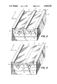
- FIG. 1 is a isometric side view, not to scale, of an embodiment of the invention.
- FIG. 2 is a view similar to FIG. 1 showing another embodiment of the invention.
- FIG. 3 is a view similar to FIG. 2 showing an advantageous variation of the device of FIG. 2.
- FIG. 4 is a graph showing the relationship between the drift velocity of carriers in n-doped gallium arsenide, as a function of field potential.
- an FET amplifier according to the invention is shown.
- the device has a unitary n-doped gallium arsenide layer with regions 2, 5, 6. Regions 5 and 6 are more heavily doped than region 2. Along with microstrip 1, region 5 constitutes the device's source; and along with microstrip 3, region 6 constitutes the device's drain. Region 2 of the unitary layer is the device's channel. Between microstrip 1 and 3 is un-doped superlattice 22 which has alternating sublayers of aluminum arsenide and gallium arsenide. Superlattice 22 acts as a heterojunction with channel 2 to reduce surface self-depletion in channel 2, thus increasing maximum channel current, and improving device output conductance.
- the unitary layer 2, 5, 6 of the device is preferably fabricated from semiconductor material such as gallium arsenide. Underlaying the device's channels is a layer 15 of aluminum arsenide heteroepitaxial with the layer of gallium arsenide 2, 5, 6. Underlaying layer 15 of aluminum arsenide is a semi-insulating substrate 10 of gallium arsenide having trench 16 to accommodate metallic gate 19. Beneath gate 19 is dielectric 14, and metal mounting substrate 18.
- gallium arsenide layer 10 Because the etchabilities of aluminum arsenide and gallium arsenide differ so greatly, the penetration of gallium arsenide layer 10 to the aluminum arsenide layer 15 in effect stops the etching process. Thus, one need not resort to exceptionally delicate techniques to control the depth of trench 16.
- the locally exposed surface of layer 15 is allowed to oxidize in air and a thin layer of gallium arsenide 24, is grown epitaxially on semi-insulating substrate 10 within trench 16.
- the epitaxially grown gallium arsenide (backfill) 24 does not grow on the oxidized aluminum arsenide surface, but does serve, by narrowing trench width, to shorten the effective distance (in the direction of electron propagation) of subsequently deposited metal control gate 19.
- the effective length of the control gate can be much less than would otherwise be possible from photolightography.
- Any polycrystalline GaAs deposited on the oxidized AlAs is easily differentially etched away. This narrowed gate length improves device performance (e.g., raises frequency range) without reducing device yield.
- the trench is filled with metal 19 to form the finished gate.
- placement of gate 19 on the opposite side of layer 15 from channel 2 provides for more efficient RF grounding of gate 19.
- a dielectric 14 is then placed thereunder, and final metal substrate 18 placed under dielectric 14.
- the geometry of the device is chosen so that the device's input portion (source 1, 5 and gate 11), and the device's output portion (drain 3, 6 and gate 19), are mirror images of one another.
- a traveling electromagnetic wave enters the device at the end of source strip 1 marked "IN”.
- the current in the device moves in the direction marked "y", i.e., through channel 2 between source 1, 5 and drain 3, 6 and serves to couple the signal from the device's input portion (source 1, 5 and gate 19) and output portion (drain 3, 6 and gate 19).
- the electromagnetic signal appears to move through the device in a vector direction between x and y.
- the stages are impedance and velocity matched, and the wave reinforces itself between the input and output portions, rather than cancels. Accordingly, this device can be made long in the "x" direction, the ultimate practical limitation on this dimension resulting from attenuation, rather than phase interference, with an increase in the device's power capacity corresponding to the device's increase in size.
- FIG. 2 a device is shown combining two such devices as shown in FIG. 1 into one integral two stage amplifier device.
- the unitary doped layer of gallium arsenide contains additional regions 8, which serves as the second stage's channel, and heavily doped region 7, which, along with microstrip 4, serves as the second stage's drain.
- Second stage gate 20 is disposed in gate trench 17 with epitaxial gallium arsenide growth 22 serving the same function as growth 24 of the first stage. Resistive portion 13 separating gates 19 and 20 sets the appropriate d.c. bias for the second state.
- microstrip 3 and region 6 also constitute the source of the device's second stage, the second stage's channel comprising heavily doped regions 6 and 7 and less heavily doped region 8. Because strip 3 and region 6 serve both amplifier stages, one has eliminated a part of the chip, as well as the manufacturing steps necessary to incorporate the part into the chip; thus the chip can be shortened, increasing device response time proportionately. Also, forming the plural stage device monolithically ensures great uniformity of material between corresponding mirror image points in each stage. This, along with device geometry, ensures that the phase velocities of signals propagating through different portions of the device will be virtually equal, virtually eliminating phase cancellation between stages, and between the input and output portions of each stage.
- FIG. 2 shows a device of two stages it is plain that a device of more than two such stages is equally within the scope of the invention.
- FIG. 3 a device very similar to that in FIG. 2, is illustrated with the important difference that the overlying metal strip (shown in FIG. 2 by reference numeral 3) is eliminated.
- region 6 of the device serves as the drain for the device's first stage, and source for the device's second stage. Because of the heavy impurity differential doping in region 6, it functions as a drain for region 2 and source for region 8. Thus, no external connection to this intermediate source-ground is necessary, and metalized strip 3 of FIG. 2 preferentially can be dispensed with, further simplifying the device, rendering it incrementally more reliable to fabricate, and eliminating reflections of electromagnetic signals at the ends, and unwanted backward traveling waves.
- region 2 do not interfere with the performance of the device.
- Region 6 forms not only a virtual drain for region 2 and a virtual source for region 8, but because of the low electric field within region 6 insures that electrons entering region 8 are in their low effective moss state characteristic of electron subjected to electric fields of less than 3.5 kV/cm as shown in FIG. 4.
Landscapes
- Junction Field-Effect Transistors (AREA)
Abstract
Description
Claims (7)
Priority Applications (1)
| Application Number | Priority Date | Filing Date | Title |
|---|---|---|---|
| US07/095,487 US4914743A (en) | 1987-08-27 | 1987-08-27 | Yoked orthogonally distributed equal reactance non-coplanar traveling wave amplifier |
Applications Claiming Priority (1)
| Application Number | Priority Date | Filing Date | Title |
|---|---|---|---|
| US07/095,487 US4914743A (en) | 1987-08-27 | 1987-08-27 | Yoked orthogonally distributed equal reactance non-coplanar traveling wave amplifier |
Publications (1)
| Publication Number | Publication Date |
|---|---|
| US4914743A true US4914743A (en) | 1990-04-03 |
Family
ID=22252239
Family Applications (1)
| Application Number | Title | Priority Date | Filing Date |
|---|---|---|---|
| US07/095,487 Expired - Fee Related US4914743A (en) | 1987-08-27 | 1987-08-27 | Yoked orthogonally distributed equal reactance non-coplanar traveling wave amplifier |
Country Status (1)
| Country | Link |
|---|---|
| US (1) | US4914743A (en) |
Cited By (5)
| Publication number | Priority date | Publication date | Assignee | Title |
|---|---|---|---|---|
| US5309007A (en) * | 1991-09-30 | 1994-05-03 | The United States Of America As Represented By The Secretary Of The Navy | Junction field effect transistor with lateral gate voltage swing (GVS-JFET) |
| US6090320A (en) * | 1996-12-04 | 2000-07-18 | Miba Sintermetall Aktiengesellschaft | Method of producing a sintered body |
| US20080099802A1 (en) * | 2006-10-24 | 2008-05-01 | Michael Vice | Transmission line transistor |
| US10224407B2 (en) | 2017-02-28 | 2019-03-05 | Sandisk Technologies Llc | High voltage field effect transistor with laterally extended gate dielectric and method of making thereof |
| US11075078B1 (en) * | 2020-03-06 | 2021-07-27 | Atomera Incorporated | Method for making a semiconductor device including a superlattice within a recessed etch |
Citations (2)
| Publication number | Priority date | Publication date | Assignee | Title |
|---|---|---|---|---|
| US4537654A (en) * | 1983-12-09 | 1985-08-27 | Trw Inc. | Two-gate non-coplanar FET with self-aligned source |
| US4755867A (en) * | 1986-08-15 | 1988-07-05 | American Telephone And Telegraph Company, At&T Bell Laboratories | Vertical Enhancement-mode Group III-V compound MISFETs |
-
1987
- 1987-08-27 US US07/095,487 patent/US4914743A/en not_active Expired - Fee Related
Patent Citations (2)
| Publication number | Priority date | Publication date | Assignee | Title |
|---|---|---|---|---|
| US4537654A (en) * | 1983-12-09 | 1985-08-27 | Trw Inc. | Two-gate non-coplanar FET with self-aligned source |
| US4755867A (en) * | 1986-08-15 | 1988-07-05 | American Telephone And Telegraph Company, At&T Bell Laboratories | Vertical Enhancement-mode Group III-V compound MISFETs |
Non-Patent Citations (4)
| Title |
|---|
| "Solicitation No. N00014-86-R-0047" (Source Selection Procedure: Traveling Wave Techniques for Broadband Power Amplifiers) (mailed on or about Sep. 1, 1986). |
| M. N. Yoder "Applications of Diamond Technology" (copies of viewgraphs sh Jul. 1986). |
| M. N. Yoder Applications of Diamond Technology (copies of viewgraphs shown Jul. 1986). * |
| Solicitation No. N00014 86 R 0047 (Source Selection Procedure: Traveling Wave Techniques for Broadband Power Amplifiers) (mailed on or about Sep. 1, 1986). * |
Cited By (6)
| Publication number | Priority date | Publication date | Assignee | Title |
|---|---|---|---|---|
| US5309007A (en) * | 1991-09-30 | 1994-05-03 | The United States Of America As Represented By The Secretary Of The Navy | Junction field effect transistor with lateral gate voltage swing (GVS-JFET) |
| US6090320A (en) * | 1996-12-04 | 2000-07-18 | Miba Sintermetall Aktiengesellschaft | Method of producing a sintered body |
| US20080099802A1 (en) * | 2006-10-24 | 2008-05-01 | Michael Vice | Transmission line transistor |
| GB2443719A (en) * | 2006-10-24 | 2008-05-14 | Avago Technologies Wireless Ip | Transmission line transistor |
| US10224407B2 (en) | 2017-02-28 | 2019-03-05 | Sandisk Technologies Llc | High voltage field effect transistor with laterally extended gate dielectric and method of making thereof |
| US11075078B1 (en) * | 2020-03-06 | 2021-07-27 | Atomera Incorporated | Method for making a semiconductor device including a superlattice within a recessed etch |
Similar Documents
| Publication | Publication Date | Title |
|---|---|---|
| EP3008760B1 (en) | Recessed field plate transistor structures | |
| US5473176A (en) | Vertical insulated gate transistor and method of manufacture | |
| JP5562925B2 (en) | Field effect transistor | |
| JP3499884B2 (en) | High power, high frequency metal-semiconductor field effect transistor | |
| EP0031366B1 (en) | Vertical field effect transistor | |
| US5091759A (en) | Heterostructure field effect transistor | |
| EP0514079B1 (en) | High electron mobility transistor and method of manufacture | |
| US4916498A (en) | High electron mobility power transistor | |
| US5196359A (en) | Method of forming heterostructure field effect transistor | |
| US6215136B1 (en) | Integrated circuit capable of low-noise and high-power microwave operation | |
| US10153273B1 (en) | Metal-semiconductor heterodimension field effect transistors (MESHFET) and high electron mobility transistor (HEMT) based device and method of making the same | |
| US5488237A (en) | Semiconductor device with delta-doped layer in channel region | |
| US5405797A (en) | Method of producing a monolithically integrated millimeter wave circuit | |
| US8809137B2 (en) | Leakage barrier for GaN based HEMT active device | |
| US5668387A (en) | Relaxed channel high electron mobility transistor | |
| US5324682A (en) | Method of making an integrated circuit capable of low-noise and high-power microwave operation | |
| EP0015072A1 (en) | A field effect transistor | |
| US4914743A (en) | Yoked orthogonally distributed equal reactance non-coplanar traveling wave amplifier | |
| US5834802A (en) | Metal semiconductor field effect transistors having improved intermodulation distortion using different pinch-off voltages | |
| US5252842A (en) | Low-loss semiconductor device and backside etching method for manufacturing same | |
| WO2022101736A1 (en) | Multi-threshold voltage gallium nitride high electron mobility transistor | |
| KR960000385B1 (en) | Field Effect Transistor | |
| US4590502A (en) | Camel gate field effect transistor device | |
| KR0174879B1 (en) | Isolation of Compound Semiconductor Devices | |
| KR100312368B1 (en) | Compound semiconductor integrated circuit and optical regenerator using the same |
Legal Events
| Date | Code | Title | Description |
|---|---|---|---|
| AS | Assignment |
Owner name: UNITED STATES OF AMERICA, THE, AS REPRESENTED BY T Free format text: ASSIGNMENT OF ASSIGNORS INTEREST.;ASSIGNOR:YODER, MAX N.;REEL/FRAME:004799/0103 Effective date: 19871103 Owner name: UNITED STATES OF AMERICA, THE, AS REPRESENTED BY T Free format text: ASSIGNMENT OF ASSIGNORS INTEREST.;ASSIGNOR:MORGAN, MICHAEL A.;REEL/FRAME:004799/0104 Effective date: 19871116 Owner name: UNITED STATES OF AMERICA, THE, AS REPRESENTED BY T Free format text: ASSIGNMENT OF ASSIGNORS INTEREST;ASSIGNOR:YODER, MAX N.;REEL/FRAME:004799/0103 Effective date: 19871103 Owner name: UNITED STATES OF AMERICA, THE, AS REPRESENTED BY T Free format text: ASSIGNMENT OF ASSIGNORS INTEREST;ASSIGNOR:MORGAN, MICHAEL A.;REEL/FRAME:004799/0104 Effective date: 19871116 |
|
| FPAY | Fee payment |
Year of fee payment: 4 |
|
| REMI | Maintenance fee reminder mailed | ||
| LAPS | Lapse for failure to pay maintenance fees | ||
| FP | Lapsed due to failure to pay maintenance fee |
Effective date: 19980408 |
|
| STCH | Information on status: patent discontinuation |
Free format text: PATENT EXPIRED DUE TO NONPAYMENT OF MAINTENANCE FEES UNDER 37 CFR 1.362 |