US4900518A - Gaseous organic/inorganic thermal cracker for vacuum chemical epitaxy - Google Patents
Gaseous organic/inorganic thermal cracker for vacuum chemical epitaxy Download PDFInfo
- Publication number
- US4900518A US4900518A US07/279,273 US27927388A US4900518A US 4900518 A US4900518 A US 4900518A US 27927388 A US27927388 A US 27927388A US 4900518 A US4900518 A US 4900518A
- Authority
- US
- United States
- Prior art keywords
- tube
- heating
- graphite
- heat shield
- surrounding
- Prior art date
- Legal status (The legal status is an assumption and is not a legal conclusion. Google has not performed a legal analysis and makes no representation as to the accuracy of the status listed.)
- Expired - Lifetime
Links
- 238000000407 epitaxy Methods 0.000 title description 2
- 239000000126 substance Substances 0.000 title description 2
- 239000007789 gas Substances 0.000 claims abstract description 27
- 229910001872 inorganic gas Inorganic materials 0.000 claims abstract description 5
- 238000010438 heat treatment Methods 0.000 claims description 20
- OKTJSMMVPCPJKN-UHFFFAOYSA-N Carbon Chemical compound [C] OKTJSMMVPCPJKN-UHFFFAOYSA-N 0.000 claims description 13
- 229910002804 graphite Inorganic materials 0.000 claims description 13
- 239000010439 graphite Substances 0.000 claims description 13
- 229910052715 tantalum Inorganic materials 0.000 claims description 6
- GUVRBAGPIYLISA-UHFFFAOYSA-N tantalum atom Chemical compound [Ta] GUVRBAGPIYLISA-UHFFFAOYSA-N 0.000 claims description 6
- 229910018404 Al2 O3 Inorganic materials 0.000 claims description 2
- DECCZIUVGMLHKQ-UHFFFAOYSA-N rhenium tungsten Chemical compound [W].[Re] DECCZIUVGMLHKQ-UHFFFAOYSA-N 0.000 claims description 2
- XYFCBTPGUUZFHI-UHFFFAOYSA-N Phosphine Chemical compound P XYFCBTPGUUZFHI-UHFFFAOYSA-N 0.000 abstract description 10
- RBFQJDQYXXHULB-UHFFFAOYSA-N arsane Chemical compound [AsH3] RBFQJDQYXXHULB-UHFFFAOYSA-N 0.000 abstract description 10
- 238000005336 cracking Methods 0.000 abstract description 9
- 239000004065 semiconductor Substances 0.000 abstract description 9
- 150000001875 compounds Chemical class 0.000 abstract description 8
- 229910000073 phosphorus hydride Inorganic materials 0.000 abstract description 5
- 238000004227 thermal cracking Methods 0.000 abstract description 5
- 239000000356 contaminant Substances 0.000 abstract 1
- 238000000034 method Methods 0.000 description 10
- 229910052785 arsenic Inorganic materials 0.000 description 7
- RQNWIZPPADIBDY-UHFFFAOYSA-N arsenic atom Chemical compound [As] RQNWIZPPADIBDY-UHFFFAOYSA-N 0.000 description 7
- 239000000463 material Substances 0.000 description 7
- BHEPBYXIRTUNPN-UHFFFAOYSA-N hydridophosphorus(.) (triplet) Chemical compound [PH] BHEPBYXIRTUNPN-UHFFFAOYSA-N 0.000 description 4
- 239000012535 impurity Substances 0.000 description 4
- 238000001451 molecular beam epitaxy Methods 0.000 description 4
- 238000005229 chemical vapour deposition Methods 0.000 description 3
- 239000012212 insulator Substances 0.000 description 3
- 238000004519 manufacturing process Methods 0.000 description 3
- 239000010453 quartz Substances 0.000 description 3
- VYPSYNLAJGMNEJ-UHFFFAOYSA-N silicon dioxide Inorganic materials O=[Si]=O VYPSYNLAJGMNEJ-UHFFFAOYSA-N 0.000 description 3
- JBRZTFJDHDCESZ-UHFFFAOYSA-N AsGa Chemical compound [As]#[Ga] JBRZTFJDHDCESZ-UHFFFAOYSA-N 0.000 description 2
- 229910001218 Gallium arsenide Inorganic materials 0.000 description 2
- 229910000070 arsenic hydride Inorganic materials 0.000 description 2
- 238000011109 contamination Methods 0.000 description 2
- 230000002939 deleterious effect Effects 0.000 description 2
- -1 i.e. Chemical compound 0.000 description 2
- 150000002894 organic compounds Chemical class 0.000 description 2
- WFKWXMTUELFFGS-UHFFFAOYSA-N tungsten Chemical compound [W] WFKWXMTUELFFGS-UHFFFAOYSA-N 0.000 description 2
- 229910052721 tungsten Inorganic materials 0.000 description 2
- 239000010937 tungsten Substances 0.000 description 2
- 229910005540 GaP Inorganic materials 0.000 description 1
- GYHNNYVSQQEPJS-UHFFFAOYSA-N Gallium Chemical compound [Ga] GYHNNYVSQQEPJS-UHFFFAOYSA-N 0.000 description 1
- UFHFLCQGNIYNRP-UHFFFAOYSA-N Hydrogen Chemical compound [H][H] UFHFLCQGNIYNRP-UHFFFAOYSA-N 0.000 description 1
- XUIMIQQOPSSXEZ-UHFFFAOYSA-N Silicon Chemical compound [Si] XUIMIQQOPSSXEZ-UHFFFAOYSA-N 0.000 description 1
- 238000010521 absorption reaction Methods 0.000 description 1
- 239000006227 byproduct Substances 0.000 description 1
- 230000015556 catabolic process Effects 0.000 description 1
- 230000003197 catalytic effect Effects 0.000 description 1
- 238000006243 chemical reaction Methods 0.000 description 1
- 230000007547 defect Effects 0.000 description 1
- 238000005516 engineering process Methods 0.000 description 1
- 230000006870 function Effects 0.000 description 1
- 229910052733 gallium Inorganic materials 0.000 description 1
- HZXMRANICFIONG-UHFFFAOYSA-N gallium phosphide Chemical compound [Ga]#P HZXMRANICFIONG-UHFFFAOYSA-N 0.000 description 1
- 239000001257 hydrogen Substances 0.000 description 1
- 229910052739 hydrogen Inorganic materials 0.000 description 1
- 238000010348 incorporation Methods 0.000 description 1
- 150000002484 inorganic compounds Chemical class 0.000 description 1
- 229910010272 inorganic material Inorganic materials 0.000 description 1
- 238000012986 modification Methods 0.000 description 1
- 230000004048 modification Effects 0.000 description 1
- 238000012544 monitoring process Methods 0.000 description 1
- 125000004430 oxygen atom Chemical group O* 0.000 description 1
- 229920000642 polymer Polymers 0.000 description 1
- 229910052710 silicon Inorganic materials 0.000 description 1
- 239000010703 silicon Substances 0.000 description 1
- 229910001220 stainless steel Inorganic materials 0.000 description 1
- 239000010935 stainless steel Substances 0.000 description 1
- 239000000758 substrate Substances 0.000 description 1
- 231100000331 toxic Toxicity 0.000 description 1
- 230000002588 toxic effect Effects 0.000 description 1
- RGGPNXQUMRMPRA-UHFFFAOYSA-N triethylgallium Chemical compound CC[Ga](CC)CC RGGPNXQUMRMPRA-UHFFFAOYSA-N 0.000 description 1
- 238000004804 winding Methods 0.000 description 1
Images
Classifications
-
- C—CHEMISTRY; METALLURGY
- C30—CRYSTAL GROWTH
- C30B—SINGLE-CRYSTAL GROWTH; UNIDIRECTIONAL SOLIDIFICATION OF EUTECTIC MATERIAL OR UNIDIRECTIONAL DEMIXING OF EUTECTOID MATERIAL; REFINING BY ZONE-MELTING OF MATERIAL; PRODUCTION OF A HOMOGENEOUS POLYCRYSTALLINE MATERIAL WITH DEFINED STRUCTURE; SINGLE CRYSTALS OR HOMOGENEOUS POLYCRYSTALLINE MATERIAL WITH DEFINED STRUCTURE; AFTER-TREATMENT OF SINGLE CRYSTALS OR A HOMOGENEOUS POLYCRYSTALLINE MATERIAL WITH DEFINED STRUCTURE; APPARATUS THEREFOR
- C30B25/00—Single-crystal growth by chemical reaction of reactive gases, e.g. chemical vapour-deposition growth
- C30B25/02—Epitaxial-layer growth
-
- C—CHEMISTRY; METALLURGY
- C23—COATING METALLIC MATERIAL; COATING MATERIAL WITH METALLIC MATERIAL; CHEMICAL SURFACE TREATMENT; DIFFUSION TREATMENT OF METALLIC MATERIAL; COATING BY VACUUM EVAPORATION, BY SPUTTERING, BY ION IMPLANTATION OR BY CHEMICAL VAPOUR DEPOSITION, IN GENERAL; INHIBITING CORROSION OF METALLIC MATERIAL OR INCRUSTATION IN GENERAL
- C23C—COATING METALLIC MATERIAL; COATING MATERIAL WITH METALLIC MATERIAL; SURFACE TREATMENT OF METALLIC MATERIAL BY DIFFUSION INTO THE SURFACE, BY CHEMICAL CONVERSION OR SUBSTITUTION; COATING BY VACUUM EVAPORATION, BY SPUTTERING, BY ION IMPLANTATION OR BY CHEMICAL VAPOUR DEPOSITION, IN GENERAL
- C23C16/00—Chemical coating by decomposition of gaseous compounds, without leaving reaction products of surface material in the coating, i.e. chemical vapour deposition [CVD] processes
- C23C16/22—Chemical coating by decomposition of gaseous compounds, without leaving reaction products of surface material in the coating, i.e. chemical vapour deposition [CVD] processes characterised by the deposition of inorganic material, other than metallic material
- C23C16/30—Deposition of compounds, mixtures or solid solutions, e.g. borides, carbides, nitrides
- C23C16/301—AIII BV compounds, where A is Al, Ga, In or Tl and B is N, P, As, Sb or Bi
-
- C—CHEMISTRY; METALLURGY
- C23—COATING METALLIC MATERIAL; COATING MATERIAL WITH METALLIC MATERIAL; CHEMICAL SURFACE TREATMENT; DIFFUSION TREATMENT OF METALLIC MATERIAL; COATING BY VACUUM EVAPORATION, BY SPUTTERING, BY ION IMPLANTATION OR BY CHEMICAL VAPOUR DEPOSITION, IN GENERAL; INHIBITING CORROSION OF METALLIC MATERIAL OR INCRUSTATION IN GENERAL
- C23C—COATING METALLIC MATERIAL; COATING MATERIAL WITH METALLIC MATERIAL; SURFACE TREATMENT OF METALLIC MATERIAL BY DIFFUSION INTO THE SURFACE, BY CHEMICAL CONVERSION OR SUBSTITUTION; COATING BY VACUUM EVAPORATION, BY SPUTTERING, BY ION IMPLANTATION OR BY CHEMICAL VAPOUR DEPOSITION, IN GENERAL
- C23C16/00—Chemical coating by decomposition of gaseous compounds, without leaving reaction products of surface material in the coating, i.e. chemical vapour deposition [CVD] processes
- C23C16/44—Chemical coating by decomposition of gaseous compounds, without leaving reaction products of surface material in the coating, i.e. chemical vapour deposition [CVD] processes characterised by the method of coating
- C23C16/448—Chemical coating by decomposition of gaseous compounds, without leaving reaction products of surface material in the coating, i.e. chemical vapour deposition [CVD] processes characterised by the method of coating characterised by the method used for generating reactive gas streams, e.g. by evaporation or sublimation of precursor materials
- C23C16/452—Chemical coating by decomposition of gaseous compounds, without leaving reaction products of surface material in the coating, i.e. chemical vapour deposition [CVD] processes characterised by the method of coating characterised by the method used for generating reactive gas streams, e.g. by evaporation or sublimation of precursor materials by activating reactive gas streams before their introduction into the reaction chamber, e.g. by ionisation or addition of reactive species
-
- C—CHEMISTRY; METALLURGY
- C30—CRYSTAL GROWTH
- C30B—SINGLE-CRYSTAL GROWTH; UNIDIRECTIONAL SOLIDIFICATION OF EUTECTIC MATERIAL OR UNIDIRECTIONAL DEMIXING OF EUTECTOID MATERIAL; REFINING BY ZONE-MELTING OF MATERIAL; PRODUCTION OF A HOMOGENEOUS POLYCRYSTALLINE MATERIAL WITH DEFINED STRUCTURE; SINGLE CRYSTALS OR HOMOGENEOUS POLYCRYSTALLINE MATERIAL WITH DEFINED STRUCTURE; AFTER-TREATMENT OF SINGLE CRYSTALS OR A HOMOGENEOUS POLYCRYSTALLINE MATERIAL WITH DEFINED STRUCTURE; APPARATUS THEREFOR
- C30B29/00—Single crystals or homogeneous polycrystalline material with defined structure characterised by the material or by their shape
- C30B29/10—Inorganic compounds or compositions
- C30B29/40—AIIIBV compounds wherein A is B, Al, Ga, In or Tl and B is N, P, As, Sb or Bi
Definitions
- This invention relates to an apparatus capable of disassociating gaseous compounds. More specifically, this invention relates to a thermal cracking apparatus capable of disassociating organic or inorganic gaseous compounds and particularly to an apparatus capable of disassociating organic or inorganic compounds in the gaseous state by vacuum chemical epitaxy, (VCE).
- VCE vacuum chemical epitaxy
- III-V compound semiconductor layers require the use of arsenic and phosphorous in, for example, gallium arsenide, gallium phosphide, gallium arsenide phosphide, and the like.
- MBE molecular beam epitaxy
- elemental arsenic and phosphorous are often heated to obtain the species necessary to grow the desired semiconductor layers.
- the species of arsenic, i.e., As 4 derived from heating elemental arsenic or phosphorous are difficult to handle and the polymer from leads to point defects or regions of high phosphorous or arsenic concentrations in the growing layer.
- phosphine, Ph 3 , and arsine, AsH 3 have been used in chemical vapor deposition, (CVD), and MBE growth processes. These materials are generally broken down into smaller molecules or components by heating the molecule above its bond breaking temperature, i.e., "cracked” into useful species of P 2 and As 2 by passing them through a heated zone to liberated the hydrogen as H 2 gas.
- the process of using the gas in a heated atmosphere to break down the arsine and phosphine is generally referred to as thermal cracking.
- Thermal crackers in the past have involved a tube through which the gas is passed coming into direct contact with a heating wire such as a material made from tungsten and tantalum. Although these devices are capable of cracking the gases, the process of subjecting the gases to direct contact with the heater wire permits the incorporation of impurities in the gas, both tantalum or tungsten and other impurities during the process of heating the filament to a temperature sufficiently high to crack the gas. In addition, the heating filament lifetime is shortened by coming into direct contact with the gas or gases during the heating operation.
- VCE is a highly promising growth technique for meeting the economic needs for the high volume production of III-V compound semiconductor devices.
- the technique involves, among other things, the controllability of MBE with the ease of scaling of CVD while minimizing the amounts of toxic gaseous by-products and high temperature handling problems.
- an apparatus which is capable of thermally cracking phosphine, arsine, or organic compounds such as trimethyl or triethyl gallium.
- the apparatus can thermally crack organic and inorganic gases and provide the necessary semiconductor species for epitaxal layer growth without bringing the gases into direct contact with the heating filament.
- the invention also provides for the capability of thermally monitoring the cracking temperature to adjust the rate of cracking.
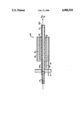
- the drawing illustrates a cross-sectional view of an embodiment of a thermal cracker according to our invention.
- FIGURE illustrates an organic/inorganic thermal cracker 100.
- Thermal cracker 100 includes a central elongate tube 10 of graphite or other suitable material which is stable at cracking temperatures and does not add deleterious impurities to the cracked gas stream.
- Prior art heaters have used quartz tubes which disassociate at thermal cracking temperatures to inject silicon and oxygen atom impurities into the gaseous stream during the semiconductor layer-fabrication.
- Graphite is stable in a reducing environment.
- the tube 10 is connected to a vacuum seal and flange 12 which fits into the wall of the vacuum chamber, the tube 10 connects to the outside of the chamber through a suitable gas-carrying tube 14 such as a stainless steel tube or a graphite tube. Tube 14 connects to the arsine or phosphine gaseous sources.
- a heating coil 16 of tungsten-rhenium or other suitable heating wires Surrounding the graphite tube is a heating coil 16 of tungsten-rhenium or other suitable heating wires.
- the heating-coil wire 16 is sandwiched between insulating tubes 20 and 22.
- Suitable insulating tubes can be fabricated from Al 2 O 3 or like materials which are stable at the temperatures necessary to crack the gas and will not introduce any deleterious gaseous or ionic species into the vacuum chamber atmosphere.
- the length of the heating coil 16 and the number of windings is a function of the amount of gas to be cracked and the rapidity with which the gas needs to be cracked.
- the heating coil should be as short as possible to minimize the amount of heat injected into the vacuum chamber portion of the VCE apparatus.
- the heating wire 16 is connected to the outside through a suitable vacuum seal 12 via wire 16a.
- a heat shield 24 surrounds the outer insulator tube 22.
- the heat shield 24 is fabricated from tantalum or any other suitable material capable of protecting the insulator tubes while maximizing the inward temperature profile and minimizing the amount of heat radiated to the surrounding vacuum chamber.
- thermocouple 18 sandwiched between the tantalum heat shield and the outer insulator tube 22.
- the thermocouple is connected to the outside environment by a feed-through in vacuum flange 12.
- the thermocouple can be embedded within the graphite tube 10 as close to the interior of the tube as possible.
- the apparatus 100 is screwed into the wall of the vacuum chamber, the vacuum is reduced to the range of 10 -5 Torr or better, and preferably, between 10 -7 Torr to 10 -8 Torr while energizing the heater coil and introducing an inorganic gas such as arsine 300 through tube 14 into graphite tube 10.
- the flow rate of the arsine 300 is adjusted to achieve the desired amount of cracked arsenic as As 2 and H 2 gases 400 exiting the graphite tube to react with the III compound materials of gallium and the like, at the substrate surface to form the required III-V compound semiconductor layers
- the thermal cracker of our invention provides a straight-forward cracker apparatus and process of cracking gases without the requirement of catalytic wires or baffles or quartz surfaces which can contaminate the cracked gases.
Landscapes
- Chemical & Material Sciences (AREA)
- Engineering & Computer Science (AREA)
- Materials Engineering (AREA)
- Metallurgy (AREA)
- Organic Chemistry (AREA)
- General Chemical & Material Sciences (AREA)
- Chemical Kinetics & Catalysis (AREA)
- Inorganic Chemistry (AREA)
- Mechanical Engineering (AREA)
- Crystallography & Structural Chemistry (AREA)
- Crystals, And After-Treatments Of Crystals (AREA)
Abstract
Description
Claims (6)
Priority Applications (1)
| Application Number | Priority Date | Filing Date | Title |
|---|---|---|---|
| US07/279,273 US4900518A (en) | 1986-12-12 | 1988-12-02 | Gaseous organic/inorganic thermal cracker for vacuum chemical epitaxy |
Applications Claiming Priority (2)
| Application Number | Priority Date | Filing Date | Title |
|---|---|---|---|
| US94100386A | 1986-12-12 | 1986-12-12 | |
| US07/279,273 US4900518A (en) | 1986-12-12 | 1988-12-02 | Gaseous organic/inorganic thermal cracker for vacuum chemical epitaxy |
Related Parent Applications (1)
| Application Number | Title | Priority Date | Filing Date |
|---|---|---|---|
| US94100386A Continuation | 1986-12-12 | 1986-12-12 |
Publications (1)
| Publication Number | Publication Date |
|---|---|
| US4900518A true US4900518A (en) | 1990-02-13 |
Family
ID=26959559
Family Applications (1)
| Application Number | Title | Priority Date | Filing Date |
|---|---|---|---|
| US07/279,273 Expired - Lifetime US4900518A (en) | 1986-12-12 | 1988-12-02 | Gaseous organic/inorganic thermal cracker for vacuum chemical epitaxy |
Country Status (1)
| Country | Link |
|---|---|
| US (1) | US4900518A (en) |
Cited By (3)
| Publication number | Priority date | Publication date | Assignee | Title |
|---|---|---|---|---|
| US4983234A (en) * | 1987-11-12 | 1991-01-08 | The Secretary Of State For Defence In Her Britannic Majesty's Government Of The United Kingdom Of Great Britain And Northern Ireland | Phosphine inhibition |
| US5354412A (en) * | 1991-09-13 | 1994-10-11 | Nippondenso Co., Ltd. | Method of making a compound semiconductor device |
| US20050026965A1 (en) * | 2000-12-29 | 2005-02-03 | Darwin Discovery Limited | Pharmaceutical uses and synthesis of nicotinanilide-N-oxides |
Citations (6)
| Publication number | Priority date | Publication date | Assignee | Title |
|---|---|---|---|---|
| US699146A (en) * | 1902-03-03 | 1902-05-06 | Shickle Harrison And Howard Iron Company | Electric combustion-furnace. |
| US3541293A (en) * | 1968-10-29 | 1970-11-17 | Ronald Macdonald | Muffle furnace |
| US3804967A (en) * | 1972-10-13 | 1974-04-16 | Sola Basic Ind Inc | Rectangular tube diffusion furnace |
| US4397431A (en) * | 1981-11-02 | 1983-08-09 | Avco Corporation | Fail-safe, anti-icing system for aircraft engines |
| US4518846A (en) * | 1984-06-11 | 1985-05-21 | International Business Machines Corporation | Heater assembly for molecular beam epitaxy furnace |
| US4544025A (en) * | 1984-01-17 | 1985-10-01 | The United States Of America As Represented By The Administrator Of The National Aeronautics And Space Administration | High gradient directional solidification furnace |
-
1988
- 1988-12-02 US US07/279,273 patent/US4900518A/en not_active Expired - Lifetime
Patent Citations (6)
| Publication number | Priority date | Publication date | Assignee | Title |
|---|---|---|---|---|
| US699146A (en) * | 1902-03-03 | 1902-05-06 | Shickle Harrison And Howard Iron Company | Electric combustion-furnace. |
| US3541293A (en) * | 1968-10-29 | 1970-11-17 | Ronald Macdonald | Muffle furnace |
| US3804967A (en) * | 1972-10-13 | 1974-04-16 | Sola Basic Ind Inc | Rectangular tube diffusion furnace |
| US4397431A (en) * | 1981-11-02 | 1983-08-09 | Avco Corporation | Fail-safe, anti-icing system for aircraft engines |
| US4544025A (en) * | 1984-01-17 | 1985-10-01 | The United States Of America As Represented By The Administrator Of The National Aeronautics And Space Administration | High gradient directional solidification furnace |
| US4518846A (en) * | 1984-06-11 | 1985-05-21 | International Business Machines Corporation | Heater assembly for molecular beam epitaxy furnace |
Non-Patent Citations (21)
| Title |
|---|
| A. R. Calawa, "On the Use of AsH3 in the Molecular Beam Epitaxial Growth of GaAs," Appl. Phys. Lett. 38 (9), 1 May 1981, pp. 701-703. |
| A. R. Calawa, On the Use of AsH 3 in the Molecular Beam Epitaxial Growth of GaAs, Appl. Phys. Lett. 38 (9), 1 May 1981, pp. 701 703. * |
| Ando et al., "Metalorganic Molecular Beam Opitaxial Growth of AnSe Using . . ." Jap. Jorn. of Appl., vol. 25, No. 4, Apr. 1986, pp. L279-L281. |
| Ando et al., Metalorganic Molecular Beam Opitaxial Growth of AnSe Using . . . Jap. Jorn. of Appl., vol. 25, No. 4, Apr. 1986, pp. L279 L281. * |
| Huet et al., "Molecular Beam Epitaxy of In0.53 GA0.47 As and InP by Using Cracker . . ." J. Vac. Sci. Technol B3(3), May/Jun. 1985, pp. 823-829. |
| Huet et al., Molecular Beam Epitaxy of In 0.53 GA 0.47 As and InP by Using Cracker . . . J. Vac. Sci. Technol B3(3), May/Jun. 1985, pp. 823 829. * |
| Kapitan et al., "On the Design and Characterization of a Novel Arsine Cracking . . ." J. Vac. Sci. Technol B2(2), Apr.-Jun. 1984, pp. 280-284. |
| Kapitan et al., On the Design and Characterization of a Novel Arsine Cracking . . . J. Vac. Sci. Technol B2(2), Apr. Jun. 1984, pp. 280 284. * |
| L. D. Portain et al., "Vacuum MOCVD Fabrication of High Efficiency Cells for Multi-Junction Application," Space Photovoltaic Research & Tech. Conference, Apr. 30-May 2, 1985, pp. 1-9. |
| L. D. Portain et al., Vacuum MOCVD Fabrication of High Efficiency Cells for Multi Junction Application, Space Photovoltaic Research & Tech. Conference, Apr. 30 May 2, 1985, pp. 1 9. * |
| L. M. Fraas et al., "Vacuum Chemical Epitaxy Utilizing Organomablic Sources", J. Elec. Materials, vol. 15, No. 3, pp. 175"180, May 1986. |
| L. M. Fraas et al., Vacuum Chemical Epitaxy Utilizing Organomablic Sources , J. Elec. Materials, vol. 15, No. 3, pp. 175 180, May 1986. * |
| Lee et al., "Material Effects on the Cracking Efficiency of Molecular Beam . . ." J. Vac. Sci. Technol. B4(2), Mar./Apr. 1986, pp. 568-570. |
| Lee et al., Material Effects on the Cracking Efficiency of Molecular Beam . . . J. Vac. Sci. Technol. B4(2), Mar./Apr. 1986, pp. 568 570. * |
| Panish et al., "Gas Source MBE of InP and Gax In1 -x Py As1 -y: Materials Properties . . ." J. Vac. Sci. Technol. B3(2), Mar./Apr. 1985, pp. 657"665. |
| Panish et al., Gas Source MBE of InP and Ga x In 1 x P y As 1 y: Materials Properties . . . J. Vac. Sci. Technol. B3(2), Mar./Apr. 1985, pp. 657 665. * |
| R. Chow et al., "Electrical and Optical Properties of InP Grown by Molecular Beam Epitaxy . . ." Appl. Phys. Letter 42(4), 15 Feb. 1983, pp. 383-385. |
| R. Chow et al., Electrical and Optical Properties of InP Grown by Molecular Beam Epitaxy . . . Appl. Phys. Letter 42(4), 15 Feb. 1983, pp. 383 385. * |
| Research on Multiband Gap Solar Cells, SERI Semiannual Control Report, Mar. 31, 1985 to Aug. 31, 1985 submitted on or about Oct. 16, 1986 for initial approval and mailed to listed recipents on or about Dec. 16, 1985. * |
| SERI Contract Monthly Report Apr. 1 30, 1985, Submitted May 15, 1985. * |
| SERI Contract Monthly Report Apr. 1-30, 1985, Submitted May 15, 1985. |
Cited By (3)
| Publication number | Priority date | Publication date | Assignee | Title |
|---|---|---|---|---|
| US4983234A (en) * | 1987-11-12 | 1991-01-08 | The Secretary Of State For Defence In Her Britannic Majesty's Government Of The United Kingdom Of Great Britain And Northern Ireland | Phosphine inhibition |
| US5354412A (en) * | 1991-09-13 | 1994-10-11 | Nippondenso Co., Ltd. | Method of making a compound semiconductor device |
| US20050026965A1 (en) * | 2000-12-29 | 2005-02-03 | Darwin Discovery Limited | Pharmaceutical uses and synthesis of nicotinanilide-N-oxides |
Similar Documents
| Publication | Publication Date | Title |
|---|---|---|
| KR850001943B1 (en) | Combination gas curtains for continuous chemical vapor deposition production of silicon bodies | |
| US6056820A (en) | Advanced physical vapor transport method and apparatus for growing high purity single crystal silicon carbide | |
| US5246500A (en) | Vapor phase epitaxial growth apparatus | |
| EP0259777B1 (en) | Method for growing single crystal thin films of element semiconductor | |
| US4920918A (en) | Pressure-resistant thermal reactor system for semiconductor processing | |
| US5194401A (en) | Thermally processing semiconductor wafers at non-ambient pressures | |
| US9039411B2 (en) | Thermal treatment apparatus | |
| KR850001944B1 (en) | Continuous production method of crystalline silicon | |
| US5225378A (en) | Method of forming a phosphorus doped silicon film | |
| JP2505777B2 (en) | Epitaxial layer deposition method for semiconductor materials | |
| KR850001942B1 (en) | Gas curtain continuous chemical vapor deposition production of semiconductor bodies | |
| US20040178176A1 (en) | Apparatus and method for cleaning a bell jar in a barrel epitaxial reactor | |
| KR910005380A (en) | Chemical vapor growth apparatus and method | |
| US4900518A (en) | Gaseous organic/inorganic thermal cracker for vacuum chemical epitaxy | |
| CN1397985A (en) | Mfg. method of lining processor and semiconductor device | |
| US5881090A (en) | Quartz used in semiconductor manufacturing device, apparatus for manufacturing the quartz, and method for manufacturing the same | |
| US4873119A (en) | Catalytic deposition of semiconductors | |
| US3340848A (en) | Apparatus for producing purs semiconductor material | |
| JPH10149986A (en) | Method and device for manufacturing diamond n-type semiconductor film | |
| JPH01123411A (en) | Vapor phase growth method and apparatus | |
| Boldish et al. | The quartz-envelope heater: A new heater for metal-organic chemical vapor deposition systems | |
| JPH07176498A (en) | Reactor with reaction gas preheater | |
| JP2714824B2 (en) | Molecular beam epitaxial growth method and apparatus for implementing the method | |
| JPS63181414A (en) | Apparatus for forming semiconductor film | |
| JPH0582040U (en) | Semiconductor heat treatment equipment |
Legal Events
| Date | Code | Title | Description |
|---|---|---|---|
| STCF | Information on status: patent grant |
Free format text: PATENTED CASE |
|
| CC | Certificate of correction | ||
| FPAY | Fee payment |
Year of fee payment: 4 |
|
| FPAY | Fee payment |
Year of fee payment: 8 |
|
| FEPP | Fee payment procedure |
Free format text: PAYOR NUMBER ASSIGNED (ORIGINAL EVENT CODE: ASPN); ENTITY STATUS OF PATENT OWNER: LARGE ENTITY |
|
| AS | Assignment |
Owner name: DAIDO HOXAN, INC., JAPAN Free format text: MERGER;ASSIGNOR:DAIDOUSANSO CO., LTD.;REEL/FRAME:011356/0773 Effective date: 19930630 |
|
| AS | Assignment |
Owner name: AIR WATER, INC., JAPAN Free format text: CHANGE OF NAME;ASSIGNOR:DAIDO HOXAN INC.;REEL/FRAME:011356/0785 Effective date: 20000403 |
|
| FPAY | Fee payment |
Year of fee payment: 12 |