US4900283A - Method for arranging chips each having an array of semiconductor light emitting elements - Google Patents
Method for arranging chips each having an array of semiconductor light emitting elements Download PDFInfo
- Publication number
- US4900283A US4900283A US07/079,678 US7967887A US4900283A US 4900283 A US4900283 A US 4900283A US 7967887 A US7967887 A US 7967887A US 4900283 A US4900283 A US 4900283A
- Authority
- US
- United States
- Prior art keywords
- chips
- light emitting
- semiconductor light
- leds
- cutting
- Prior art date
- Legal status (The legal status is an assumption and is not a legal conclusion. Google has not performed a legal analysis and makes no representation as to the accuracy of the status listed.)
- Expired - Lifetime
Links
Images
Classifications
-
- B—PERFORMING OPERATIONS; TRANSPORTING
- B41—PRINTING; LINING MACHINES; TYPEWRITERS; STAMPS
- B41J—TYPEWRITERS; SELECTIVE PRINTING MECHANISMS, i.e. MECHANISMS PRINTING OTHERWISE THAN FROM A FORME; CORRECTION OF TYPOGRAPHICAL ERRORS
- B41J2/00—Typewriters or selective printing mechanisms characterised by the printing or marking process for which they are designed
- B41J2/435—Typewriters or selective printing mechanisms characterised by the printing or marking process for which they are designed characterised by selective application of radiation to a printing material or impression-transfer material
- B41J2/447—Typewriters or selective printing mechanisms characterised by the printing or marking process for which they are designed characterised by selective application of radiation to a printing material or impression-transfer material using arrays of radiation sources
- B41J2/45—Typewriters or selective printing mechanisms characterised by the printing or marking process for which they are designed characterised by selective application of radiation to a printing material or impression-transfer material using arrays of radiation sources using light-emitting diode [LED] or laser arrays
-
- Y—GENERAL TAGGING OF NEW TECHNOLOGICAL DEVELOPMENTS; GENERAL TAGGING OF CROSS-SECTIONAL TECHNOLOGIES SPANNING OVER SEVERAL SECTIONS OF THE IPC; TECHNICAL SUBJECTS COVERED BY FORMER USPC CROSS-REFERENCE ART COLLECTIONS [XRACs] AND DIGESTS
- Y10—TECHNICAL SUBJECTS COVERED BY FORMER USPC
- Y10T—TECHNICAL SUBJECTS COVERED BY FORMER US CLASSIFICATION
- Y10T29/00—Metal working
- Y10T29/49—Method of mechanical manufacture
- Y10T29/49826—Assembling or joining
- Y10T29/49904—Assembling a subassembly, then assembling with a second subassembly
Definitions
- This invention relates to semiconductor devices and more particularly to such devices operable to emit light.
- LEDs Light emitting diodes
- Such devices are used to form an array of devices or elements each of which produces a light output (or not) depending upon whether it is activated or not. It is known to use a linear array of LED elements to expose consecutive linear segments of an electrostatic drum commonly used in photocopiers. The LEDs discharge the consecutive linear segments of the drum as the drum rotates.
- LEDs may be arranged in groups where each group is aligned along an axis at 45° with respect to the direction of rotation of the drum. The end diodes of each group are aligned adjacent to a line parallel to the direction of rotation. Again, when properly activated, the effect of a straight linear array across the entire drum is achieved.
- the present invention is based on the realization that LED chips can be diced so that two chips can be abutted in a manner such that nearest LED neighbors on adjacent chips are separated by a distance equal to that separating very closely spaced nearest neighbors on a single chip.
- the close separation between closest neighbors on different chips is realized by using two opposing dicing wheels to cut a simiconductor wafer into chips from both surfaces simultanerously. It has been found that the linear distance of edge bevel dictated by the cutting surface is reduced by a factor of 2 and the damage produced by the cut is contained to such an extent that equal distances between LEDs can be maintained even in linear arrays of 2048 required for discharging a complete linear array of a photosensitive drum. Accordingly, a relatively inexpensive and easily controllable photocopier arrangement is achieved.
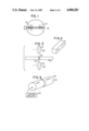
- FIG. 1 is an enlarged top view of a semiconductor wafer showing the positions of adjacent rows of LEDs
- FIG. 2 shows an LED array segment separated from the wafer of FIG. 1;
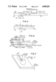
- FIG. 3 shows a cross section of a portion of the wafer of FIG. 1 along with opposing dicing wheels for cutting the wafter;
- FIGS. 4 and 5 show cross section views of a semiconductor wafer cut by a pair of cutting wheels and by prior art techniques respectively;
- FIG. 6 shows a schematic view of cutting apparatus in according with this invention
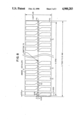
- FIG. 7 shows an enlarged schematic top view of a GaAs wafer including LED arrays abutted in accordance with this invention
- FIG. 8 shows an enlarged top view of a position of an array of LEDs made with the apparatus of FIGS. 6 and 7;
- FIG. 9 shows a projection view of a photosensitive drum along with the positions of a linear LED array in phantom.
- FIG. 1 shows a semiconductor wafer 10 in which LEDs 11 are defined in adjacent rows 12, 13, and so on.
- the LEDs are produced by well understood photolithographic techniques.
- the rows are separated from one another by means discribed for example in U.S. Pat. No. 3,615,047 for an invention of D. Feldman et al.
- the ends of the rows are cut along broken lines 14 and 15 to produce an edge perpendicular to the edge defined by separating the rows of LEDs.
- the number of LEDs in a row such as 12 is limited.
- a semiconductor wafer for example, is typically three inches in diameter, although experimentally wafers have been made having a diameter as much as six inches.
- a copier requires at least eight and one half inches of LEDs to operate effectively to copy paper having a width of eight and one half inches. Not only is a three-inch row of LEDs too short but, also the cuts along broken lines 14 and 15 further reduce the length of the row.
- a linear array of 2048 LEDs can be achieved presently only by abutting several smaller rows of LEDs or by some artifact as described above.
- the invention is based on the recognition that wafer 10 can be cut along lines 14 and 15 so that rows 12 and 13 can be abutted to form a continuous linear array of LEDs longer than can be achieved from a single wafer. In fact, several of such rows can be abutted to provide the accepted 2048 element configuration without staggering or angle-aligning a plurality of segments as described hereinbefore.
- FIG. 3 The dicing of wafer 10 along broken line 14 or 15 in FIG. 1 is depicted in FIG. 3.
- the figure shows portion 20 of wafer 10 positioned so that dicing wheels 21 and 22 oppose one another.
- the wheels are rotated about axes represented by broken lines 23 and 24 and pressed into contact with portion 20 in a manner to make v-shaped cuts 25 and 26 respectively.
- Opposing dicing wheels are well known.
- One description of the use of such opposing wheels for cutting glass panels is desclosed in the IBM Technical Disclosure Bulletin, Vol 21, No 8, January 1979.
- Each dicing wheel has a diameter of six inches (average) and is levelled to produce a 71/2 micron cut from each face of the wafer as shown in FIG. 4.
- FIG. 4 shows wafer portion 40 cut along axis 41; as shown, LED 42 is adjacent an edge having a two-sided bevel made by dicing the wafer by opposing wheels as shown in FIG. 3
- the separation between LEDs in two abutted wafers is depicted in FIG. 4 by showing wafer portion 40 abutted against imaginery wafer portion 44 of an adjacent wafer.
- LED 45 is shown adjacent the cut at 41.
- the damage due to dicing by opposing wheels is limited to less than about ten microns on each side of the cut, so that LEDs 42 and 45 may be placed thirty microns apart.
- FIG. 5 shows a prior art arrangement of a wafer portion 50 similarly positioned with respect to an imaginary second wafer portion 51.
- the wafer portions again are shown in positions dictated as if the two portions 50 and 51 were cut apart by a single dicing wheel from a single wafer.
- the cut is thirty microns, so that adjacent LEDs 53 and 54, on opposite sides of the cut, may be positioned no closer than at least sixty microns.
- FIG. 6 shows apparatus for dicing a semiconductor wafer in the manner discussed in connection with FIG. 4.
- Two dicing wheels 60 and 61 are disposed on axles 62 and 63 respectively, axle 61 being supported by AOU bearing 64 and arm 65.
- the axle are driven by a common drive shaft indicated at 66.
- a wafer to be diced is shown at 67 in FIGS. 6 and 7.
- the wafers are secured to a support jig 68 also shown in FIGS. 6 and 7.
- the support jig has a 50 micron slit 69 in its. Wafers have been diced using a 20 micron cutting wheel in accordance with the present invention in a manner suitable for abuttment as discussed above.
- FIG. 8 shows an enlarged top view of a portion of an array of LEDs made with the apparatus of FIGS. 6 and 7 as shown in FIG. 4.
- the array has 2048 elements defined in 32 chips.
- the array length is 216 mm.
- the resolution is 9.45 dots/mm (240/inch).
- a gallium arsenide (GaAs) chip 70 with a phosphorus diffusion is used.
- Anodes 71 are defined by patterns of aluminum alloy as shown.
- Emitters (LEDs) 73 are defined as shown. The dimensions as shown in the figure are in millimeters.
- Each chip has sixty four LEDs defined on it and adjacent chips are abutted as shown in FIG. 4.
- the thirty two abutted chips are organized into an LED subassembly and juxtaposed with a light-beam transmission and convergence subassembly (not shown) for positioning with respect to photosensitive drum 80 of FIG. 9.
- the position of the subassemblies is represented by the line of circles at 82.
- the organization of the subassemblies with respect to drum 80 is consistent with the teachings of the above noted patent of Tsukada.
- charge coupled devices can be ganged in the same manner to provide a linear scanning with similar advantages.
- the LEDs of a linear array in accordance with this invention are activated simultaneously and the drum is then rotated incrementally to a next position.
- the LEDs are again activated and the process repeated until the entire drum is exposed to produce thereon a latent image for transfer to paper in the familiar manner.
- Circuitry the design of which is well-known in the art, for so activating the LEDs and for incrementing the drum is represented in FIG. 9 by block 90.
Landscapes
- Physics & Mathematics (AREA)
- Optics & Photonics (AREA)
- Health & Medical Sciences (AREA)
- General Health & Medical Sciences (AREA)
- Toxicology (AREA)
- Printers Or Recording Devices Using Electromagnetic And Radiation Means (AREA)
Abstract
Description
Claims (7)
Priority Applications (1)
| Application Number | Priority Date | Filing Date | Title |
|---|---|---|---|
| US07/079,678 US4900283A (en) | 1984-11-26 | 1987-07-30 | Method for arranging chips each having an array of semiconductor light emitting elements |
Applications Claiming Priority (2)
| Application Number | Priority Date | Filing Date | Title |
|---|---|---|---|
| US06/674,592 US4721977A (en) | 1984-11-26 | 1984-11-26 | Electrographic printer with abutting chips each having an array of charge-discharging elements |
| US07/079,678 US4900283A (en) | 1984-11-26 | 1987-07-30 | Method for arranging chips each having an array of semiconductor light emitting elements |
Related Parent Applications (1)
| Application Number | Title | Priority Date | Filing Date |
|---|---|---|---|
| US06/674,592 Continuation US4721977A (en) | 1984-11-26 | 1984-11-26 | Electrographic printer with abutting chips each having an array of charge-discharging elements |
Publications (1)
| Publication Number | Publication Date |
|---|---|
| US4900283A true US4900283A (en) | 1990-02-13 |
Family
ID=26762297
Family Applications (1)
| Application Number | Title | Priority Date | Filing Date |
|---|---|---|---|
| US07/079,678 Expired - Lifetime US4900283A (en) | 1984-11-26 | 1987-07-30 | Method for arranging chips each having an array of semiconductor light emitting elements |
Country Status (1)
| Country | Link |
|---|---|
| US (1) | US4900283A (en) |
Cited By (11)
| Publication number | Priority date | Publication date | Assignee | Title |
|---|---|---|---|---|
| US4997793A (en) * | 1989-11-21 | 1991-03-05 | Eastman Kodak Company | Method of improving cleaving of diode arrays |
| US4997792A (en) * | 1989-11-21 | 1991-03-05 | Eastman Kodak Company | Method for separation of diode array chips during fabrication thereof |
| US5053836A (en) * | 1989-11-21 | 1991-10-01 | Eastman Kodak Company | Cleaving of diode arrays with scribing channels |
| US5221397A (en) * | 1992-11-02 | 1993-06-22 | Xerox Corporation | Fabrication of reading or writing bar arrays assembled from subunits |
| US5580831A (en) * | 1993-07-28 | 1996-12-03 | Fujitsu Limited | Sawcut method of forming alignment marks on two faces of a substrate |
| US5650348A (en) * | 1995-06-07 | 1997-07-22 | Lsi Logic Corporation | Method of making an integrated circuit chip having an array of logic gates |
| US5831218A (en) * | 1996-06-28 | 1998-11-03 | Motorola, Inc. | Method and circuit board panel for circuit board manufacturing that prevents assembly-line delamination and sagging |
| US6271102B1 (en) * | 1998-02-27 | 2001-08-07 | International Business Machines Corporation | Method and system for dicing wafers, and semiconductor structures incorporating the products thereof |
| US20040205970A1 (en) * | 2003-04-17 | 2004-10-21 | Asako Arai | Glass cutter |
| US20050282955A1 (en) * | 2004-06-22 | 2005-12-22 | Marco Apostolo | Fluoroelastomer gels |
| US10242912B2 (en) | 2016-07-08 | 2019-03-26 | Analog Devices, Inc. | Integrated device dies and methods for singulating the same |
Citations (12)
| Publication number | Priority date | Publication date | Assignee | Title |
|---|---|---|---|---|
| GB604494A (en) * | 1945-12-07 | 1948-07-05 | Harold George Ruddick | Improvements in, or relating to, cutting machines |
| US2886748A (en) * | 1954-03-15 | 1959-05-12 | Rca Corp | Semiconductor devices |
| US3615047A (en) * | 1969-06-30 | 1971-10-26 | Bell Telephone Labor Inc | Apparatus and method for separating scribed plates of brittle material |
| SU473683A1 (en) * | 1973-06-14 | 1975-06-14 | Специализированный Трест По Производству Отделочных Работ "Ленотделстрой" | The method of cutting hollow glassware |
| JPS54109375A (en) * | 1978-02-15 | 1979-08-27 | Nec Corp | Cutting method of semiconductor wafer and its unit |
| US4217689A (en) * | 1976-09-14 | 1980-08-19 | Mitsubishi Denki Kabushiki Kaisha | Process for preparing semiconductor devices |
| US4435064A (en) * | 1980-06-28 | 1984-03-06 | Ricoh Co., Ltd. | Optical exposure unit for electrophotographic printing device |
| US4447126A (en) * | 1982-07-02 | 1984-05-08 | International Business Machines Corporation | Uniformly intense imaging by close-packed lens array |
| US4451972A (en) * | 1980-01-21 | 1984-06-05 | National Semiconductor Corporation | Method of making electronic chip with metalized back including a surface stratum of solder |
| US4549784A (en) * | 1982-09-14 | 1985-10-29 | Ricoh Company, Ltd. | Optical fiber-guided scanning device |
| US4553148A (en) * | 1982-06-19 | 1985-11-12 | Olympia Werke Ag | Optical printer for line-by-line image forming |
| JPH06142932A (en) * | 1993-05-20 | 1994-05-24 | Tadahiro Omi | Weld head and welding equipment |
-
1987
- 1987-07-30 US US07/079,678 patent/US4900283A/en not_active Expired - Lifetime
Patent Citations (12)
| Publication number | Priority date | Publication date | Assignee | Title |
|---|---|---|---|---|
| GB604494A (en) * | 1945-12-07 | 1948-07-05 | Harold George Ruddick | Improvements in, or relating to, cutting machines |
| US2886748A (en) * | 1954-03-15 | 1959-05-12 | Rca Corp | Semiconductor devices |
| US3615047A (en) * | 1969-06-30 | 1971-10-26 | Bell Telephone Labor Inc | Apparatus and method for separating scribed plates of brittle material |
| SU473683A1 (en) * | 1973-06-14 | 1975-06-14 | Специализированный Трест По Производству Отделочных Работ "Ленотделстрой" | The method of cutting hollow glassware |
| US4217689A (en) * | 1976-09-14 | 1980-08-19 | Mitsubishi Denki Kabushiki Kaisha | Process for preparing semiconductor devices |
| JPS54109375A (en) * | 1978-02-15 | 1979-08-27 | Nec Corp | Cutting method of semiconductor wafer and its unit |
| US4451972A (en) * | 1980-01-21 | 1984-06-05 | National Semiconductor Corporation | Method of making electronic chip with metalized back including a surface stratum of solder |
| US4435064A (en) * | 1980-06-28 | 1984-03-06 | Ricoh Co., Ltd. | Optical exposure unit for electrophotographic printing device |
| US4553148A (en) * | 1982-06-19 | 1985-11-12 | Olympia Werke Ag | Optical printer for line-by-line image forming |
| US4447126A (en) * | 1982-07-02 | 1984-05-08 | International Business Machines Corporation | Uniformly intense imaging by close-packed lens array |
| US4549784A (en) * | 1982-09-14 | 1985-10-29 | Ricoh Company, Ltd. | Optical fiber-guided scanning device |
| JPH06142932A (en) * | 1993-05-20 | 1994-05-24 | Tadahiro Omi | Weld head and welding equipment |
Non-Patent Citations (5)
| Title |
|---|
| "Diamond Scribers . . . " by L. Curran, Electronics, Nov. 23, 1970, pp. 70-73. |
| "Dicing Techniques--A Survey" by T. D. Bushman, SCP and Solid State Technology, Nov. 1964, pp. 38-42. |
| Diamond Scribers . . . by L. Curran, Electronics, Nov. 23, 1970, pp. 70 73. * |
| Dicing Techniques A Survey by T. D. Bushman, SCP and Solid State Technology, Nov. 1964, pp. 38 42. * |
| IBM Technical Disclosure Bulletin, vol. 21, No. 8, Jan. 1979. * |
Cited By (14)
| Publication number | Priority date | Publication date | Assignee | Title |
|---|---|---|---|---|
| US4997793A (en) * | 1989-11-21 | 1991-03-05 | Eastman Kodak Company | Method of improving cleaving of diode arrays |
| US4997792A (en) * | 1989-11-21 | 1991-03-05 | Eastman Kodak Company | Method for separation of diode array chips during fabrication thereof |
| US5053836A (en) * | 1989-11-21 | 1991-10-01 | Eastman Kodak Company | Cleaving of diode arrays with scribing channels |
| US5300806A (en) * | 1989-11-21 | 1994-04-05 | Eastman Kodak Company | Separation of diode array chips during fabrication thereof |
| US5221397A (en) * | 1992-11-02 | 1993-06-22 | Xerox Corporation | Fabrication of reading or writing bar arrays assembled from subunits |
| US5580831A (en) * | 1993-07-28 | 1996-12-03 | Fujitsu Limited | Sawcut method of forming alignment marks on two faces of a substrate |
| US5650348A (en) * | 1995-06-07 | 1997-07-22 | Lsi Logic Corporation | Method of making an integrated circuit chip having an array of logic gates |
| US5831218A (en) * | 1996-06-28 | 1998-11-03 | Motorola, Inc. | Method and circuit board panel for circuit board manufacturing that prevents assembly-line delamination and sagging |
| US6271102B1 (en) * | 1998-02-27 | 2001-08-07 | International Business Machines Corporation | Method and system for dicing wafers, and semiconductor structures incorporating the products thereof |
| US6600213B2 (en) | 1998-02-27 | 2003-07-29 | International Business Machines Corporation | Semiconductor structure and package including a chip having chamfered edges |
| US6915795B2 (en) | 1998-02-27 | 2005-07-12 | International Business Machines Corporation | Method and system for dicing wafers, and semiconductor structures incorporating the products thereof |
| US20040205970A1 (en) * | 2003-04-17 | 2004-10-21 | Asako Arai | Glass cutter |
| US20050282955A1 (en) * | 2004-06-22 | 2005-12-22 | Marco Apostolo | Fluoroelastomer gels |
| US10242912B2 (en) | 2016-07-08 | 2019-03-26 | Analog Devices, Inc. | Integrated device dies and methods for singulating the same |
Similar Documents
| Publication | Publication Date | Title |
|---|---|---|
| US4721977A (en) | Electrographic printer with abutting chips each having an array of charge-discharging elements | |
| US4900283A (en) | Method for arranging chips each having an array of semiconductor light emitting elements | |
| EP0415795A2 (en) | Method of fabricating full width scanning or imaging arrays from subunits | |
| US4447126A (en) | Uniformly intense imaging by close-packed lens array | |
| EP0798092B1 (en) | Method of slicing semiconductor single crystal ingot | |
| US5128282A (en) | Process for separating image sensor dies and the like from a wafer that minimizes silicon waste | |
| CA1238941A (en) | Geometric led layout for line exposure | |
| EP0786353B1 (en) | Led printing head | |
| US4376282A (en) | Optical print head with graded index fiber arrays for optical printing devices | |
| US6636252B2 (en) | Image exposure apparatus and image forming apparatus with it | |
| US5258629A (en) | Light-emitting diode print head with staggered electrodes | |
| US4534814A (en) | Large-scale printhead for non-impact printer and method of manufacture | |
| CA1236908A (en) | Light emitting diode array and method of producing the same | |
| JP2590988B2 (en) | Optical shutter array | |
| EP0180479B1 (en) | Light-emitting diode array | |
| EP0872892A2 (en) | LED array and printer for an electrophotographic printer with said LED array | |
| EP1275987B1 (en) | Polarization-direction-controlling element and exposure device | |
| EP0310267A2 (en) | Method of alignement of led chips | |
| JP2003218471A (en) | Method of generating laser diode | |
| JPS58203071A (en) | Light emitting diode array | |
| US4675572A (en) | Write head of optical printer | |
| JPH0542718A (en) | Semiconductor light emitting device | |
| JPH06112526A (en) | Semiconductor chip array, semiconductor chip forming pattern therefor, and its dicing method | |
| JP2007276183A (en) | Light emitting element array chip with microlens and optical writing head | |
| JP2008227071A (en) | Semiconductor light emitting element array chip, manufacturing method thereof, and exposure light source device |
Legal Events
| Date | Code | Title | Description |
|---|---|---|---|
| AS | Assignment |
Owner name: KENTEK INFORMATION SYSTEMS, INC., SIX PEARL COURT Free format text: ASSIGNMENT OF ASSIGNORS INTEREST.;ASSIGNOR:FUKAE, KENSUKE;REEL/FRAME:004760/0916 Effective date: 19870810 Owner name: KENTEK INFORMATION SYSTEMS, INC.,NEW JERSEY Free format text: ASSIGNMENT OF ASSIGNORS INTEREST;ASSIGNOR:FUKAE, KENSUKE;REEL/FRAME:004760/0916 Effective date: 19870810 |
|
| STCF | Information on status: patent grant |
Free format text: PATENTED CASE |
|
| FPAY | Fee payment |
Year of fee payment: 4 |
|
| FEPP | Fee payment procedure |
Free format text: PAYOR NUMBER ASSIGNED (ORIGINAL EVENT CODE: ASPN); ENTITY STATUS OF PATENT OWNER: LARGE ENTITY |
|
| FPAY | Fee payment |
Year of fee payment: 8 |
|
| AS | Assignment |
Owner name: INTEL CORPORATION, A DELAWARE CORPORATION, CALIFOR Free format text: ASSIGNMENT OF ASSIGNORS INTEREST;ASSIGNOR:KENTEK INFORMATION SYSTEMS, INC.;REEL/FRAME:010579/0508 Effective date: 19991130 |
|
| FEPP | Fee payment procedure |
Free format text: PAYER NUMBER DE-ASSIGNED (ORIGINAL EVENT CODE: RMPN); ENTITY STATUS OF PATENT OWNER: LARGE ENTITY Free format text: PAYOR NUMBER ASSIGNED (ORIGINAL EVENT CODE: ASPN); ENTITY STATUS OF PATENT OWNER: LARGE ENTITY |
|
| FPAY | Fee payment |
Year of fee payment: 12 |