US4870620A - Dynamic random access memory device with internal refresh - Google Patents
Dynamic random access memory device with internal refresh Download PDFInfo
- Publication number
- US4870620A US4870620A US07/141,076 US14107688A US4870620A US 4870620 A US4870620 A US 4870620A US 14107688 A US14107688 A US 14107688A US 4870620 A US4870620 A US 4870620A
- Authority
- US
- United States
- Prior art keywords
- random access
- access memory
- input
- dynamic random
- voltage
- Prior art date
- Legal status (The legal status is an assumption and is not a legal conclusion. Google has not performed a legal analysis and makes no representation as to the accuracy of the status listed.)
- Expired - Lifetime
Links
Images


Classifications
-
- G—PHYSICS
- G11—INFORMATION STORAGE
- G11C—STATIC STORES
- G11C8/00—Arrangements for selecting an address in a digital store
- G11C8/06—Address interface arrangements, e.g. address buffers
-
- G—PHYSICS
- G11—INFORMATION STORAGE
- G11C—STATIC STORES
- G11C11/00—Digital stores characterised by the use of particular electric or magnetic storage elements; Storage elements therefor
- G11C11/21—Digital stores characterised by the use of particular electric or magnetic storage elements; Storage elements therefor using electric elements
- G11C11/34—Digital stores characterised by the use of particular electric or magnetic storage elements; Storage elements therefor using electric elements using semiconductor devices
- G11C11/40—Digital stores characterised by the use of particular electric or magnetic storage elements; Storage elements therefor using electric elements using semiconductor devices using transistors
- G11C11/401—Digital stores characterised by the use of particular electric or magnetic storage elements; Storage elements therefor using electric elements using semiconductor devices using transistors forming cells needing refreshing or charge regeneration, i.e. dynamic cells
- G11C11/406—Management or control of the refreshing or charge-regeneration cycles
Definitions
- the present invention relates to a dynamic random access memory device having a self-refresh function and, more specifically, it relates to a random access memory device capable of performing a self-refresh operation without a malfunction.
- FIG. 1A is a block diagram showing an example of a simplified circuit of a conventional 1 M bit dynamic RAM (Random Access Memory) having 1048576 memory cells.
- a summary of the basic operation of the dynamic RAM and the "CAS before RAS Refresh" function in relation to the present invention will be hereinafter described.
- a clock generator 151 receives an RAS (Row Address Strobe) signal, CAS (Column Address Strobe) signal and WE (Write Enable) signal from a CPU (Central Processing Unit) and generates clock signals ⁇ 0 and ⁇ 1 .
- an address buffer 1 receives external address signals EXT. A 0 to A 9 on a time share basis through a switching circuit 4 and applies internal address signals A 0 to A 8 on a time share basis to a row decoder 155 and a column decoder 156.
- the row decoder 155 and the column decoder 156 decode the internal address signals A 0 to A 8 and apply the decoded signals to a memory cell array 158 and an I/O gates 157.
- the writing operation of the input data D IN and the reading operation of the output data D OUT are carried out for a memory cell having the address designated as described above.
- An input buffer 159 receives the input data D IN and transfers the input data D IN to the memory cell array 158 via the I/0 gates 157 and the sense amplifiers 163 in response to a clock signal ⁇ 3 .
- the output buffer 160 receives the data from the memory cell array 158 via the sense amplifiers 163 and the I/O gates 157 and outputs the output data D OUT in response to the clock signal ⁇ 3 .
- a refresh controller 152 In the dynamic RAM, as is generally known, the reading and rewriting operation of all the memory cells, that is, the refresh operation, is carried out during the intervals of the above described usual read/write operation.
- a refresh controller 152 in a refresh operation a refresh controller 152 generates a driving signal T for driving a refresh counter 2 in response to a clock signal ⁇ 0 from the clock generator 151.
- the refresh counter 2 receives the driving signal T and performs count operation and applies the output signals Q 0 to Q 8 to the address buffer 1 through the switching circuit 4.
- the address buffer 1 receives the output signals Q 0 to Q 8 of the refresh counter 2 instead of the external address signals EXT.
- the reading operation of already written data and the rewriting operation are carried out successively for the memory cells having the addresses designated by the internal address signals A 0 to A 8 . Since the refresh counter 2 successively outputs the output signals, the refresh of all memory cells can be accomplished by the repetition of the above described operation.
- the method for performing refreshing in which the signals for refreshing are not applied externally as the external address signals EXT.
- a 9 but the signals are generated by the refresh counter 2 provided in the chip, is called "CAS before RAS Refresh", which is an almost standard function of a dynamic RAM.
- the switching circuit 4 selects either the external address signals EXT. A 0 to EXT A 8 or the output signals Q 0 to Q 8 of the refresh counter 2 in response to the clock signals ⁇ 2 and ⁇ 2 and applies the same to the address buffer 1.
- the operation state of the dynamic RAM comprises the normal read/write operation stat, "CAS before RAS Refresh" operation state and, further a standby state which is the state other than the above mentioned two operation states of the dynamic RAM. These three states are specified by the RAS signal and the CAS signal.
- FIG. 1B is a timing chart showing the relation between the RAS signal, CAS signal and other signals and the three states of the dynamic RAM.
- the clock signals ⁇ 2 and ⁇ 2 are the signals required for the operation of the switching circuit 4 and they are applied to the switching circuit 4 from the clock generator 151 through the refresh controller 152.
- the dynamic RAM when the RAS signal and the CAS signal simultaneously become high level, the dynamic RAM is in the standby state.
- the clock signals ⁇ 2 and ⁇ 2 have the voltages of low level and high level, respectively.
- the CAS signal becomes low level and thereafter the RAS signal becomes low level
- the "CAS before RAS Refresh" operation starts in the dynamic RAM.
- both inverted clock signals ⁇ 2 and ⁇ 2 are applied to the switching circuit 4.
- the dynamic RAM is in the standby state initially, and the CAS signal becomes low level after the RAS signal becomes low level, the normal read/write operation of the dynamic RAM starts.
- the RAS signal is at the low level, it is called the activated state.
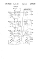
- FIG. 2A is a schematic diagram showing the conventional switching circuit 4 and the peripheral circuits thereof shown in FIG. 1A.
- FIG. 2A comprises nine circuit portions having similar connections. In the following, the description will be made only of the i-th circuit portion for the simplicity of the description, and the description can be applied to other circuit portions.
- Ai is connected to one input of the switching circuit 4 through an n type field effect transistor 3.
- a clock signal ⁇ 1 is applied to the gate of the transistor 3 from the clock generator.
- the clock signal ⁇ 1 becomes high level in the standby state.
- the refresh counter 2 is connected to the other input of the switching circuit 4.
- the output of the switching circuit 4 is connected to the address buffer 1.
- the switching circuit 4 comprises an n type field effect transistor 40 connected to the transistor 3 and an n type field effect transistor 41 connected to the refresh counter 2.
- the node of the transistors 40 and 41 constitute the output of the switching circuit 4.
- a clock signal ⁇ 2 is applied to the gate of the transistor 41 and the inverted signal ⁇ 2 of the clock signal ⁇ 2 is applied to the gate of the transistor 40, respectively.
- the clock signals ⁇ 2 and ⁇ 2 are applied to the transistors 40 and 41 both from the clock generator through the refresh controller.
- the refresh counter 2 a series connection in the output stage of the n type field effect transistors 20 and 21 connected between the power supply V cc and the ground V ss is schematically shown.
- an n type MOS field effect transistor 10 in the input stage and a capacitor 11 for holding voltage are schematically shown.
- the address buffer 1 outputs the i-th internal address signal A i out of 0 to 9 and the inverted signal thereof, A i .
- V b denotes the voltage of the input of the address buffer 1.
- Q i is the i-th output signal of the refresh counter 2.
- the switching circuit 4 selectively applies either the external address signal EXT. Ai or the output signal Q i of the refresh counter to the input of the address buffer 1 in response to the clock signals ⁇ 2 and ⁇ 2 .
- FIG. 2B is a timing chart showing the changes in each of the signals in the i-th circuit portion of the circuit shown in FIG. 2A.
- the clock signal ⁇ 1 is at the H level
- the clock signal ⁇ 2 is at the L level
- the clock signal ⁇ 2 is at the H level, so that the external address signal EXT.
- Ai is applied to the input of the address buffer 1 through the transistor 40 of the switching circuit 4.
- the voltage of the external address signal EXT. Ai is 0 volt.
- the input of the address buffer 1 is brought to the voltage of 0 volt (reference should be made to the waveform of V b in FIG. 2B).
- the input of the address buffer 1 receives the output signal Q i of the refresh counter 2 instead of the external address signal EXT. Ai through the switching circuit 4.
- the output signal Q i of the refresh counter 2 is at the H level, the input voltage V b of the address buffer 1 begins to rise (reference should be made to the waveform of V b of FIG. 2B).
- the address buffer 1 starts the operation.
- EXT. A is an externally applied signal
- EXT. A can assume a lower voltage representing the low logic level. This is because the external circuit supplying EXT. A, may be operated at a slightly different supply voltage or the signal may contain noise. Such an occurrence is well-recognized and memories are commonly rated at a -1.0 to -2.0 volt lower limit to be recognized as a low logic level.
- the voltage of the external address signal EXT. Ai is for example -2.0 volt, which is the lowest voltage enabling the external address signal EXT. Ai to be recognized as the logic low level.
- the input of the address buffer 1 is brought to the voltage of -2.0 volt (reference should be made to the dotted line in FIG. 2B).
- the input voltage V b of the address buffer 1 is not brought to the voltage which can be recognized by the address buffer 1 as the logic high level at the time t 3 , that is, the time when the address buffer 1 begins the operation.
- the address buffer 1 can not receive the correct signal from the refresh counter 2, the "CAS before RAS Refresh" operation, for example, is not carried out correctly.
- the capacitor 11 of the address buffer 1 is to maintain the voltage of the external address signal EXT. Ai applied to the input of the address buffer 1. Namely, when the voltage of the external address signal EXT. Ai is applied to the input of the address buffer 1, the capacitor 11 is charged. Thereafter, the transistor 3 turns off in response to the clock signal ⁇ 1 and the input of the address buffer 1 is brought to the floating state. The capacitor 11 continues to apply the charged voltage to the gate of the transistor 10 during the operation of the address buffer 1. Therefore, the external address signal EXT. Ai need not be continuously applied to the input terminal 9.
- a main object of the present invention is to provide a dynamic random access memory device capable of operating the refresh counter means without malfunctioning by correctly transmitting the signals from the refresh counter means to the address buffer means.
- the present invention comprises selective output means having one input connected to receive the signals applied to the external address input and other input connected to receive the signals from the refresh counter means for selectively outputting either of the signals to the address buffer means connected to the output thereof in response to a first clock signal, and voltage supply means connected to the one input of the selective output means for applying a predetermined level voltage to the one input.
- the selective means switches in response to the first clock signal so as to apply the signal from the refresh counter means to the address buffer means. Therefore, the signal from the refresh counter means is correctly transmitted to the address buffer means, so that the address buffer means operates correctly.
- the address buffer means since the address buffer means operates correctly without malfunctioning, the reliability of the refresh operation can be enhanced.
- the voltage supply means comprises voltage setting means for applying a voltage of the reference voltage point in response to a second clock signal.
- the voltage setting means applies the voltage of the reference voltage point to the address buffer means in response to the second clock signal. Consequently, malfunctions of the address buffer means can be prevented.
- the voltage supply means comprises voltage changing means for changing the voltage level of the external address input to a predetermined voltage level.
- the voltage changing means converts the voltage of the external address input to a predetermined voltage level and applies the same to the address buffer means. Therefore, malfunctions of the address buffer means can be prevented.
- FIG. 1A is a schematic block diagram showing one example of the structure of a conventional dynamic RAM
- FIG. 1B is a timing chart showing the relation between main signals and the operation states of the dynamic RAM shown in FIG. 1A;
- FIG. 2A is a schematic diagram showing the switching circuit and the peripheral circuits thereof in the conventional dynamic RAM shown in FIG. 1A;
- FIG. 2B is a timing chart of each of the signals for the description of the circuit shown in FIG. 2A;
- FIG. 3A is a schematic diagram of one embodiment of the switching circuit and the peripheral circuit thereof of the dynamic RAM in accordance with the present invention.
- FIG. 3B is a timing chart of each of the signals employed in the description of the circuit shown in FIG. 3A;
- FIG. 4 is a part of a circuit diagram showing another embodiment of the switching circuit and the peripheral circuit thereof in the dynamic RAM in accordance with the present invention
- FIG. 5 is a part of the circuit diagram showing further embodiment of the switching circuit and a peripheral circuit thereof in the dynamic RAM in accordance with the present invention.
- FIG. 6 is a part of the circuit diagram showing a further embodiment of the switching circuit and a peripheral circuit thereof in the dynamic RAM in accordance with the present invention.
- FIG. 3A is a schematic diagram showing one embodiment of the switching circuit and the peripheral circuit thereof in the dynamic RAM in accordance with the present invention.
- the i-th circuit portion will be employed for the simplicity of the description, as in the case of FIG. 2A, and the description can be applied to other circuit portions.
- the circuit shown in FIG. 3A further comprises an n type filed effect transistor 54 connected between the input of the transistor 3 and the ground V ss , and a clock signal ⁇ 3 is applied to the gate of the transistor 54.
- the clock signal ⁇ 3 is almost in synchronization with the RAS signal and becomes H level during the standby period. Since other portions of the circuit of FIG. 3A are the same as the conventional circuit shown in FIG. 2A, and has been described above, the description thereof will not be repeated here.
- FIG. 3B is a timing chart showing the changes in each of the signals in the circuit shown in FIG. 3A.
- the dynamic RAM is in the standby state.
- the clock signal ⁇ 1 is at the H level
- the clock signal ⁇ 2 is at the L level
- the clock signal ⁇ 2 is at the H level
- the clock signal ⁇ 3 is at the H level.
- the transistor 54 turns on in response to the clock signal ⁇ 3 and brings the input of the transistor 3 to the voltage of the ground V ss level. Therefore, even if the input terminal 9 receives the external address signal EXT.
- the input of the address buffer 1 is brought to the voltage of the ground V ss level applied through the transistor 3 and the switching circuit 4, since the input of the transistor 3 is brought to the voltage of the ground V ss level.
- the "CAS before RAS Refresh" state of the dynamic RAM begins.
- the clock signal ⁇ 2 changes to the H level while the clock signal ⁇ 2 changes to the L level.
- the transistor 40 turns off in response to the clock signal ⁇ 2 and the transistor 41 turns on in response to the clock signal ⁇ 2 .
- the output signal Q i of the refresh counter 2 is applied to the input of the address buffer 1 through the transistor 41.
- the output signal Q i of the refresh counter 2 has the voltage of H level, the input voltage V b of the address buffer rises (reference should be made to the waveform V b of FIG. 3B).
- the address buffer 1 begins the operation.
- the transistor 54 is connected between the input of the transistor 3 and ground V ss , one electrode of the transistor 54 may be connected to the power supply V cc instead of the ground V ss to obtain a similarly advantageous result.
- FIG. 4 is a partial circuit diagram showing another embodiment of the switching circuit and the peripheral circuit of the dynamic RAM of the present invention.
- the circuit diagram of FIG. 4 includes only the i-th circuit portion for simplicity.
- the circuit of FIG. 4 further comprises an inverter circuit 5 comprising two inverters connected between the input terminal 9 and the input of the transistor 3.
- the inverter circuit 5 is a voltage changing circuit for changing the voltage of the signal applied to the input terminal 9 to the voltage level of the power supply V cc or of the ground V ss .
- the inverter of the preceding stage comprises a series connection of n type field effect transistors 50 and 51 connected between the power supply V cc and the ground V ss .
- the inverter in the succeeding stage comprises a series connection of the n type field effect transistors 52 and 53 connected between the power supply V cc and the ground V ss .
- the gates of the transistors 50 and 52 are both connected to the power supply V cc .
- the gate of the transistor 51 is connected to the input terminal 9.
- the gate of the transistor 53 is connected to the node connected to the transistors 50 and 51.
- the node connected to the transistors 52 and 53 is connected to the input of the transistor 3.
- the clock signal ⁇ 1 is at the H level
- the clock signal ⁇ 2 is at the L level
- the clock signal ⁇ 2 is at the H level.
- the external address signal EXT. Ai is applied to the input of the address buffer 1 through the buffer circuit 5, transistor 3 and the switching circuit 4. Even if the input terminal 9 is brought to the voltage of, for example -2.0 volt upon receipt of the external address signal EXT. Ai, the inverter circuit 5 comprising two inverters outputs the voltage of the ground V ss level. Therefore, the input of the address buffer 1 is brought to the voltage of the ground V ss level applied through the transistor 3 and the switching circuit 4. The operation of the circuit shown in FIG.
- the inverter circuit 5 comprises a two-stage inverter in the circuit of FIG. 4, the same result will be brought about by a one-stage inverter.
- the inverted signal of the external address signal EXT. Ai is applied to the input of the address buffer 1.
- FIG. 5 shows a partial circuit diagram showing another embodiment of the switching circuit and the peripheral circuit of the dynamic RAM using these two inventions. Similar to FIG. 4, the circuit diagram of FIG. 5 comprises only the i-th circuit portion for simplicity.
- the circuit of FIG. 5 further comprises a one-stage inverter connected between the input terminal 9 and the input of the transistor 3.
- the inverter comprises a series connection of the n type field effect transistors 50 and 51 connected between the power supply V cc and the ground V ss .
- the gate of the transistor 50 is connected to the power supply V cc and the gate of the transistor 51 is connected to the input terminal 9.
- the node connected to the transistors 50 and 51 is connected to the input of the transistor 3.
- FIG. 6 shows a partial circuit diagram showing a further embodiment of the switching circuit and the peripheral circuit of the dynamic RAM utilizing these two inventions.
- the circuit of FIG. 6 comprises complementary field effect transistors, and the switching circuit 4 comprises transmission gates 58 and 59 instead of the transistors 40 and 41.
- the inverter comprises a series connection of the p type field effect transistors 55 and 56 and the n type field effect transistor 57 connected between the power supply V cc and the ground V ss .
- the clock signal ⁇ 3 is applied to the gate of the transistor 55.
- the gates of the transistors 56 and 57 are connected together to the input terminal 9.
- the node connected to the transistors 56 and 57 is connected to the input of the transistor 3. Since the address buffer 1 has the same function as the transistor 3 shown in FIG. 5, the transistor 3 is not necessary in the circuit of FIG. 6.
- the present invention comprises switching means for applying either the signals from the external address input or the signals from the refresh counter means to the address buffer means in response to the first clock signal and voltage supply means for applying the voltage of a predetermined level to the input of the switching means for receiving the signal from the external address input.
- the voltage supply means applies the predetermined voltage to the address buffer means. Therefore, malfunction of the address buffer means can be prevented and the reliability of the refresh operation is enhanced.
Landscapes
- Engineering & Computer Science (AREA)
- Microelectronics & Electronic Packaging (AREA)
- Computer Hardware Design (AREA)
- Dram (AREA)
Abstract
Description
Claims (26)
Applications Claiming Priority (4)
| Application Number | Priority Date | Filing Date | Title |
|---|---|---|---|
| JP62-842 | 1987-01-06 | ||
| JP62000842A JPS63168897A (en) | 1987-01-06 | 1987-01-06 | Dynamic ram |
| JP62179361A JPH0793001B2 (en) | 1987-07-17 | 1987-07-17 | Dynamic RAM |
| JP62-179361 | 1987-07-17 |
Publications (1)
| Publication Number | Publication Date |
|---|---|
| US4870620A true US4870620A (en) | 1989-09-26 |
Family
ID=26333939
Family Applications (1)
| Application Number | Title | Priority Date | Filing Date |
|---|---|---|---|
| US07/141,076 Expired - Lifetime US4870620A (en) | 1987-01-06 | 1988-01-05 | Dynamic random access memory device with internal refresh |
Country Status (1)
| Country | Link |
|---|---|
| US (1) | US4870620A (en) |
Cited By (6)
| Publication number | Priority date | Publication date | Assignee | Title |
|---|---|---|---|---|
| US4951258A (en) * | 1988-07-07 | 1990-08-21 | Oki Electric Industry Co., Ltd. | Dynamic random access memory system including predecoder means |
| WO1990016029A1 (en) * | 1989-06-12 | 1990-12-27 | Grid Systems Corporation | Low-power, standby mode computer |
| US5270982A (en) * | 1991-04-30 | 1993-12-14 | Nec Corporation | Dynamic random access memory device improved in testability without sacrifice of current consumption |
| US5426613A (en) * | 1989-03-20 | 1995-06-20 | Hitachi, Ltd. | Semiconductor memory device with improved substrate arrangement to permit forming a plurality of different types of random access memory, and a testing method therefor |
| US5430686A (en) * | 1992-07-09 | 1995-07-04 | Mitsubishi Denki Kabushiki Kaisha | Semiconductor memory device and operating method thereof |
| US6157581A (en) * | 1998-08-12 | 2000-12-05 | Nec Corporation | Semiconductor memory having a restore voltage control circuit |
Citations (6)
| Publication number | Priority date | Publication date | Assignee | Title |
|---|---|---|---|---|
| US4207618A (en) * | 1978-06-26 | 1980-06-10 | Texas Instruments Incorporated | On-chip refresh for dynamic memory |
| US4570242A (en) * | 1981-10-27 | 1986-02-11 | Nippon Electric Co., Ltd. | Dynamic random-access memory |
| US4628482A (en) * | 1982-05-07 | 1986-12-09 | Hitachi, Ltd. | Common memory control system with two bus masters |
| US4631701A (en) * | 1983-10-31 | 1986-12-23 | Ncr Corporation | Dynamic random access memory refresh control system |
| US4677592A (en) * | 1984-05-31 | 1987-06-30 | Kabushiki Kaisha Toshiba | Dynamic RAM |
| US4682306A (en) * | 1984-08-20 | 1987-07-21 | Kabushiki Kaisha Toshiba | Self-refresh control circuit for dynamic semiconductor memory device |
-
1988
- 1988-01-05 US US07/141,076 patent/US4870620A/en not_active Expired - Lifetime
Patent Citations (7)
| Publication number | Priority date | Publication date | Assignee | Title |
|---|---|---|---|---|
| US4207618A (en) * | 1978-06-26 | 1980-06-10 | Texas Instruments Incorporated | On-chip refresh for dynamic memory |
| US4207618B1 (en) * | 1978-06-26 | 1989-04-18 | ||
| US4570242A (en) * | 1981-10-27 | 1986-02-11 | Nippon Electric Co., Ltd. | Dynamic random-access memory |
| US4628482A (en) * | 1982-05-07 | 1986-12-09 | Hitachi, Ltd. | Common memory control system with two bus masters |
| US4631701A (en) * | 1983-10-31 | 1986-12-23 | Ncr Corporation | Dynamic random access memory refresh control system |
| US4677592A (en) * | 1984-05-31 | 1987-06-30 | Kabushiki Kaisha Toshiba | Dynamic RAM |
| US4682306A (en) * | 1984-08-20 | 1987-07-21 | Kabushiki Kaisha Toshiba | Self-refresh control circuit for dynamic semiconductor memory device |
Non-Patent Citations (4)
| Title |
|---|
| Eaton, S. Sheffield, IEEE International Solid State Conference, "A 5V-only 2Kx8 Dynamic Ram", Feb. 15, 1987, pp. 144-145. |
| Eaton, S. Sheffield, IEEE International Solid State Conference, A 5V only 2Kx8 Dynamic Ram , Feb. 15, 1987, pp. 144 145. * |
| Ford, David C. et al, Electronics, "64-K Dynamic RAM Has Pin That Refreshes", Feb. 15, 1979, pp. 141-147. |
| Ford, David C. et al, Electronics, 64 K Dynamic RAM Has Pin That Refreshes , Feb. 15, 1979, pp. 141 147. * |
Cited By (6)
| Publication number | Priority date | Publication date | Assignee | Title |
|---|---|---|---|---|
| US4951258A (en) * | 1988-07-07 | 1990-08-21 | Oki Electric Industry Co., Ltd. | Dynamic random access memory system including predecoder means |
| US5426613A (en) * | 1989-03-20 | 1995-06-20 | Hitachi, Ltd. | Semiconductor memory device with improved substrate arrangement to permit forming a plurality of different types of random access memory, and a testing method therefor |
| WO1990016029A1 (en) * | 1989-06-12 | 1990-12-27 | Grid Systems Corporation | Low-power, standby mode computer |
| US5270982A (en) * | 1991-04-30 | 1993-12-14 | Nec Corporation | Dynamic random access memory device improved in testability without sacrifice of current consumption |
| US5430686A (en) * | 1992-07-09 | 1995-07-04 | Mitsubishi Denki Kabushiki Kaisha | Semiconductor memory device and operating method thereof |
| US6157581A (en) * | 1998-08-12 | 2000-12-05 | Nec Corporation | Semiconductor memory having a restore voltage control circuit |
Similar Documents
| Publication | Publication Date | Title |
|---|---|---|
| US5297104A (en) | Word line drive circuit of semiconductor memory device | |
| US5812015A (en) | Boosting pulse generation circuit for a semiconductor integrated circuit | |
| US5412331A (en) | Word line driving circuit of a semiconductor memory device | |
| US5119334A (en) | Dynamic random access memory having improved word line control | |
| US4661928A (en) | Output buffer in which inductive noise is suppressed | |
| KR920008032B1 (en) | Operation mode setting circuit | |
| EP0056240B1 (en) | Memory device | |
| US6335895B1 (en) | Semiconductor storage device and system using the same | |
| US4688196A (en) | Semiconductor dynamic memory device with less power consumption in internal refresh mode | |
| US4281401A (en) | Semiconductor read/write memory array having high speed serial shift register access | |
| US5696721A (en) | Dynamic random access memory having row decoder with level translator for driving a word line voltage above and below an operating supply voltage range | |
| US5936910A (en) | Semiconductor memory device having burn-in test function | |
| US4788457A (en) | CMOS row decoder circuit for use in row and column addressing | |
| US5808482A (en) | Row decoder with level translator | |
| GB2341706A (en) | Synchronous semiconductor memory device with a clock generating circuit | |
| US5291454A (en) | Circuit for decreasing current consumption in data output circuit in case one of two supply voltages fails | |
| US4797573A (en) | Output circuit with improved timing control circuit | |
| US5208777A (en) | Semiconductor memory device | |
| US4870620A (en) | Dynamic random access memory device with internal refresh | |
| US4811304A (en) | MDS decoder circuit with high voltage suppression of a decoupling transistor | |
| EP0062547A2 (en) | Memory circuit | |
| US5418756A (en) | Edge transition detection disable circuit to alter memory device operating characteristics | |
| US5420869A (en) | Semiconductor integrated circuit device | |
| US4485461A (en) | Memory circuit | |
| US6288573B1 (en) | Semiconductor device capable of operating fast with a low voltage and reducing power consumption during standby |
Legal Events
| Date | Code | Title | Description |
|---|---|---|---|
| AS | Assignment |
Owner name: MITSUBISHI DENKI KABUSHIKI KAISHA,JAPAN Free format text: ASSIGNMENT OF ASSIGNORS INTEREST;ASSIGNORS:YAMAGATA, TADATO;MIYAMOTO, HIROSHI;YAMADA, MICHIHIRO;AND OTHERS;REEL/FRAME:004843/0722 Effective date: 19871225 Owner name: MITSUBISHI DENKI KABUSHIKI KAISHA, 2-3 MARUNOUCHI Free format text: ASSIGNMENT OF ASSIGNORS INTEREST.;ASSIGNORS:YAMAGATA, TADATO;MIYAMOTO, HIROSHI;YAMADA, MICHIHIRO;AND OTHERS;REEL/FRAME:004843/0722 Effective date: 19871225 |
|
| STCF | Information on status: patent grant |
Free format text: PATENTED CASE |
|
| FEPP | Fee payment procedure |
Free format text: PAYOR NUMBER ASSIGNED (ORIGINAL EVENT CODE: ASPN); ENTITY STATUS OF PATENT OWNER: LARGE ENTITY |
|
| FPAY | Fee payment |
Year of fee payment: 4 |
|
| CC | Certificate of correction | ||
| FPAY | Fee payment |
Year of fee payment: 8 |
|
| FPAY | Fee payment |
Year of fee payment: 12 |