US4861393A - Semiconductor heterostructures having Gex Si1-x layers on Si utilizing molecular beam epitaxy - Google Patents

Semiconductor heterostructures having Gex Si1-x layers on Si utilizing molecular beam epitaxy Download PDF

Info

Publication number
US4861393A
US4861393A US07/057,679 US5767987A US4861393A US 4861393 A US4861393 A US 4861393A US 5767987 A US5767987 A US 5767987A US 4861393 A US4861393 A US 4861393A
Authority
US
United States
Prior art keywords
layer
layers
growth
substrate
films
Prior art date
Legal status (The legal status is an assumption and is not a legal conclusion. Google has not performed a legal analysis and makes no representation as to the accuracy of the status listed.)
Expired - Lifetime
Application number
US07/057,679
Inventor
John C. Bean
Leonard C. Feldman
Anthony T. Fiory
Current Assignee (The listed assignees may be inaccurate. Google has not performed a legal analysis and makes no representation or warranty as to the accuracy of the list.)
Nokia Bell Labs USA
Agere Systems LLC
Original Assignee
AT&T Bell Laboratories Inc
Priority date (The priority date is an assumption and is not a legal conclusion. Google has not performed a legal analysis and makes no representation as to the accuracy of the date listed.)
Filing date
Publication date
Priority claimed from US06/546,736 external-priority patent/US4529455A/en
Application filed by AT&T Bell Laboratories Inc filed Critical AT&T Bell Laboratories Inc
Priority to US07/057,679 priority Critical patent/US4861393A/en
Application granted granted Critical
Publication of US4861393A publication Critical patent/US4861393A/en
Assigned to AGERE SYSTEMS INC. reassignment AGERE SYSTEMS INC. ASSIGNMENT OF ASSIGNORS INTEREST (SEE DOCUMENT FOR DETAILS). Assignors: LUCENT TECHNOLOGIES INC., AT&T CORP.
Anticipated expiration legal-status Critical
Expired - Lifetime legal-status Critical Current

Links

Images

Classifications

    • HELECTRICITY
    • H10SEMICONDUCTOR DEVICES; ELECTRIC SOLID-STATE DEVICES NOT OTHERWISE PROVIDED FOR
    • H10DINORGANIC ELECTRIC SEMICONDUCTOR DEVICES
    • H10D62/00Semiconductor bodies, or regions thereof, of devices having potential barriers
    • H10D62/80Semiconductor bodies, or regions thereof, of devices having potential barriers characterised by the materials
    • H10D62/82Heterojunctions
    • H10D62/822Heterojunctions comprising only Group IV materials heterojunctions, e.g. Si/Ge heterojunctions
    • H10P14/22
    • H10P14/2905
    • H10P14/3211
    • H10P14/3248
    • H10P14/3411
    • YGENERAL TAGGING OF NEW TECHNOLOGICAL DEVELOPMENTS; GENERAL TAGGING OF CROSS-SECTIONAL TECHNOLOGIES SPANNING OVER SEVERAL SECTIONS OF THE IPC; TECHNICAL SUBJECTS COVERED BY FORMER USPC CROSS-REFERENCE ART COLLECTIONS [XRACs] AND DIGESTS
    • Y10TECHNICAL SUBJECTS COVERED BY FORMER USPC
    • Y10STECHNICAL SUBJECTS COVERED BY FORMER USPC CROSS-REFERENCE ART COLLECTIONS [XRACs] AND DIGESTS
    • Y10S148/00Metal treatment
    • Y10S148/025Deposition multi-step
    • YGENERAL TAGGING OF NEW TECHNOLOGICAL DEVELOPMENTS; GENERAL TAGGING OF CROSS-SECTIONAL TECHNOLOGIES SPANNING OVER SEVERAL SECTIONS OF THE IPC; TECHNICAL SUBJECTS COVERED BY FORMER USPC CROSS-REFERENCE ART COLLECTIONS [XRACs] AND DIGESTS
    • Y10TECHNICAL SUBJECTS COVERED BY FORMER USPC
    • Y10STECHNICAL SUBJECTS COVERED BY FORMER USPC CROSS-REFERENCE ART COLLECTIONS [XRACs] AND DIGESTS
    • Y10S148/00Metal treatment
    • Y10S148/059Germanium on silicon or Ge-Si on III-V
    • YGENERAL TAGGING OF NEW TECHNOLOGICAL DEVELOPMENTS; GENERAL TAGGING OF CROSS-SECTIONAL TECHNOLOGIES SPANNING OVER SEVERAL SECTIONS OF THE IPC; TECHNICAL SUBJECTS COVERED BY FORMER USPC CROSS-REFERENCE ART COLLECTIONS [XRACs] AND DIGESTS
    • Y10TECHNICAL SUBJECTS COVERED BY FORMER USPC
    • Y10STECHNICAL SUBJECTS COVERED BY FORMER USPC CROSS-REFERENCE ART COLLECTIONS [XRACs] AND DIGESTS
    • Y10S148/00Metal treatment
    • Y10S148/067Graded energy gap
    • YGENERAL TAGGING OF NEW TECHNOLOGICAL DEVELOPMENTS; GENERAL TAGGING OF CROSS-SECTIONAL TECHNOLOGIES SPANNING OVER SEVERAL SECTIONS OF THE IPC; TECHNICAL SUBJECTS COVERED BY FORMER USPC CROSS-REFERENCE ART COLLECTIONS [XRACs] AND DIGESTS
    • Y10TECHNICAL SUBJECTS COVERED BY FORMER USPC
    • Y10STECHNICAL SUBJECTS COVERED BY FORMER USPC CROSS-REFERENCE ART COLLECTIONS [XRACs] AND DIGESTS
    • Y10S148/00Metal treatment
    • Y10S148/072Heterojunctions
    • YGENERAL TAGGING OF NEW TECHNOLOGICAL DEVELOPMENTS; GENERAL TAGGING OF CROSS-SECTIONAL TECHNOLOGIES SPANNING OVER SEVERAL SECTIONS OF THE IPC; TECHNICAL SUBJECTS COVERED BY FORMER USPC CROSS-REFERENCE ART COLLECTIONS [XRACs] AND DIGESTS
    • Y10TECHNICAL SUBJECTS COVERED BY FORMER USPC
    • Y10STECHNICAL SUBJECTS COVERED BY FORMER USPC CROSS-REFERENCE ART COLLECTIONS [XRACs] AND DIGESTS
    • Y10S148/00Metal treatment
    • Y10S148/169Vacuum deposition, e.g. including molecular beam epitaxy

Definitions

  • This invention relates generally to a method for growing heterostructures and particularly to a method for growing Ge/Si semiconductor heterostructures and to such heterostructures.
  • heterojunction The junction formed by the interface of two dissimilar semiconductors, which may have either the same or opposite conductivity types, is commonly termed a "heterojunction" and is useful in many types of devices.
  • a heterojunction as an emitter base junction in a bipolar transistor was proposed by Schottky.
  • Kroemer proposed the use of a heterojunction as a wide bandgap emitter in a bipolar transistor.
  • Many device uses for heterojunctions have been proposed since Kroemer's work including, for example, light sources, such as lasers and light emitting diodes, and photodetectors.
  • useful devices may have more than one heterojunction.
  • double heterojunction lasers having an active layer sandwiched between two cladding layers are now widely used.
  • devices may have a plurality of thin layers of a first semiconductor composition interleaved with a plurality of thin layers of a second semiconductor composition.
  • the resulting interleaved structure is commonly termed a "superlattice,” and one type of superlattice structure is called a "quantum well laser.”
  • Such a structure arises when the active layer is of the order of the de Broglie wavelength, and two-dimensional quantization of the carrier energy levels occurs.
  • heterojunctions between many different types of semiconductors have been fabricated and studied. For example, heterojunctions between AlGaAs and GaAs have been fabricated, with a second layer grown on a first layer, and are useful in many types of devices.
  • This type of heterojunction is relatively easy to fabricate because as one varies the composition from pure GaAs to pure AlAs, the lattice constant of the semiconductor material does not vary very much. That is, for Al x Ga 1-x As, the lattice constant is relatively constant as x varies. As a consequence, crystal perfection of the second layer is relatively easy to obtain. Matching of lattice constants, however, is not sufficient to ensure growth of good quality heterojunctions. For example, GaP and Si are approximately lattice matched, but GaP/Si heterojunctions are difficult to grow because these semiconductors may dope each other. Consequently, it is difficult to control the doping.
  • the lattice constant of the second semiconductor layer differs significantly from that of the first semiconductor layer, and growth of a high-quality second layer is often difficult to obtain.
  • heterostructure having layers with significantly different lattice constants results from the growth of Ge or Ge x Si 1-x , x greater than 0.0, layers on Si substrates or vice versa, that is, Si or Ge x Si 1-x , x less than 1.0, layers on Ge substrates.
  • Such heterostructures are not easy to fabricate because the lattice constants may differ by as much as 4 percent. While this constitutes a large lattice mismatch, it is less than that of such systems as silicon/sapphire in which the lattice constants differ by approximately 10 percent.
  • thin alloy layers comprising Ge x Si 1-x grow in a smooth, two-dimensional manner when the value of x is less than a critical value, x c .
  • These combinations of growth temperature and composition define growth conditions which yield smooth, crack-free growth.
  • excellent ion channeling is observed in layers grown at substrate temperatures between 550 and 750 degrees C. thus indicating low defect density.
  • both transmission electron microscopy and off-normal channeling measurements indicate that there are combinations of layer thickness and composition which permit elimination of misfit dislocations.
  • the mismatch between the Ge x Si 1-x and the Si is accommodated by compressing the alloy layer in the plane of the layer so that the alloy assumes the Si lattice parameter.
  • This strain accommodated growth is referred to as "pseudomorphic" or "commensurate”.
  • pseudomorphic growth condition can be maintained for layer thicknesses up to 0.25 ⁇ m. This represents a critical layer thickness, h c , beyond which dislocation-free material cannot be grown.
  • the value of h c depends upon the layer composition, i.e., the value of x.
  • FIG. 1 is a cross-sectional view of a structure grown according to the method of this invention
  • FIG. 2 plots the germanium fraction, x, in a Ge x Si 1-x layer horizontally versus the substrate growth temperature in units the degrees C. vertically and defines conditions for smooth growth;
  • FIG. 3 plots the germanium fraction in a Ge x Si 1-x layer horizontally in units of x versus the tetragonal distortion ⁇ t vertically;
  • FIG. 4 plots the germanium concentration in units of x in a Ge x Si 1-x layer horizontally versus the critical thickness in units of Angstroms vertically and defines conditions for defect-free growth.
  • the Ge x Si 1-x layers are grown by molecular beam epitaxy on substrates, i.e., wafers, that comprise Si or Ge.
  • substrates i.e., wafers, that comprise Si or Ge.
  • the conductivity type of the wafer is not critical. For example, both n- and p-type Czochralski silicon wafers may be used.
  • Our invention will be described by reference to growth on Si wafers that had a (100) substrate orientation and resistivities between 0.1 and 10.0 ⁇ -cm. Other orientations and resistivities may be used.
  • the wafers Prior to loading into the growth chamber, the wafers were precleaned by a series of degreasing, reducing and oxidizing solutions. The precleaned wafers were loaded into the molecular beam epitaxy apparatus for further cleaning. Details of the apparatus are known to those in the art and are described in the Journal of Vacuum Science Technology, 20, pp. 137-142, 1982. The apparatus will comprise both Ge and Si sources as well as sources for appropriate n- and p-type dopants.
  • the cleaning step within the growth chamber is critical as it provides the clean surface needed for epitaxial growth. The clean surface, it is hypothesized, together with the high vacuum, makes it difficult for dislocations to form even though they may be energetically favored over dislocation-free strained layer growth.
  • the wafers are cleaned by, for example, an argon ion sputtering followed by an anneal.
  • the wafers may also be cleaned by heating.
  • the wafer should be of high quality and have a relatively low, less than approximately 100/cm 2 , dislocation density.
  • a pure silicon layer is then typically deposited to provide a reproducible initial growth condition. This layer should have a quality that is comparable to that of the substrate.
  • the shutter over the germanium source is then opened and growth of a Ge x Si 1-x layer begins. All layers are grown at a pressure of 5 ⁇ 10 -8 Torr or less to minimize the presence of impurities that might facilitate dislocation formation.
  • the initial system pressure is approximately 2 ⁇ 10 -10 Torr, and the pressure rises during deposition.
  • the background pressure which is due almost entirely to hydrogen and helium, rises to a value between 5 and 50 ⁇ 10 -9 Torr.
  • the deposition sources i.e., the Ge and Si sources, are commercial electron beam evaporators, and the fluxes are separately sensed and controlled to yield an alloy deposition rate of approximately 5 Angstroms per second.
  • the substrate temperature selection will be discussed later.
  • a second Si layer is typically also grown.
  • FIG. 1 A cross-sectional view of a structure grown according to the method of this invention is shown in FIG. 1.
  • the structure comprises silicon substrate 1, first silicon layer 3, alloy layer 5 comprising Ge x Si 1-x , x greater than 0.0 and less than or equal to 1.0, and second silicon layer 7.
  • layer 5 may comprise a plurality of Ge x Si 1-x layers.
  • the layers may have different values of x, or they may be interleaved with a plurality of Si layers.
  • the substrate, as well as layers 3 and 7, may comprise Ge. If a Ge substrate is used, x is greater than or equal to 0.0 and less than 1.0.
  • the alloy films grew in a smooth, two-dimensional manner as x increased from 0.0 to a critical value, x c .
  • the critical value of x was exceeded, the films grew as discrete, three-dimensional nuclei.
  • the transition between the two types of growth occurred relatively abruptly between x equal to x c and x approximately equal to x c +0.05.
  • x was further increased above the critical value, a relatively constant morphology was maintained and the nuclei did not display obvious facets but rather had a drop-like appearance which had been previously observed for silicon deposited by molecular beam epitaxy on sapphire substates.
  • the term "two-dimensional" is used for growth of films of uniform thickness and a flat surface.
  • FIG. 2 plots the germanium fraction, x, horizontally in a 1000 Angstrom thick Ge x Si 1-x layer, grown on a Si layer over a Si substrate, versus the substrate growth temperature in degrees C., vertically.
  • two-dimensional growth was obtained while three-dimensional growth, that is, islands, was obtained above the line.
  • the circles indicate rough growth while the numbers are the y chan /y rand ratios which are explained below. It can be seen that for any substrate temperature, epitaxial growth is obtained up to a critical value of x c . Above the critical value, islands are grown.
  • the critical value of x increases as the substrate temperature is lowered and reaches a value of 1.0 for substrate temperatures below 550 degrees C., i.e., at substrate temperatures below 550 degrees C., all compositions grow smoothly. Growth should be at a substrate temperature such that the particles in the molecular beam have mobility such that islands do not grow.
  • FIG. 3 plots the germanium fraction horizontally versus the tetragonal distortion vertically.
  • the filled and open symbols represent values obtained by ion channeling and x-ray analysis, respectively.
  • the layer thicknesses are shown for each curve in units of Angstroms.
  • Poisson's ratio
  • f (b-a)/a
  • b is the bulk or relaxed Ge x Si 1-x lattice constant.
  • Thinner layer can be grown with greater Ge fractions as the misfit is accompanied by increased tetragonal distortion. However, a point is reached at which the distortion cannot accommodate all of the strain, and the straight line can no longer be followed. This represents a critical film thickness, h c , for defect-free growth.
  • the thicknesses, h c are shown in FIG. 4 for several values of x.
  • the thicknesses are considerably greater than those predicted by model strain and misfit dislocation energies. This might also be termed a "mechanical stability model.” We hypothesize that there are barriers to the nucleation and transport of enough misfit dislocations to significantly relax the tetragonal strain in the commensurate heterostructures.
  • One possible nucleation barrier may be calculated by considering shear displacements of the epilayer with respect to the substrate.
  • a selectively doped heterostructure transistor having a heavily doped wide bandgap material and a normally undoped alloy may be grown. Free carriers generated in the wider bandgap materials would then fall into the narrower bandgap alloy layers.
  • the alloy layer should exhibit higher mobility because there are no ionized impurities and the alloy material has higher mobility.
  • a thin Si layer may be grown on a Ge x Si 1-x layer and then oxidized forming a Ge MOSFET.
  • the alloy layers may be grown on a Ge substrate.

Landscapes

  • Recrystallisation Techniques (AREA)
  • Physical Deposition Of Substances That Are Components Of Semiconductor Devices (AREA)

Abstract

A molecular beam epitaxy method of growing Gex Si1-x films on silicon substrate is described. Semiconductor heterostructures using Gex Si1-x layers grown on either Ge or Si substrates are described.

Description

This application is a continuation of application Ser. No. 749,921, filed June 28, 1985, now abandoned, which was a divisional application of application Ser. No. 546,736 filed on Oct. 28, 1983, now U.S. Pat. No. 4,529,455.
TECHNICAL FIELD
This invention relates generally to a method for growing heterostructures and particularly to a method for growing Ge/Si semiconductor heterostructures and to such heterostructures.
BACKGROUND OF THE INVENTION
The junction formed by the interface of two dissimilar semiconductors, which may have either the same or opposite conductivity types, is commonly termed a "heterojunction" and is useful in many types of devices. For example, the use of a heterojunction as an emitter base junction in a bipolar transistor was proposed by Schottky. Somewhat later, Kroemer proposed the use of a heterojunction as a wide bandgap emitter in a bipolar transistor. Many device uses for heterojunctions have been proposed since Kroemer's work including, for example, light sources, such as lasers and light emitting diodes, and photodetectors.
It is widely appreciated by the skilled artisan that useful devices may have more than one heterojunction. For example, double heterojunction lasers having an active layer sandwiched between two cladding layers are now widely used. Additionally, devices may have a plurality of thin layers of a first semiconductor composition interleaved with a plurality of thin layers of a second semiconductor composition. The resulting interleaved structure is commonly termed a "superlattice," and one type of superlattice structure is called a "quantum well laser." Such a structure arises when the active layer is of the order of the de Broglie wavelength, and two-dimensional quantization of the carrier energy levels occurs.
Heterojunctions between many different types of semiconductors have been fabricated and studied. For example, heterojunctions between AlGaAs and GaAs have been fabricated, with a second layer grown on a first layer, and are useful in many types of devices. This type of heterojunction is relatively easy to fabricate because as one varies the composition from pure GaAs to pure AlAs, the lattice constant of the semiconductor material does not vary very much. That is, for Alx Ga1-x As, the lattice constant is relatively constant as x varies. As a consequence, crystal perfection of the second layer is relatively easy to obtain. Matching of lattice constants, however, is not sufficient to ensure growth of good quality heterojunctions. For example, GaP and Si are approximately lattice matched, but GaP/Si heterojunctions are difficult to grow because these semiconductors may dope each other. Consequently, it is difficult to control the doping.
However, for many other materials systems of potential interest, the lattice constant of the second semiconductor layer differs significantly from that of the first semiconductor layer, and growth of a high-quality second layer is often difficult to obtain.
An example of a heterostructure having layers with significantly different lattice constants results from the growth of Ge or Gex Si1-x, x greater than 0.0, layers on Si substrates or vice versa, that is, Si or Gex Si1-x, x less than 1.0, layers on Ge substrates. Such heterostructures are not easy to fabricate because the lattice constants may differ by as much as 4 percent. While this constitutes a large lattice mismatch, it is less than that of such systems as silicon/sapphire in which the lattice constants differ by approximately 10 percent. Accordingly, much effort has been directed toward devising methods which would permit the growth of Ge/Si heterojunctions and more generally, the growth of Gex Si1-x films on Si for values of x greater than 0.0 and less than or equal to 1.0. However, no artisan has yet succeeded in growing smooth, defect-free, germanium-rich Gex Si1-x layers epitaxially on Si.
For example, Thin Solid Films, 22, pp. 221-229, 1974, describes the growth of germanium films on silicon substrates. The germanium films had what the authors termed a "fragmentary structure," which could be more accurately termed "cracked." High-quality films were not obtained. The authors used a relatively poor vacuum, 10-6 Torr, and apparently little attention was devoted to substrate preparation prior to growth.
Another paper is in Applied Physics, 8, pp. 199-205, 1975, in which the growth of one-dimensional GeSi superlattices having periods varying between 100 and 800 Angstroms is described. The films contained only relatively small and varying amounts of germanium, that is, a multilayer structure comprising layers of Gex Si1-x was grown, and x never exceeded 0.15. Growth was at a substrate temperature of 750 degress C. Because of the lattice mismatch between the epitaxial layers having varying amounts of Ge, misfit dislocations were observed, and it was found that the number of such dislocations depended upon the thickness of the GeSi layers. It was further found that this relationship was in qualitative agreement with the theory of van de Merwe.
The effective growth conditions for GeSi films and, in particular, the cooling rate after film deposition, are discussed in Thin Solid Films, 30, pp. 91-98, 1975. A large number of fragmentary structures, that is, cracked layers, was observed, and the quality of the structures depended upon the cooling rate. A relatively poor vacuum was used as the authors apparently believed that variations in the vacuum quality between 10-6 Torr and 10-9 Torr had no effect upon layer quality.
The relationship between the elastic strain and misfit dislocation density in Ge0.08 Si0.92 films on Si substrates is discussed in Thin Solid Films, 44, pp. 357-370, 1977. The authors grew films having only a small amount of Ge, that is, x equal to 0.08 at a substrate temperature of 750 degrees C., and found that the film strain was mainly compressive due to the lattice mismatch. They further found that below a critical film thickness there were no misfit dislocations, and above this critical thickness there were misfit dislocations which were generated to release the strain generated. The critical film thickness was 0.1 μm. The authors again concluded that their measured dependence of misfit dislocation distance on film thickness agreed with theoretical predictions. They also concluded that the critical film thickness was larger than predicted and that the films were not in an equilibrium state. Although the films were grown under ultra-high vacuum conditions, substrate cleaning and quality were apparently believed not critical.
A further study of imperfections in the Gex Si1-x films is described in Thin Solid Films, 55, pp. 229-234, 1978. A solid solution of Gex Si1-x was deposited at a substrate temperature between 800 and 1000 degrees C. The value of x varied uniformly through the layer thickness, from a value of 0.35 to a value of 0.95. Micrographs of the surface revealed numerous dislocations.
Growth of pure Ge films on Si substrates is described in Applied Physics Letters, 38, pp. 779-781, May 15, 1981, and Applied Physics Letters, 41, pp. 1070-1072, Dec. 1, 1982. The former paper reported smooth growth at substrate growth temperatures below 550 degrees C. and rough growth at higher temperatures. The latter paper reported epitaxial growth at temperatures within the range between 375 and 425 degrees C. Both papers were directed toward the preparation of materials for solar cells and, in both papers, the films reported had high dislocation densities.
SUMMARY OF THE INVENTION
We have found growth conditions for molecular beam epitaxy whereby epitaxial thin films of Gex Si1-x may be grown on silicon or germanium substrates for values of x within the range from 0.0 to 1.0. Relatively thick, smooth layers may be grown provided that the substrate temperature during deposition is within a critical range, the substrate is properly cleaned prior to growth and has a low dislocation density, and the vacuum is a pressure of 5×10⁻⁸ Torr or less. The substrate temperature must be less than 550 degrees C. for values of x greater than 0.5. For smaller values of x, the growth temperature may be higher, and allowed substrate temperatures increase to a value of approximately 650 degrees C. for 0.0≦x≦0.5.
Thus, at a given substrate temperature, thin alloy layers comprising Gex Si1-x grow in a smooth, two-dimensional manner when the value of x is less than a critical value, xc. These combinations of growth temperature and composition define growth conditions which yield smooth, crack-free growth. For alloy compositions having values of x less than these critical values, excellent ion channeling is observed in layers grown at substrate temperatures between 550 and 750 degrees C. thus indicating low defect density.
For values of x<0.5, both transmission electron microscopy and off-normal channeling measurements indicate that there are combinations of layer thickness and composition which permit elimination of misfit dislocations. For these combinations, the mismatch between the Gex Si1-x and the Si is accommodated by compressing the alloy layer in the plane of the layer so that the alloy assumes the Si lattice parameter. This strain accommodated growth is referred to as "pseudomorphic" or "commensurate". The combinations of alloy composition and thickness yielding pseudomorphic growth defined conditions yielding defect-free growth. Depending upon the precise value of x, pseudomorphic growth condition can be maintained for layer thicknesses up to 0.25 μm. This represents a critical layer thickness, hc, beyond which dislocation-free material cannot be grown. The value of hc depends upon the layer composition, i.e., the value of x.
BRIEF DESCRIPTION OF THE DRAWING
FIG. 1 is a cross-sectional view of a structure grown according to the method of this invention;
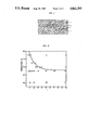
FIG. 2 plots the germanium fraction, x, in a Gex Si1-x layer horizontally versus the substrate growth temperature in units the degrees C. vertically and defines conditions for smooth growth;
FIG. 3 plots the germanium fraction in a Gex Si1-x layer horizontally in units of x versus the tetragonal distortion εt vertically; and
FIG. 4 plots the germanium concentration in units of x in a Gex Si1-x layer horizontally versus the critical thickness in units of Angstroms vertically and defines conditions for defect-free growth.
DETAILED DESCRIPTION
The Gex Si1-x layers are grown by molecular beam epitaxy on substrates, i.e., wafers, that comprise Si or Ge. The conductivity type of the wafer is not critical. For example, both n- and p-type Czochralski silicon wafers may be used. Our invention will be described by reference to growth on Si wafers that had a (100) substrate orientation and resistivities between 0.1 and 10.0 Ω-cm. Other orientations and resistivities may be used.
Prior to loading into the growth chamber, the wafers were precleaned by a series of degreasing, reducing and oxidizing solutions. The precleaned wafers were loaded into the molecular beam epitaxy apparatus for further cleaning. Details of the apparatus are known to those in the art and are described in the Journal of Vacuum Science Technology, 20, pp. 137-142, 1982. The apparatus will comprise both Ge and Si sources as well as sources for appropriate n- and p-type dopants. The cleaning step within the growth chamber is critical as it provides the clean surface needed for epitaxial growth. The clean surface, it is hypothesized, together with the high vacuum, makes it difficult for dislocations to form even though they may be energetically favored over dislocation-free strained layer growth. The wafers are cleaned by, for example, an argon ion sputtering followed by an anneal. The wafers may also be cleaned by heating. The wafer should be of high quality and have a relatively low, less than approximately 100/cm2, dislocation density.
A pure silicon layer is then typically deposited to provide a reproducible initial growth condition. This layer should have a quality that is comparable to that of the substrate. The shutter over the germanium source is then opened and growth of a Gex Si1-x layer begins. All layers are grown at a pressure of 5×10⁻⁸ Torr or less to minimize the presence of impurities that might facilitate dislocation formation. The initial system pressure is approximately 2×10⁻¹⁰ Torr, and the pressure rises during deposition. The background pressure, which is due almost entirely to hydrogen and helium, rises to a value between 5 and 50×10-9 Torr. The deposition sources, i.e., the Ge and Si sources, are commercial electron beam evaporators, and the fluxes are separately sensed and controlled to yield an alloy deposition rate of approximately 5 Angstroms per second. The substrate temperature selection will be discussed later. After the desired Gex Si1-x layer or layers have been grown, a second Si layer is typically also grown.
A cross-sectional view of a structure grown according to the method of this invention is shown in FIG. 1. For reasons of clarity and ease of explanation, the elements of the structure are not drawn to scale. The structure comprises silicon substrate 1, first silicon layer 3, alloy layer 5 comprising Gex Si1-x, x greater than 0.0 and less than or equal to 1.0, and second silicon layer 7. It should be understood that layer 5 may comprise a plurality of Gex Si1-x layers. For example, the layers may have different values of x, or they may be interleaved with a plurality of Si layers. It is also to be understood that the substrate, as well as layers 3 and 7, may comprise Ge. If a Ge substrate is used, x is greater than or equal to 0.0 and less than 1.0.
At a given growth temperature, the alloy films grew in a smooth, two-dimensional manner as x increased from 0.0 to a critical value, xc. When the critical value of x was exceeded, the films grew as discrete, three-dimensional nuclei. The transition between the two types of growth occurred relatively abruptly between x equal to xc and x approximately equal to xc +0.05. As the value of x was further increased above the critical value, a relatively constant morphology was maintained and the nuclei did not display obvious facets but rather had a drop-like appearance which had been previously observed for silicon deposited by molecular beam epitaxy on sapphire substates. The term "two-dimensional" is used for growth of films of uniform thickness and a flat surface.
FIG. 2 plots the germanium fraction, x, horizontally in a 1000 Angstrom thick Gex Si1-x layer, grown on a Si layer over a Si substrate, versus the substrate growth temperature in degrees C., vertically. For temperatures and germanium fractions below the solid line, two-dimensional growth was obtained while three-dimensional growth, that is, islands, was obtained above the line. The circles indicate rough growth while the numbers are the ychan /yrand ratios which are explained below. It can be seen that for any substrate temperature, epitaxial growth is obtained up to a critical value of xc. Above the critical value, islands are grown. The critical value of x increases as the substrate temperature is lowered and reaches a value of 1.0 for substrate temperatures below 550 degrees C., i.e., at substrate temperatures below 550 degrees C., all compositions grow smoothly. Growth should be at a substrate temperature such that the particles in the molecular beam have mobility such that islands do not grow.
If the increase in xc were due to a reduction in atomic surface mobility, it might be expected that crystal quality would degrade. The crystallinity of the films was investigated by both Rutherford backscattering and channeling. The ratio of the [100] channeling to nonaligned backscattering yields from the germanium was used as a definition of ychan /yrand. It is well known that as crystalline perfection increases, channeling improves and the ratio of ychan /yrand decreases from a value of 100 percent for completely disordered material to a value of approximately 3 percent in a perfect crystalline semiconductor. The numbers in FIG. 2 are the numerical values of ychan /yrand and, as is evident, a high-quality crystalline Gex Si1-x layer is obtained over wide ranges of both compositions and substrate deposition temperatures.
At a substrate temperature of 550 degrees C., all alloy compositions grow smoothly. At both 400 and 550 degree C. substrate temperatures, ychan /yrand values increased sharply between values of x=0.2 and x=0.5 for 1000 Angstrom thick films. In an attempt to understand and explain this increase, Gex Si1-x layers having values of x between 0.1 and 1.0 were examined in cross section by transmission electron microscopy, and it was observed that the alloy dislocation density did not increase linearly with the germanium fraction as might be expected on the basis of lattice mismatch. There was an absence of dislocations in the x=0.1 and x=0.2 films, and the number of dislocations increased only gradually for larger values of x. This shows that the lattice mismatch in the x=0.1 and 0.2 films is accommodated by strain, i.e., the alloy film is compressed laterally to match the silicon lattice constant.
If pseudomorphic or strain accommodated alloy growth is taking place, it would be expected that the quality of the layers would also depend on the film thickness and thinner films would have a lower accumulated strain energy and less of a driving force for dislocation formation. This hypothesis was tested by growing Gex Si1-x layers of various thicknesses embedded between two silicon layers. If an alloy layer were thin enough, the alloy layer should grow without dislocations for values of x≧0.5. It was found that for sufficiently thin alloy dislocations were detected. We found accommodation of misfit through strain through layer thicknesses as great as 2500 Angstroms for values of x=0.2. This is surprisingly as the thicknesses of these layers are substantially greater than would expected from an equilibrium analysis of both strain energy and dislocation formation.
Commensurate film growth yields a film free of dislocations with the misfit absorbed by tetragonal distortion. Ion channeling spectra along off-normal channeling directions showed evidence for the tetragonal distortion as a large dechanneling rate in the substrate with the beam aligned in the film. The off-normal <110> and <111> axes make angles, θ, with respect to the [100] normal that are smaller than for the case of cubic symmetry. The difference, Δθ, is related to the tetragonal distortion, εT by ##EQU1## where b and b are the normal and in-plane lattice constants, respectively.
FIG. 3 plots the germanium fraction horizontally versus the tetragonal distortion vertically. The filled and open symbols represent values obtained by ion channeling and x-ray analysis, respectively. The layer thicknesses are shown for each curve in units of Angstroms. The solid line represents a theoretical dependence based on exact in-plane registry in the epilayer, i.e., b.sub.∥ =a, where a is the silicon lattice constant, from which it can be shown that ##EQU2## where ν is Poisson's ratio and f=(b-a)/a, b is the bulk or relaxed Gex Si1-x lattice constant. As is evident, the points in FIG. 3 depart from the straight line as the Ge concentration increases. Thinner layer can be grown with greater Ge fractions as the misfit is accompanied by increased tetragonal distortion. However, a point is reached at which the distortion cannot accommodate all of the strain, and the straight line can no longer be followed. This represents a critical film thickness, hc, for defect-free growth. The thicknesses, hc, are shown in FIG. 4 for several values of x.
The thicknesses are considerably greater than those predicted by model strain and misfit dislocation energies. This might also be termed a "mechanical stability model." We hypothesize that there are barriers to the nucleation and transport of enough misfit dislocations to significantly relax the tetragonal strain in the commensurate heterostructures.
One possible nucleation barrier may be calculated by considering shear displacements of the epilayer with respect to the substrate. The average interfacial energy at the critical thickness may be estimated as μc2 /4π2 d, where μ is the shear modulus, c the slip distance, and d the interplanar spacing. Equating this to the coherency-strain energy, 2(1+ν)μf2 hc /(1-ν), and taking d=a/4 and c=a/√2, gives the result hc ≈0.014 af-2. This estimate accounts for our observation in the vicinity of x=0.25, where it predicts hc =900 Angstroms, although the dependence in FIG. 3 is faster than f-2. We conclude that the strong interfacial bond is important for a large hc, but is not the entire explanation.
Other structures may be grown. For example, a selectively doped heterostructure transistor having a heavily doped wide bandgap material and a normally undoped alloy may be grown. Free carriers generated in the wider bandgap materials would then fall into the narrower bandgap alloy layers. The alloy layer should exhibit higher mobility because there are no ionized impurities and the alloy material has higher mobility. Also, a thin Si layer may be grown on a Gex Si1-x layer and then oxidized forming a Ge MOSFET. Furthermore, as previously mentioned, the alloy layers may be grown on a Ge substrate.

Claims (12)

What is claimed is:
1. A structure comprising a substrate consisting of material selected from the group consisting of Ge and Si and disposed on said substrate, at least one pseudomorphic layer comprising Gex Si1-x, x greater than 0.0 and less than or equal to 1.0 when said substrate is Si, and x greater than or equal to 0.0 and less than 1.0 when said substrate is Ge, said at least one pseudomorphic layer having a thickness approximately equal to hc where hc is approximately equal to 0.014 af-2, a is the silicon lattice constant and f=(b-a)/a where b is the bulk Gex Si1-x lattice constant.
2. A structure as recited in claim 11 in which said substrate comprises Si.
3. A structure as recited in claim 2 further comprising a layer of Si between said substrate and said Gex Si1-x layer.
4. A structure as recited in claim 3 further comprising a layer of Si on said Gex Si1-x layer.
5. A structure as recited in claim 4 in which at least one of said Si layers is doped.
6. A structure as recited in claim 1 comprising a plurality of Gex Si1-x layers.
7. A structure as recited in claim 6 further comprising a layer of Si on said plurality of Gex Si1-x layers.
8. A structure as recited in claim 7 in which said Si layer is oxidized.
9. A structure as recited in claim 1 in which said substrate comprises Ge.
10. A structure as recited in claim 9 further comprising a layer of Si, said layer contacting said Gex Si1-x layer.
11. A structure as recited in claim 10 in which at least a portion of said Si layer is oxidized.
12. A structure as recited in claim 10 in which said Si layer is oxidized.
US07/057,679 1983-10-28 1987-05-28 Semiconductor heterostructures having Gex Si1-x layers on Si utilizing molecular beam epitaxy Expired - Lifetime US4861393A (en)

Priority Applications (1)

Application Number Priority Date Filing Date Title
US07/057,679 US4861393A (en) 1983-10-28 1987-05-28 Semiconductor heterostructures having Gex Si1-x layers on Si utilizing molecular beam epitaxy

Applications Claiming Priority (3)

Application Number Priority Date Filing Date Title
US06/546,736 US4529455A (en) 1983-10-28 1983-10-28 Method for epitaxially growing Gex Si1-x layers on Si utilizing molecular beam epitaxy
US74992185A 1985-06-28 1985-06-28
US07/057,679 US4861393A (en) 1983-10-28 1987-05-28 Semiconductor heterostructures having Gex Si1-x layers on Si utilizing molecular beam epitaxy

Related Parent Applications (1)

Application Number Title Priority Date Filing Date
US74992185A Continuation 1983-10-28 1985-06-28

Publications (1)

Publication Number Publication Date
US4861393A true US4861393A (en) 1989-08-29

Family

ID=27369306

Family Applications (1)

Application Number Title Priority Date Filing Date
US07/057,679 Expired - Lifetime US4861393A (en) 1983-10-28 1987-05-28 Semiconductor heterostructures having Gex Si1-x layers on Si utilizing molecular beam epitaxy

Country Status (1)

Country Link
US (1) US4861393A (en)

Cited By (18)

* Cited by examiner, † Cited by third party
Publication number Priority date Publication date Assignee Title
US5084411A (en) * 1988-11-29 1992-01-28 Hewlett-Packard Company Semiconductor processing with silicon cap over Si1-x Gex Film
US5218213A (en) * 1991-02-22 1993-06-08 Harris Corporation SOI wafer with sige
US5240876A (en) * 1991-02-22 1993-08-31 Harris Corporation Method of fabricating SOI wafer with SiGe as an etchback film in a BESOI process
US5244749A (en) * 1992-08-03 1993-09-14 At&T Bell Laboratories Article comprising an epitaxial multilayer mirror
US5259918A (en) * 1991-06-12 1993-11-09 International Business Machines Corporation Heteroepitaxial growth of germanium on silicon by UHV/CVD
US5268324A (en) * 1992-05-27 1993-12-07 International Business Machines Corporation Modified silicon CMOS process having selectively deposited Si/SiGe FETS
US5286334A (en) * 1991-10-21 1994-02-15 International Business Machines Corporation Nonselective germanium deposition by UHV/CVD
US5354707A (en) * 1993-03-25 1994-10-11 International Business Machines Corporation Method of making semiconductor quantum dot light emitting/detecting devices
US5461243A (en) * 1993-10-29 1995-10-24 International Business Machines Corporation Substrate for tensilely strained semiconductor
US5462883A (en) * 1991-06-28 1995-10-31 International Business Machines Corporation Method of fabricating defect-free silicon on an insulating substrate
US5500391A (en) * 1994-08-09 1996-03-19 At&T Corp. Method for making a semiconductor device including diffusion control
US5685946A (en) * 1993-08-11 1997-11-11 The United States Of America As Represented By The Administrator Of The National Aeronautics And Space Administration Method of producing buried porous silicon-geramanium layers in monocrystalline silicon lattices
US5891769A (en) * 1997-04-07 1999-04-06 Motorola, Inc. Method for forming a semiconductor device having a heteroepitaxial layer
US6087683A (en) * 1998-07-31 2000-07-11 Lucent Technologies Silicon germanium heterostructure bipolar transistor with indium doped base
US6429098B1 (en) * 1997-12-29 2002-08-06 FRANCE TéLéCOM Process for obtaining a layer of single-crystal germanium or silicon on a substrate of single-crystal silicon or germanium, respectively, and multilayer products obtained
US6674102B2 (en) 2001-01-25 2004-01-06 International Business Machines Corporation Sti pull-down to control SiGe facet growth
RU2407103C1 (en) * 2009-10-26 2010-12-20 Учреждение Российской академии наук ИНСТИТУТ ФИЗИКИ МИКРОСТРУКТУР РАН (ИФМ РАН) Method for growing silicon-germanium heterostructures
US20120003799A1 (en) * 2008-11-20 2012-01-05 Jin-Bum Kim Methods of manufacturing semiconductor devices with Si and SiGe epitaxial layers

Citations (9)

* Cited by examiner, † Cited by third party
Publication number Priority date Publication date Assignee Title
US3102828A (en) * 1959-06-02 1963-09-03 Philips Corp Method of manufacturing semiconductor bodies
US3242018A (en) * 1960-07-01 1966-03-22 Siemens Ag Semiconductor device and method of producing it
US3275906A (en) * 1962-08-20 1966-09-27 Nippon Electric Co Multiple hetero-layer composite semiconductor device
US3309553A (en) * 1963-08-16 1967-03-14 Varian Associates Solid state radiation emitters
US3473978A (en) * 1967-04-24 1969-10-21 Motorola Inc Epitaxial growth of germanium
US3615855A (en) * 1969-04-03 1971-10-26 Gen Motors Corp Radiant energy photovoltalic device
US3984857A (en) * 1973-06-13 1976-10-05 Harris Corporation Heteroepitaxial displays
US3993533A (en) * 1975-04-09 1976-11-23 Carnegie-Mellon University Method for making semiconductors for solar cells
US4357183A (en) * 1980-08-13 1982-11-02 Massachusetts Institute Of Technology Heteroepitaxy of germanium silicon on silicon utilizing alloying control

Patent Citations (9)

* Cited by examiner, † Cited by third party
Publication number Priority date Publication date Assignee Title
US3102828A (en) * 1959-06-02 1963-09-03 Philips Corp Method of manufacturing semiconductor bodies
US3242018A (en) * 1960-07-01 1966-03-22 Siemens Ag Semiconductor device and method of producing it
US3275906A (en) * 1962-08-20 1966-09-27 Nippon Electric Co Multiple hetero-layer composite semiconductor device
US3309553A (en) * 1963-08-16 1967-03-14 Varian Associates Solid state radiation emitters
US3473978A (en) * 1967-04-24 1969-10-21 Motorola Inc Epitaxial growth of germanium
US3615855A (en) * 1969-04-03 1971-10-26 Gen Motors Corp Radiant energy photovoltalic device
US3984857A (en) * 1973-06-13 1976-10-05 Harris Corporation Heteroepitaxial displays
US3993533A (en) * 1975-04-09 1976-11-23 Carnegie-Mellon University Method for making semiconductors for solar cells
US4357183A (en) * 1980-08-13 1982-11-02 Massachusetts Institute Of Technology Heteroepitaxy of germanium silicon on silicon utilizing alloying control

Non-Patent Citations (16)

* Cited by examiner, † Cited by third party
Title
B. Y. Tsaur et al., "Heteroepitaxy of Vacuum-Evaporated Ge Films on Single-Crystal Si", Applied Physics Letters, vol. 38, No. 10, May 15, 1981, pp. 779-781.
B. Y. Tsaur et al., Heteroepitaxy of Vacuum Evaporated Ge Films on Single Crystal Si , Applied Physics Letters, vol. 38, No. 10, May 15, 1981, pp. 779 781. *
E. Kasper et al., "A One-Dimensional SiGe Superlattice Grown by UHV Epitaxy", Applied Physics, vol. 8, 1975, pp. 199-205.
E. Kasper et al., "Elastic Strain and Misfit Dislocation Density in Si0.92 Ge0.08 Films on Silicon Substrates", Thin Solid Films, vol. 44, 1977, pp. 357-370.
E. Kasper et al., A One Dimensional SiGe Superlattice Grown by UHV Epitaxy , Applied Physics, vol. 8, 1975, pp. 199 205. *
E. Kasper et al., Elastic Strain and Misfit Dislocation Density in Si 0.92 Ge 0.08 Films on Silicon Substrates , Thin Solid Films, vol. 44, 1977, pp. 357 370. *
J. C. Bean et al., "Silicon MBE Apparatus of Uniform High-Rate Deposition on Standard Format Wafers", Journal of Vacuum Science Technology, vol. 20, No. 2, Feb. 1982, pp. 137-142.
J. C. Bean et al., Silicon MBE Apparatus of Uniform High Rate Deposition on Standard Format Wafers , Journal of Vacuum Science Technology, vol. 20, No. 2, Feb. 1982, pp. 137 142. *
M. Garozzo et al., "Heteroepitaxial Growth of Ge on <111> Si by Vacuum Evaporation", Applied Physics Letters, vol. 41, No. 11, Dec. 1, 1982, pp. 1070-1072.
M. Garozzo et al., Heteroepitaxial Growth of Ge on 111 Si by Vacuum Evaporation , Applied Physics Letters, vol. 41, No. 11, Dec. 1, 1982, pp. 1070 1072. *
V. N. Vasilevskaja et al., "The Effect of Growth Conditions on the Structural and Electrical Properties of the Si-Ge Heteroepitaxial System", Thin Solid Films, vol. 30, 1975, pp. 91-98.
V. N. Vasilevskaja et al., The Effect of Growth Conditions on the Structural and Electrical Properties of the Si Ge Heteroepitaxial System , Thin Solid Films, vol. 30, 1975, pp. 91 98. *
V. N. Vasilevskaya et al., "Structural Perfection of the Ge-Si and Si-Ge Heteroepitaxial Systems", Thin Solid Films, vol. 22, 1974, pp. 221-229.
V. N. Vasilevskaya et al., "The Structure and Electrical Characteristics of Si/Ge Heterojunctions--I: Imperfections in the Si-Ge Heteroepitaxial System Obtained by Deposition of Germanium from a Molecular Beam", Thin Solid Films, vol. 55, 1978, pp. 229-234.
V. N. Vasilevskaya et al., Structural Perfection of the Ge Si and Si Ge Heteroepitaxial Systems , Thin Solid Films, vol. 22, 1974, pp. 221 229. *
V. N. Vasilevskaya et al., The Structure and Electrical Characteristics of Si/Ge Heterojunctions I: Imperfections in the Si Ge Heteroepitaxial System Obtained by Deposition of Germanium from a Molecular Beam , Thin Solid Films, vol. 55, 1978, pp. 229 234. *

Cited By (24)

* Cited by examiner, † Cited by third party
Publication number Priority date Publication date Assignee Title
US5084411A (en) * 1988-11-29 1992-01-28 Hewlett-Packard Company Semiconductor processing with silicon cap over Si1-x Gex Film
US5218213A (en) * 1991-02-22 1993-06-08 Harris Corporation SOI wafer with sige
US5240876A (en) * 1991-02-22 1993-08-31 Harris Corporation Method of fabricating SOI wafer with SiGe as an etchback film in a BESOI process
US5259918A (en) * 1991-06-12 1993-11-09 International Business Machines Corporation Heteroepitaxial growth of germanium on silicon by UHV/CVD
US5462883A (en) * 1991-06-28 1995-10-31 International Business Machines Corporation Method of fabricating defect-free silicon on an insulating substrate
US5540785A (en) * 1991-06-28 1996-07-30 International Business Machines Corporation Fabrication of defect free silicon on an insulating substrate
US5286334A (en) * 1991-10-21 1994-02-15 International Business Machines Corporation Nonselective germanium deposition by UHV/CVD
US5268324A (en) * 1992-05-27 1993-12-07 International Business Machines Corporation Modified silicon CMOS process having selectively deposited Si/SiGe FETS
EP0582407A3 (en) * 1992-08-03 1997-03-12 American Telephone & Telegraph Article comprising an epitaxial multilayer mirror
US5244749A (en) * 1992-08-03 1993-09-14 At&T Bell Laboratories Article comprising an epitaxial multilayer mirror
US5354707A (en) * 1993-03-25 1994-10-11 International Business Machines Corporation Method of making semiconductor quantum dot light emitting/detecting devices
US5685946A (en) * 1993-08-11 1997-11-11 The United States Of America As Represented By The Administrator Of The National Aeronautics And Space Administration Method of producing buried porous silicon-geramanium layers in monocrystalline silicon lattices
US5757024A (en) * 1993-08-11 1998-05-26 The United States Of America As Represented By The Administrator Of The National Aeronautics And Space Administration Buried porous silicon-germanium layers in monocrystalline silicon lattices
US5461243A (en) * 1993-10-29 1995-10-24 International Business Machines Corporation Substrate for tensilely strained semiconductor
US5500391A (en) * 1994-08-09 1996-03-19 At&T Corp. Method for making a semiconductor device including diffusion control
US5891769A (en) * 1997-04-07 1999-04-06 Motorola, Inc. Method for forming a semiconductor device having a heteroepitaxial layer
US6429098B1 (en) * 1997-12-29 2002-08-06 FRANCE TéLéCOM Process for obtaining a layer of single-crystal germanium or silicon on a substrate of single-crystal silicon or germanium, respectively, and multilayer products obtained
US6087683A (en) * 1998-07-31 2000-07-11 Lucent Technologies Silicon germanium heterostructure bipolar transistor with indium doped base
US6674102B2 (en) 2001-01-25 2004-01-06 International Business Machines Corporation Sti pull-down to control SiGe facet growth
US20040063273A1 (en) * 2001-01-25 2004-04-01 International Business Machines Corporation Sti pull-down to control SiGe facet growth
US6936509B2 (en) 2001-01-25 2005-08-30 International Business Machines Corporation STI pull-down to control SiGe facet growth
US20120003799A1 (en) * 2008-11-20 2012-01-05 Jin-Bum Kim Methods of manufacturing semiconductor devices with Si and SiGe epitaxial layers
US8324043B2 (en) * 2008-11-20 2012-12-04 Samsung Electronics Co., Ltd. Methods of manufacturing semiconductor devices with Si and SiGe epitaxial layers
RU2407103C1 (en) * 2009-10-26 2010-12-20 Учреждение Российской академии наук ИНСТИТУТ ФИЗИКИ МИКРОСТРУКТУР РАН (ИФМ РАН) Method for growing silicon-germanium heterostructures

Similar Documents

Publication Publication Date Title
US4529455A (en) Method for epitaxially growing Gex Si1-x layers on Si utilizing molecular beam epitaxy
US4861393A (en) Semiconductor heterostructures having Gex Si1-x layers on Si utilizing molecular beam epitaxy
Bean et al. Pseudomorphic growth of Ge x Si1− x on silicon by molecular beam epitaxy
EP0353423B1 (en) Unstrained defect-free epitaxial mismatched heterostructures and method of fabrication
US8029905B2 (en) GeSiSn-based compounds, templates, and semiconductor structures
US5256550A (en) Fabricating a semiconductor device with strained Si1-x Gex layer
US7323764B2 (en) Buffer structure for modifying a silicon substrate
EP0279989B1 (en) Semiconductor heterostructure having a compositionally varying region comprising SnSi
US4960728A (en) Homogenization anneal of II-VI compounds
US5084411A (en) Semiconductor processing with silicon cap over Si1-x Gex Film
US6594293B1 (en) Relaxed InxGa1-xAs layers integrated with Si
Yano et al. Heteroepitaxial InSb films grown by molecular beam epitaxy
US4948751A (en) Moelcular beam epitaxy for selective epitaxial growth of III - V compound semiconductor
EP0332329B1 (en) Method for making a semiconductor substrate including a strained layer superlattice structure
US6589335B2 (en) Relaxed InxGa1-xAs layers integrated with Si
Herman Silicon‐based heterostructures: strained‐layer growth by molecular beam epitaxy
Wakahara et al. Surfactant effects of Sn on SiGeSi heteroepitaxy by molecular beam epitaxy
JP3169057B2 (en) Method for growing compound semiconductor layer
Kobayashi et al. Molecular beam epitaxy of CdS self-assembled quantum dots on ZnSe
Olsen et al. Growth Effects in the Heteroepitaxy of III–V Compounds
Morishita et al. Facet formation observed in mombe of GaAs on a patterned substrate
Hausler et al. Properties of graded Inx0< or= x< or= 0.5 Ga1-xAs layers grown by molecular beam epitaxy
Lubnow et al. The influence of a hydride preflow on the crystalline quality of InP grown on exactly oriented (100) Si
Itoh et al. The effect of V/III ratio on the initial layer of GaAs on Si
Horikoshi et al. Application of migration-enhanced epitaxy to novel semiconductor structures

Legal Events

Date Code Title Description
STCF Information on status: patent grant

Free format text: PATENTED CASE

FEPP Fee payment procedure

Free format text: PAYOR NUMBER ASSIGNED (ORIGINAL EVENT CODE: ASPN); ENTITY STATUS OF PATENT OWNER: LARGE ENTITY

FPAY Fee payment

Year of fee payment: 4

FEPP Fee payment procedure

Free format text: PAYER NUMBER DE-ASSIGNED (ORIGINAL EVENT CODE: RMPN); ENTITY STATUS OF PATENT OWNER: LARGE ENTITY

Free format text: PAYOR NUMBER ASSIGNED (ORIGINAL EVENT CODE: ASPN); ENTITY STATUS OF PATENT OWNER: LARGE ENTITY

FPAY Fee payment

Year of fee payment: 8

FEPP Fee payment procedure

Free format text: PAYER NUMBER DE-ASSIGNED (ORIGINAL EVENT CODE: RMPN); ENTITY STATUS OF PATENT OWNER: LARGE ENTITY

Free format text: PAYOR NUMBER ASSIGNED (ORIGINAL EVENT CODE: ASPN); ENTITY STATUS OF PATENT OWNER: LARGE ENTITY

FPAY Fee payment

Year of fee payment: 12

AS Assignment

Owner name: AGERE SYSTEMS INC., PENNSYLVANIA

Free format text: ASSIGNMENT OF ASSIGNORS INTEREST;ASSIGNORS:AT&T CORP.;LUCENT TECHNOLOGIES INC.;REEL/FRAME:016301/0651;SIGNING DATES FROM 19960329 TO 20010130