US4853756A - Projection exposure apparatus - Google Patents
Projection exposure apparatus Download PDFInfo
- Publication number
- US4853756A US4853756A US07/147,796 US14779688A US4853756A US 4853756 A US4853756 A US 4853756A US 14779688 A US14779688 A US 14779688A US 4853756 A US4853756 A US 4853756A
- Authority
- US
- United States
- Prior art keywords
- light
- bandpass
- path
- illumination system
- filter
- Prior art date
- Legal status (The legal status is an assumption and is not a legal conclusion. Google has not performed a legal analysis and makes no representation as to the accuracy of the status listed.)
- Expired - Lifetime
Links
Images


Classifications
-
- G—PHYSICS
- G03—PHOTOGRAPHY; CINEMATOGRAPHY; ANALOGOUS TECHNIQUES USING WAVES OTHER THAN OPTICAL WAVES; ELECTROGRAPHY; HOLOGRAPHY
- G03F—PHOTOMECHANICAL PRODUCTION OF TEXTURED OR PATTERNED SURFACES, e.g. FOR PRINTING, FOR PROCESSING OF SEMICONDUCTOR DEVICES; MATERIALS THEREFOR; ORIGINALS THEREFOR; APPARATUS SPECIALLY ADAPTED THEREFOR
- G03F7/00—Photomechanical, e.g. photolithographic, production of textured or patterned surfaces, e.g. printing surfaces; Materials therefor, e.g. comprising photoresists; Apparatus specially adapted therefor
- G03F7/70—Microphotolithographic exposure; Apparatus therefor
- G03F7/70483—Information management; Active and passive control; Testing; Wafer monitoring, e.g. pattern monitoring
- G03F7/7055—Exposure light control in all parts of the microlithographic apparatus, e.g. pulse length control or light interruption
- G03F7/70575—Wavelength control, e.g. control of bandwidth, multiple wavelength, selection of wavelength or matching of optical components to wavelength
Definitions
- This invention relates to a projection exposure apparatus and, more particularly, to a projection exposure apparatus called a "stepper" having a projection lens system by which a circuit pattern of a reticle or otherwise is projected upon a wafer.
- the degree of integration of devices such as semiconductor microcircuits which are to be manufactured by use of exposure apparatuses has been rapidly increased. For example, at present, one-megabit memory devices can be manufactured practicably. Also, it is expected that four-megabit memory devices will be practicably manufactured in the near future.
- exposure apparatuses for use in the manufacture of microcircuits should have high performance.
- the apparatus should have superior alignment capability for precisely superimposing different patterns in plural pattern printing processes. Also, it should have a superior processing capability that allows execution of the wafer printing procedure with high throughput. Further, the apparatus should have excellent resolution that permits printing of fine patterns having a linewidth not greater than 0.8 micron.
- the projection exposure apparatus includes a projection lens system having been corrected, precisely, for various optical aberrations in order to assure improved pattern transfer or printing performance. However, it is not difficult to completely avoid the optical aberrations, particularly the chromatic aberration.
- the currently available steppers prevalently use, as for the photoprinting light, g-line rays having a wavelength (central wavelength) 436 nm.
- the light of g-line has a bandwidth which is, as shown in FIG. 2, 10 nm (half width) at the peak 436 nm.
- the bandwidth narrowing is made to diminish the effect of the chromatic aberration of the projection optical system, thereby to assure high resolution performance.
- the bandwidth narrowing is not always advantageous. Namely, for the light having the same peak intensity (see FIG. 4), the band narrowing results in cutting or intercepting such quantity of light as corresponding to the hatched area in FIG. 4. This innevitably causes substantial reduction in the quantity of light that can be used for the photoprinting. This leads to a problem that, in a case where a pattern having a relatively wide line-width is going to be photoprinted in some of various printing procedures for the manufacture of the same microcircuit, the printing of such relatively wide line-width pattern has to be executed with an insufficient quantity of light.
- a projection exposure apparatus which includes a projection lens system for projecting a pattern of an original upon a workpiece, an illumination optical system for illuminating the original with a light having a predetermined central wavelength, and a bandwidth changing arrangement effective to change the bandwidth of the light irradiating the original.
- an illumination optical system of a projection exposure apparatus has a plurality of optical elements having different bandpass characteristics. These optical elements are selectively and retractively inserted into a path of the light from a light source such as an Hg lamp or otherwise.
- the optical elements are interchangeably used in the illumination optical system so as to change the bandwidth of the light used for the photoprinting.
- This allows that, for the printing of such a pattern having a relatively wide linewidth, the printing is carried out with a large quantity of light having a relatively broad bandwidth. Thus, high throughput is ensured.
- light having a very narrow bandwidth is used to thereby minimize the effect of the chromatic aberration of the projection lens system.
- high-resolution printing is attainable. In this manner, the wafer processing capability and the resolution characteristics of the exposure apparatus are made adjustable as desired.
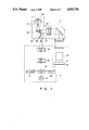
- FIG. 1 is a schematic and diagrammatic view of a projection exposure apparatus according to one embodiment of the present invention.
- FIGS. 2 and 3 are graphs, respectively, showing the spectral characteristics of a g-line light having a half width 10 nm and a g-line light having a half width 5 nm.
- FIG. 4 is a graph schematically showing the difference in the quantity, for the light shown in FIG. 2 and the light shown in FIG. 3.
- FIG. 1 there is shown a projection exposure apparatus according to one embodiment of the present invention, which apparatus includes an illumination optical system and a control system.
- Denoted at 1 in FIG. 1 is a photomask having a circuit pattern formed thereon.
- Denoted generally at 3 is an illumination optical system which includes at least two different bandpass filters and a filter changing arrangement.
- denoted generally at 2 is a control system for controlling the changing of the filters.
- Light emitted from an Hg lamp 31 included in the illumination optical system 3 is corrected by a parabolic mirror 32 and then is deflected by a reflection mirror 33.
- the light from the mirror 33 passes through a sharp-cut filter 34 which is effective to cut the wavelengths in the "heat wave” region.
- the light passes through a bandpass filter 35, whereby the bandwidth of the light to be used for the photoprinting is determined.
- the filter 35 After passing the filter 35, the light is directed by a condenser lens and a reflection mirror to the photomask 1 (which may of course be a reticle), thereby to irradiate the same as the "photoprinting light".
- Denoted at 40 in FIG. 1 is a projection lens system which comprises a plurality of lens elements.
- the projection lens system 40 has been corrected for the various optical aberrations, with reference to a particular design wavelength (central wavelength) which is that of the g-line light in this embodiment.
- the projection lens system has an imaging magnification in a range of 1/5 to 1/10.
- Denoted at 41 is a wafer having a surface which is coated with a suitable resist material.
- the wafer 41 is placed on a wafer stage 42 which is movable in suitable directions.
- the circuit pattern of the photomask 1 as illuminated by the light from the illumination optical system 3 is projected by the projection lens system 40 upon the wafer 41 in a reduced scale. By this, the circuit pattern of the photomask 1 is transferred onto or photoprinted on the wafer 41.
- the light emitted from the lamp 31 contains plural line spectrums such as g-line, h-line (405 nm), e-line (546 nm) and otherwise.
- the sharp-cut filter 34 and the bandpass filter 35 (or 36) are used for the wavelength selection, such that light of a single line spectrum having a central wavelength corresponding to that of the g-line, is extracted. Further, the extracted g-line light has a bandwidth which is determined by the bandpass characteristics of the bandpass filter 35 or 36.
- the bandpass filters 35 and 36 have been designed so that the light passed through the bandpass filter 35 (hereinafter such light will be referred to also as a "first photoprinting light”) has the spectral characteristics such as shown in FIG. 2 while, on the other hand, the light passed through the bandpass filter 36 (hereinafter such light will be referred to also as a “second photoprinting light”) has the spectral characteristics such as shown in FIG. 3.
- Each of the bandpass filters 35 and 36 may be provided by a multi-layered interference thin film filter such as disclosed in the aforementioned U.S. patent application Ser. No. 813,226 or it may be formed by a wavelength selecting element such as an etalon or otherwise.
- the bandpass filter 35 is used for the photoprinting of such a pattern having a relatively wide linewidth.
- the bandpass filter 36 is used for the photoprinting of such a pattern having a narrow linewidth. Accordingly, for the photoprinting of a pattern having a relatively large linewidth (e.g. 1.5-2.0 microns), the throughput of the exposure apparatus can be increased (e.g. 1.5-2 times higher).
- the bandpass filters 35 and 36 are interchanged in accordance with the photomask 1 used (namely, the linewidth of the circuit pattern).
- the bandpass filters 35 and 36 are fixedly mounted to a common support member which is coupled to a rotational shaft of an actuator 37. By rotating the support member, the bandpass filters 35 and 36 are interchanged.
- an operator designates, by typing an input keyboard 21 of the control system 2, a particular bandwidth to be selected or a particular filter having bandpass characteristics corresponding to the bandwidth to be selected.
- the information concerning the bandwidth to be used is stored into a memory 22 by way of a console CPU (central processing unit) 24.
- a console CPU central processing unit
- Such information is displayed on a CRT (cathode ray tube) 23.
- the information concerning the bandwidth stored in the memory 22 is transmitted to a control CPU 25, wherein the information signal is converted into an instruction voltage corresponding to the selected bandwidth.
- the instruction voltage is applied to a driving circuit 26, such that the actuator 37 is driven to replace a bandpass filter (e.g. 35) positioned in the path of the light from the lap 31 by another bandpass filter (e.g. 36).
- the actuator 37 may comprise a DC motor, a pulse motor, an air cylinder or otherwise.
- Position detecting sensor 38 is provided to detect the position of the extracted bandpass filter (which is the filter 35 in this case) and, therefore, the position of the newly introduced bandpass filter (which is the filter 36 in this example). When the selected bandpass filter is placed at a correct position and if this is confirmed by the sensor 38, the bandwidth changing operation is completed.
- the bandpass filters 35 and 36 provided in the illumination optical system can be selected as desired.
- the bandpass filters 35 and 36 are selected as desired to thereby change the bandwidth of the photoprinting light having a central wavelength equal to that of the g-line.
- the bandwidth changing i.g. changing the wavelength range
- the bandpass filters 35 and 36 may be designed and manufactured so that the bandpass filter 35 is effective to extract a particular line spectrum together with a continuous spectrum adjacent to the particular line spectrum while the bandpass filter 36 is effective to cut the continuous spectrum with the result that only the particular line spectrum is extracted. Details of the relation between the line spectrum and the continuous spectrum are disclosed in the aforementioned U.S. patent application Ser. No. 813,226.
- Each of the bandpass filters 35 and 36 when it is introduced, is preferably disposed at such position at which the light from the light source such as the lamp 31 advances as a parallel light (i.e. the position at which the chief ray advances in parallel to the optical axis of the illumination optical system). With this arrangement, the wavelength selecting characteristics of the filter can function correctly, for the light from the light source.
- bandpass filters are used as the wavelength variably-selecting optical means which is effective to change the bandwidth
- optical means may comprise a combination of a sharp-cut filter and an interference filter (such as an etalon or otherwise) or a bandpass filter formed by a multilayered interference thin film.
- the wavelength selecting optical means is provided by a combination of a sharp-cut filter and an interference filter or two or more bandpass filters, the bandwidth may of course be changed by changing one or more filters or by changing the combination of these filters.
- the present invention is effectively applicable also to a projection exposure apparatus having a laser such as an excimer laser as the light source.
- a laser such as an excimer laser as the light source.
- the bandwidth (wavelength range) of the laser beam can be variably narrowed, as desired, by interchanging different wavelength selecting elements such as etalons, diffraction gratings or otherwise having different band-narrowing characteristics.
- the printing of a pattern having a relatively large linewidth can be executed with a large quantity of light, thus ensuring high throughput.
- the effect of the chromatic aberration of a projection lens system can be minimized with the result that high-resolution pattern printing is attainable. Therefore, the exposure apparatus can be operated in a most suitable and efficient manner, which is best suited to the characteristics of the pattern to be printed and to the desire of the operator who handles the apparatus.
Abstract
Description
Claims (8)
Applications Claiming Priority (2)
| Application Number | Priority Date | Filing Date | Title |
|---|---|---|---|
| JP62-15999 | 1987-01-28 | ||
| JP62015999A JPS63185023A (en) | 1987-01-28 | 1987-01-28 | Aligner |
Publications (1)
| Publication Number | Publication Date |
|---|---|
| US4853756A true US4853756A (en) | 1989-08-01 |
Family
ID=11904332
Family Applications (1)
| Application Number | Title | Priority Date | Filing Date |
|---|---|---|---|
| US07/147,796 Expired - Lifetime US4853756A (en) | 1987-01-28 | 1988-01-25 | Projection exposure apparatus |
Country Status (2)
| Country | Link |
|---|---|
| US (1) | US4853756A (en) |
| JP (1) | JPS63185023A (en) |
Cited By (22)
| Publication number | Priority date | Publication date | Assignee | Title |
|---|---|---|---|---|
| US4931830A (en) * | 1988-08-12 | 1990-06-05 | Nikon Corporation | Projection exposure apparatus |
| US4937619A (en) * | 1986-08-08 | 1990-06-26 | Hitachi, Ltd. | Projection aligner and exposure method |
| US5303002A (en) * | 1993-03-31 | 1994-04-12 | Intel Corporation | Method and apparatus for enhancing the focus latitude in lithography |
| US5552891A (en) * | 1994-10-31 | 1996-09-03 | International Business Machines Corporation | Automated mask alignment for UV projection expose system |
| US5574492A (en) * | 1992-03-27 | 1996-11-12 | Canon Kabushiki Kaisha | Imaging method and semiconductor device manufacturing method using the same |
| US5610684A (en) * | 1994-02-17 | 1997-03-11 | Nikon Corporation | Projection exposure apparatus |
| US5661547A (en) * | 1990-03-09 | 1997-08-26 | Canon Kabushiki Kaisha | Exposure method and apparatus and device produced thereby in which a stop includes an opening which is variable to substantially compensate for a change in bandwidth of a laser beam |
| US5789734A (en) * | 1993-05-14 | 1998-08-04 | Canon Kabushiki Kaisha | Exposure apparatus that compensates for spherical aberration of an image forming device |
| US5831715A (en) * | 1994-01-27 | 1998-11-03 | Canon Kabushiki Kaisha | Projection exposure apparatus with means to vary spherical aberration |
| US6304317B1 (en) | 1993-07-15 | 2001-10-16 | Nikon Corporation | Projection apparatus and method |
| US6322220B1 (en) | 1994-02-14 | 2001-11-27 | Canon Kabushiki Kaisha | Exposure apparatus and device manufacturing method using the same |
| US20030043356A1 (en) * | 1990-11-15 | 2003-03-06 | Nikon Corporation | Projection exposure apparatus and method |
| US6636293B1 (en) | 1990-08-21 | 2003-10-21 | Nikon Corporation | Exposure method and apparatus having a decreased light intensity distribution |
| US6665050B2 (en) | 1990-11-15 | 2003-12-16 | Nikon Corporation | Projection exposure methods using difracted light with increased intensity portions spaced from the optical axis |
| US6710854B2 (en) | 1991-09-11 | 2004-03-23 | Nikon Corporation | Projection exposure apparatus |
| US20040227919A1 (en) * | 1990-11-15 | 2004-11-18 | Nikon Corporation | Projection exposure apparatus and method |
| US20040233411A1 (en) * | 1990-11-15 | 2004-11-25 | Nikon Corporation | Projection exposure apparatus and method |
| US6842225B1 (en) * | 1999-05-07 | 2005-01-11 | Nikon Corporation | Exposure apparatus, microdevice, photomask, method of exposure, and method of production of device |
| US20050196713A1 (en) * | 1991-03-05 | 2005-09-08 | Minori Noguchi | Exposure apparatus and method |
| US6967710B2 (en) | 1990-11-15 | 2005-11-22 | Nikon Corporation | Projection exposure apparatus and method |
| US20090097008A1 (en) * | 2007-10-09 | 2009-04-16 | Asml Netherlands B.V | Alignment Method and Apparatus, Lithographic Apparatus, Metrology Apparatus and Device Manufacturing Method |
| US7656504B1 (en) | 1990-08-21 | 2010-02-02 | Nikon Corporation | Projection exposure apparatus with luminous flux distribution |
Families Citing this family (1)
| Publication number | Priority date | Publication date | Assignee | Title |
|---|---|---|---|---|
| JP5267539B2 (en) | 2010-11-05 | 2013-08-21 | ダイキン工業株式会社 | Floor-standing indoor unit |
Citations (3)
| Publication number | Priority date | Publication date | Assignee | Title |
|---|---|---|---|---|
| US4351608A (en) * | 1979-11-13 | 1982-09-28 | Ciba-Geigy Ag | Filter head |
| US4653903A (en) * | 1984-01-24 | 1987-03-31 | Canon Kabushiki Kaisha | Exposure apparatus |
| US4789222A (en) * | 1983-03-04 | 1988-12-06 | Canon Kabushiki Kaisha | Illuminating optical system |
-
1987
- 1987-01-28 JP JP62015999A patent/JPS63185023A/en active Pending
-
1988
- 1988-01-25 US US07/147,796 patent/US4853756A/en not_active Expired - Lifetime
Patent Citations (3)
| Publication number | Priority date | Publication date | Assignee | Title |
|---|---|---|---|---|
| US4351608A (en) * | 1979-11-13 | 1982-09-28 | Ciba-Geigy Ag | Filter head |
| US4789222A (en) * | 1983-03-04 | 1988-12-06 | Canon Kabushiki Kaisha | Illuminating optical system |
| US4653903A (en) * | 1984-01-24 | 1987-03-31 | Canon Kabushiki Kaisha | Exposure apparatus |
Cited By (29)
| Publication number | Priority date | Publication date | Assignee | Title |
|---|---|---|---|---|
| US4937619A (en) * | 1986-08-08 | 1990-06-26 | Hitachi, Ltd. | Projection aligner and exposure method |
| US4931830A (en) * | 1988-08-12 | 1990-06-05 | Nikon Corporation | Projection exposure apparatus |
| US5661547A (en) * | 1990-03-09 | 1997-08-26 | Canon Kabushiki Kaisha | Exposure method and apparatus and device produced thereby in which a stop includes an opening which is variable to substantially compensate for a change in bandwidth of a laser beam |
| US7656504B1 (en) | 1990-08-21 | 2010-02-02 | Nikon Corporation | Projection exposure apparatus with luminous flux distribution |
| US6636293B1 (en) | 1990-08-21 | 2003-10-21 | Nikon Corporation | Exposure method and apparatus having a decreased light intensity distribution |
| US6665050B2 (en) | 1990-11-15 | 2003-12-16 | Nikon Corporation | Projection exposure methods using difracted light with increased intensity portions spaced from the optical axis |
| US6710855B2 (en) | 1990-11-15 | 2004-03-23 | Nikon Corporation | Projection exposure apparatus and method |
| US6967710B2 (en) | 1990-11-15 | 2005-11-22 | Nikon Corporation | Projection exposure apparatus and method |
| US6897942B2 (en) | 1990-11-15 | 2005-05-24 | Nikon Corporation | Projection exposure apparatus and method |
| US6885433B2 (en) | 1990-11-15 | 2005-04-26 | Nikon Corporation | Projection exposure apparatus and method |
| US20030043356A1 (en) * | 1990-11-15 | 2003-03-06 | Nikon Corporation | Projection exposure apparatus and method |
| US20040233411A1 (en) * | 1990-11-15 | 2004-11-25 | Nikon Corporation | Projection exposure apparatus and method |
| US20040227919A1 (en) * | 1990-11-15 | 2004-11-18 | Nikon Corporation | Projection exposure apparatus and method |
| US6704092B2 (en) | 1990-11-15 | 2004-03-09 | Nikon Corporation | Projection exposure method and apparatus that produces an intensity distribution on a plane substantially conjugate to a projection optical system pupil plane |
| US7277155B2 (en) * | 1991-03-05 | 2007-10-02 | Renesas Technology Corp. | Exposure apparatus and method |
| US20050196713A1 (en) * | 1991-03-05 | 2005-09-08 | Minori Noguchi | Exposure apparatus and method |
| US6864959B2 (en) | 1991-09-11 | 2005-03-08 | Nikon Corporation | Projection exposure apparatus |
| US6710854B2 (en) | 1991-09-11 | 2004-03-23 | Nikon Corporation | Projection exposure apparatus |
| US5574492A (en) * | 1992-03-27 | 1996-11-12 | Canon Kabushiki Kaisha | Imaging method and semiconductor device manufacturing method using the same |
| US5303002A (en) * | 1993-03-31 | 1994-04-12 | Intel Corporation | Method and apparatus for enhancing the focus latitude in lithography |
| US5789734A (en) * | 1993-05-14 | 1998-08-04 | Canon Kabushiki Kaisha | Exposure apparatus that compensates for spherical aberration of an image forming device |
| US6304317B1 (en) | 1993-07-15 | 2001-10-16 | Nikon Corporation | Projection apparatus and method |
| US5831715A (en) * | 1994-01-27 | 1998-11-03 | Canon Kabushiki Kaisha | Projection exposure apparatus with means to vary spherical aberration |
| US6322220B1 (en) | 1994-02-14 | 2001-11-27 | Canon Kabushiki Kaisha | Exposure apparatus and device manufacturing method using the same |
| US5610684A (en) * | 1994-02-17 | 1997-03-11 | Nikon Corporation | Projection exposure apparatus |
| US5552891A (en) * | 1994-10-31 | 1996-09-03 | International Business Machines Corporation | Automated mask alignment for UV projection expose system |
| US5569570A (en) * | 1994-10-31 | 1996-10-29 | International Business Machines Corporation | Automated mask alignment for UV projection exposure system |
| US6842225B1 (en) * | 1999-05-07 | 2005-01-11 | Nikon Corporation | Exposure apparatus, microdevice, photomask, method of exposure, and method of production of device |
| US20090097008A1 (en) * | 2007-10-09 | 2009-04-16 | Asml Netherlands B.V | Alignment Method and Apparatus, Lithographic Apparatus, Metrology Apparatus and Device Manufacturing Method |
Also Published As
| Publication number | Publication date |
|---|---|
| JPS63185023A (en) | 1988-07-30 |
Similar Documents
| Publication | Publication Date | Title |
|---|---|---|
| US4853756A (en) | Projection exposure apparatus | |
| EP0969327B1 (en) | Multiple exposure apparatus and method | |
| US7126667B2 (en) | Exposure apparatus and method | |
| TW544547B (en) | Exposure method and apparatus | |
| US6934009B2 (en) | Illumination apparatus, illumination-controlling method, exposure apparatus, device fabricating method | |
| JP2004519850A (en) | Method and apparatus for exposing a dual reticle image | |
| US6727976B2 (en) | Exposure apparatus with a pulsed laser | |
| JPH04369209A (en) | Illumination apparatus for exposure use | |
| JP2000021748A (en) | Method of exposure and exposure equipment | |
| JP3391404B2 (en) | Projection exposure method and circuit element manufacturing method | |
| JPH06252021A (en) | Projection exposure method and device therefor | |
| JP3084760B2 (en) | Exposure method and exposure apparatus | |
| JP2001237183A (en) | Microlithography projection apparatus | |
| US5621500A (en) | Method and apparatus for projection exposure | |
| US7359033B2 (en) | Exposure method and apparatus | |
| US20070211231A1 (en) | Exposure apparatus and device manufacturing method | |
| JPH07122478A (en) | Pattern projection method | |
| JP2004207709A (en) | Exposure method and device | |
| JP2000311853A (en) | Aligning method, fabrication of device using that method, and aligner | |
| JP2692660B2 (en) | Projection exposure apparatus and projection exposure method | |
| JPH0644549B2 (en) | Projection exposure method and apparatus | |
| JPH1050590A (en) | Projection aligner | |
| JP7446068B2 (en) | Exposure apparatus and article manufacturing method | |
| JPH06318542A (en) | Projection aligner | |
| JP3279311B2 (en) | Projection exposure method and apparatus, and circuit element manufacturing method using the method |
Legal Events
| Date | Code | Title | Description |
|---|---|---|---|
| AS | Assignment |
Owner name: CANON KABUSHIKI KAISHA, 3-30-2 SHIMOMARUKO, OHTA-K Free format text: ASSIGNMENT OF ASSIGNORS INTEREST.;ASSIGNOR:MATSUKI, TOSHIO;REEL/FRAME:004840/0201 Effective date: 19880118 Owner name: CANON KABUSHIKI KAISHA, A CORP. OF JAPAN,JAPAN Free format text: ASSIGNMENT OF ASSIGNORS INTEREST;ASSIGNOR:MATSUKI, TOSHIO;REEL/FRAME:004840/0201 Effective date: 19880118 |
|
| STCF | Information on status: patent grant |
Free format text: PATENTED CASE |
|
| CC | Certificate of correction | ||
| FPAY | Fee payment |
Year of fee payment: 4 |
|
| FPAY | Fee payment |
Year of fee payment: 8 |
|
| FEPP | Fee payment procedure |
Free format text: PAYOR NUMBER ASSIGNED (ORIGINAL EVENT CODE: ASPN); ENTITY STATUS OF PATENT OWNER: LARGE ENTITY Free format text: PAYER NUMBER DE-ASSIGNED (ORIGINAL EVENT CODE: RMPN); ENTITY STATUS OF PATENT OWNER: LARGE ENTITY |
|
| FPAY | Fee payment |
Year of fee payment: 12 |