US4734921A - Fully programmable linear feedback shift register - Google Patents
Fully programmable linear feedback shift register Download PDFInfo
- Publication number
- US4734921A US4734921A US06/934,588 US93458886A US4734921A US 4734921 A US4734921 A US 4734921A US 93458886 A US93458886 A US 93458886A US 4734921 A US4734921 A US 4734921A
- Authority
- US
- United States
- Prior art keywords
- flip
- flops
- data
- shift register
- input
- Prior art date
- Legal status (The legal status is an assumption and is not a legal conclusion. Google has not performed a legal analysis and makes no representation as to the accuracy of the status listed.)
- Expired - Fee Related
Links
Images


Classifications
-
- G—PHYSICS
- G01—MEASURING; TESTING
- G01R—MEASURING ELECTRIC VARIABLES; MEASURING MAGNETIC VARIABLES
- G01R31/00—Arrangements for testing electric properties; Arrangements for locating electric faults; Arrangements for electrical testing characterised by what is being tested not provided for elsewhere
- G01R31/28—Testing of electronic circuits, e.g. by signal tracer
- G01R31/317—Testing of digital circuits
- G01R31/3181—Functional testing
- G01R31/31813—Test pattern generators
-
- G—PHYSICS
- G06—COMPUTING OR CALCULATING; COUNTING
- G06F—ELECTRIC DIGITAL DATA PROCESSING
- G06F7/00—Methods or arrangements for processing data by operating upon the order or content of the data handled
- G06F7/58—Random or pseudo-random number generators
- G06F7/582—Pseudo-random number generators
- G06F7/584—Pseudo-random number generators using finite field arithmetic, e.g. using a linear feedback shift register
-
- G—PHYSICS
- G11—INFORMATION STORAGE
- G11C—STATIC STORES
- G11C19/00—Digital stores in which the information is moved stepwise, e.g. shift registers
Definitions
- the present invention relates to shift registers and more particularly to a fully programmable linear feedback shift register.
- Linear feedback shift registers which use a number of flip-flops for circulating information by means of a sequence of bits are known. It is further known that such shift registers may be used for error coding and pseudo-random number generation. However, for each of these applications, a differently configured shift register needs to be used. Further, the hardware for the shift registers can get to be quite extensive, where repeatability is desired for a great number of times.
- the present invention achieves a successful resolution of the aforesaid problems by presenting a linear feedback shift register which is fully programmable, thereby eliminating the need to have a particular configured shift register for a specific function.
- the flip-flops and control logic circuits in the present invention shift register are configured in such a way that the register can be used, aside from the above-mentioned functions of a conventional linear feedback shift register, for encoding and encryption of information.
- the present invention shift register utilizes a plurality of flip-flop stages each with its own control logic circuits. Each flip-flop stage is identical; and consequently, the shift register can be programmed for different lengths, as the number of flip-flops need not remain static. The output of any one of the flip-flops can be fed, via a feedback circuit, to the beginning stage of the shift register, thereby providing a myriad of different length shift registers.
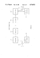
- FIG. 1 is an illustration of how the present invention shift register can be used in an overall system
- FIG. 2 (including 2A and 2B) is a schematic representing the detailed digital realization of the present invention shift register
- FIG. 3 (including 3A and 3B) is a schematic diagram showing the cascading of a number of FIG. 2 shift registers.
- a crypto-communication system wherein a present invention shift register is incorporated.
- a fully programmable linear feedback shift register 2A hereinafter to be referred to as FPLFSR 2A
- FPLFSR 2A is connected to a data source 4A, a micro-processor 6A and a modem 8A.
- Data which is to be transmitted to a corresponding system is sent from data source 4A to FPLFSR 2A, wherein this data is encoded, before being sent to the corresponding system.
- FPLFSR 2A is controlled by micro-processor 6A.
- modem 8B Upon receiving the encoded data, modem 8B transmits the encoded data to FPLFSR 2B, wherein the encoded data is unscrambled. It should be noted that both sets of transmitting and receiving components are identical and that the equations used for scrambling and unscrambling the data are the same.
- FIG. 2 wherein a schematic drawing of the present invention shift register is shown.
- the shift register is not limited to such a number, for an indefinite number of flip-flops and/or a multiple number of basic block shift registers can be cascaded to form shift registers having different numbers of flip-flops.
- FPLFSR 2 has four identical flip-flops FFA, FFB, FFC, and FFD. These flip-flops, for this example, are shown to be D-type flip-flops. Each of the flip-flops is associated to a number of logic gates, which are also identical.
- stage B associated with flip-flop FFB are three AND gates 12B, 18B and 14B, exclusive OR gate 16B and an OR gate 20B. Except for the first stage, that is, stage A, all of the logic gates in remaining stages B, C and D are similarly connected to their respective flip-flops. Thus, it is sufficient that only one of these stages is discussed.
- AND gate 14B has four inputs. The first input comes from the F -- P line (Feedback/Parallel Load Control line). This line primes flip-flops FFA to FFD of the FPLFSR for parallel loading from lines FCn -- PLn--to be discussed below--when the logic state thereon is low; for normal operation, the logic state of F -- P remains high.
- F -- P line Feeback/Parallel Load Control line
- FC1 -- PL1 line (Feedback Control/Parallel Load line).
- FCn -- PLn lines Data fed from these lines are to be used either for parallel loading of a polynomial equation or for feedback control of the flip-flops.
- a third input into AND gate 14B comes from the output of exclusive OR gate 26.
- the inputs and function of exclusive OR gate 26 will be described in greater detail, infra.
- the last input going into AND gate 14B comes from an FFE1 line (Flip-flop Enable line), which is but one of three identical lines.
- AND gate 12B, along with AND gates 12C and 12D, has three inputs. The first input for AND gate 12B comes from line F -- P, which was described earlier. A second input comes from line FFE1. The last input comes from the output of flip-flop FFA of Stage A.
- AND gate 18B like AND gates 18C and 18D, also has three inputs: the first input is fed from line FFE1; the second input is connected to line FC1 -- PL1; and the last input is connected to a line having a logic state opposite to that of line F -- P.
- flip-flop B The output of flip-flop B is fed to the input of AND gate 12C of flip-flop Stage C. Likewise, the output of flip-flop Stage C is sent to the input of AND gate 12D, thereby completing a series of cascaded flip-flop stages.
- the flip-flops are controlled by the timing pulses from the CLK line. Also, each of the flip-flops gets its power from VCC.
- flip-flop Stage A There are differences between the connections of the logic gates in flip-flop Stage A, when compared to the remaining flip-flop stages of the FIG. 2 embodiment.
- AND gate 12A there are only two inputs. The first input is fed from line F -- P while the second input is fed from line QIN, which is the serial data input for the first stage of the shift register; alternatively, the second input of AND gate 12A may be fed the cascaded output from the last flip-flop of a previous shift register.
- Another difference in flip-flop Stage A is that there are only two inputs to AND gate 18A. The first input is fed from line FC0 -- PL0 while the second input is fed from line F -- P', which has a logic state opposite to that of line F -- P. As shown, the change of the logic state is due to the insertion of NOT gate 22 between line F -- P and the inputs to respective AND gates 18A, 18B, 18C and 18D.
- the outputs of the respective flip-flop stages are cascaded from one stage to the next. Also, these outputs, i.e., Q0, Q1, Q2 and Q3, are respectively connected to AND gates 30A, 30B, 30C and 30D.
- AND gate 30D a second input is connected to line FFE3.
- the output of line FFE3 is converted into the opposite logic state by NOT gate 28C and fed as an input to AND gate 30C, which has an input fed from line FFE2.
- the logic state of line FFE2 is converted to an opposed sense by NOT gate 28B and fed to AND gate 30B, which also has as a third input line FFE1.
- the logic state of line FFE1 is inverted by NOT gate 28A and fed as an input to AND gate 30A.
- Each of the outputs of AND gates 30A to 30D is input to OR gate 32, which has as its output signal NEWOUT.
- NEWOUT represents the output of the last flip-flop stage used in the shift register.
- the outputs of the respective flip-flops are also connected as inputs to OR gate 34, thereby generating therefrom a CRC -- OUT output (Cyclic Redundancy Check Output). This output will be high when any of the flip-flop outputs is high in the basic shift register building block of FIG. 2.
- Output NEWOUT is fed to an input of AND gate 24, which also has an input signal from a F -- E line (Feedback Enable Line).
- the output from AND gate 24 is fed as an input to exclusive OR gate 26.
- An additional input to exclusive OR gate 26 is fed from line DATAIN.
- the output from exclusive OR gate 26 is fed simultaneously to the inputs of respective AND gates 14A, 14B, 14C and 14D.
- the same output is further routed to a CAS -- EN line (Cascade Enable Line).
- the CAS -- EN line may be used to cascade the FIG. 2 basic block shift register to an additional similar basic shift register block via the latter's DATAIN line.
- a polynomial equation has to be first input into the respective flip-flops.
- This equation determines the number of flip-flops to be used, as well as the number of cycles before an initial message will repeat. For example, were a polynomial equation of x 20 +x 3 +1 used, one would be able to ascertain from this equation that 20 flip-flops are to be used for the particular shift register. In the event that a basic building block shift register, for example, that shown in FIG. 2, is available, then five of these basic blocks would be cascaded together, per FIG. 4, so that there is a total of 20 flip-flops. In other words, the order of the polynomial equation signifies the number of flip-flops to be used in that particular programmable linear feedback shift register.
- the number of times which a message is to be circulated through the flip-flops of the shift register before it repeats can be determined by subtracting one from base two to the power of the most significant digit.
- a 20 flip-flop shift register would have to repeat the message 2 20 -1, i.e., 1,048,575, times.
- x 3 represents the FC3 -- PL3 line in FIG. 2.
- the least significant digit 1 of the polynomial equation actually represents the coefficient of x 0 . Therefore, for this particular polynomial equation, there are 20 flip-flop stages, with the logic state of lines FC3 -- PL3 and FC0 -- PL0 being high. Any messages--represented by 0's and 1's--which are to be shifted by the shift register, will be encoded by this polynomial equation; and the encoded message will repeat after 2 20 -1 cycles.
- line F -- P is set to a high state.
- the data in the FCn -- PLn lines are fed in parallel to the respective flip-flops.
- the FFEn lines can be used to designate from which flip-flop stage the final output of a message will be taken. For instance, were only three flip-flop stages needed in the FIG. 2 basic block shift register, then line FFE3 would be set to the low state, i.e., 0, while lines FFE2 and FFE1 would be set to the high state, i.e., 1.
- the outputs of these flip-flops i.e., Q0 to Q3, are gated to OR gate 34 which output, when registering a high logic, signifies that at least one of the flip-flops is in a high logic state.
- This signal is for error checking and can easily be measured, for instance, by attaching an oscilloscope to the CRC -- OUT line.
- the basic block shift registers can be cascaded into a shift register having multiple flip-flops. Such is shown in FIGS. 3A and 3B wherein five basic block shift registers, each containing four flip-flop stages, are cascaded to form a 20 flip-flop stage fully programmable linear feedback shift register.
Landscapes
- Physics & Mathematics (AREA)
- General Physics & Mathematics (AREA)
- Engineering & Computer Science (AREA)
- General Engineering & Computer Science (AREA)
- Theoretical Computer Science (AREA)
- Computational Mathematics (AREA)
- Mathematical Analysis (AREA)
- Mathematical Optimization (AREA)
- Pure & Applied Mathematics (AREA)
- Error Detection And Correction (AREA)
- Shift Register Type Memory (AREA)
Abstract
Description
______________________________________
FORCE    FFE9       1 0
FORCE    FFE10      1 0
FORCE    FFE11      1 0
force    ffe13      1 0
force    ffe14      1 0
FORCE    FFE15      1 0
FORCE    FFE17      1 0
force    ffe18      1 0
force    ffe19      1 0
#FEEDBACK
FORCE    F --E1     0 0
force    f --e2     0 0
FORCE    F --E3     0 0
force    f --e4     0 0
FORCE    F --E5     1 0
#POLYNOMIAL PROGRAMMED TO FEEDBACK
CONTROL LINES HERE
FORCE    FC0 --PL0  1 60
FORCE    FC1 --PL1  0 60
FORCE    FC2 --PL2  0 60
FORCE    FC3 --PL3  1 60
force    fc4 --pl4  0 60
force    fc5 --pl5  0 60
force    fc6 --pl6  0 60
force    fc7 --pl7  0 60
FORCE    FC8 --PL8  0 60
FORCE    FC9 --PL9  0 60
FORCE    FC10 --PL10
                    0 60
FORCE    FC11 --PL11
                    0 60
force    fc12 --pl12
                    0 60
force    fc13 --pl13
                    0 60
force    fc14 --pl14
                    0 60
force    fc15 --pl15
                    0 60
TRANSCRIPT ON
CLOCK PERIOD 100
FORCE CLK 0 0 -R
FORCE CLK 1 50 -R
#INTIALIZATION
FORCE    DATAIN     0 0
FORCE    QIN        0 0
FORCE    F --P      0 0
FORCE    F --P      1 60
#RANDOM NUMBER INPUTTED
FORCE    FC0 --PL0  1 0
FORCE    FC1 --PL1  1 0
FORCE    FC2 --PL2  1 0
FORCE    FC3 --PL3  1 0
force    fc4 --pl4  1 0
force    fc5 --pl5  1 0
force    fc6 --pl6  1 0
force    fc7 --pl7  1 0
FORCE    FC8 --PL8  1 0
FORCE    FC9 --PL9  1 0
FORCE    FC10 --PL10
                    1 0
FORCE    FC11 --PL11
                    1 0
force    fc12 --pl12
                    1 0
force    fc13 --pl13
                    1 0
force    fc14 --pl14
                    1 0
force    fc15 --pl15
                    1 0
FORCE    FC16 --PL16
                    1 0
FORCE    FC17 --PL17
                    1 0
FORCE    FC18 --PL18
                    1 0
FORCE    FC19 --PL19
                    1 0
#FLIP FLOPS ENABLED HERE
FORCE    FFE1       1 0
FORCE    FFE2       1 0
FORCE    FFE3       1 0
force    ffe5       1 0
force    ffe6       1 0
force    ffe7       1 0
______________________________________
Claims (13)
Priority Applications (5)
| Application Number | Priority Date | Filing Date | Title |
|---|---|---|---|
| US06/934,588 US4734921A (en) | 1986-11-25 | 1986-11-25 | Fully programmable linear feedback shift register |
| PCT/US1987/003056 WO1988004097A1 (en) | 1986-11-25 | 1987-11-23 | Fully programmable linear feedback shift register |
| EP19880900182 EP0290589A4 (en) | 1986-11-25 | 1987-11-23 | Fully programmable linear feedback shift register |
| JP63500466A JPH01501979A (en) | 1986-11-25 | 1987-11-23 | Fully programmable linear feedback shift register |
| CA000552722A CA1266096A (en) | 1986-11-25 | 1987-11-25 | Fully programmable linear feedback shift register |
Applications Claiming Priority (1)
| Application Number | Priority Date | Filing Date | Title |
|---|---|---|---|
| US06/934,588 US4734921A (en) | 1986-11-25 | 1986-11-25 | Fully programmable linear feedback shift register |
Publications (1)
| Publication Number | Publication Date |
|---|---|
| US4734921A true US4734921A (en) | 1988-03-29 |
Family
ID=25465769
Family Applications (1)
| Application Number | Title | Priority Date | Filing Date |
|---|---|---|---|
| US06/934,588 Expired - Fee Related US4734921A (en) | 1986-11-25 | 1986-11-25 | Fully programmable linear feedback shift register |
Country Status (5)
| Country | Link |
|---|---|
| US (1) | US4734921A (en) |
| EP (1) | EP0290589A4 (en) |
| JP (1) | JPH01501979A (en) |
| CA (1) | CA1266096A (en) |
| WO (1) | WO1988004097A1 (en) |
Cited By (17)
| Publication number | Priority date | Publication date | Assignee | Title |
|---|---|---|---|---|
| US5446683A (en) * | 1993-04-06 | 1995-08-29 | Hewlett-Packard Company | Methods and apparatus for generating pseudo-random binary patterns |
| EP0750316A3 (en) * | 1995-06-24 | 1998-04-08 | Motorola Ltd | Feedback and shift unit |
| WO1999046774A1 (en) * | 1998-03-11 | 1999-09-16 | Xilinx, Inc. | System and method for pld bitstream encryption |
| US6041434A (en) * | 1996-10-09 | 2000-03-21 | Nec Corporation | Code generator for selectively producing cyclic redundancy check data codes different in data length |
| EP0887930A3 (en) * | 1997-06-23 | 2000-05-10 | Motorola, Inc. | Signal processing apparatus and method for processing signals |
| US6201870B1 (en) | 1997-03-20 | 2001-03-13 | Massachusetts Institue Of Technology | Pseudorandom noise sequence generator |
| US20020049928A1 (en) * | 2000-05-26 | 2002-04-25 | Whetsel Lee D. | 1149.1TAP linking modules |
| US6728915B2 (en) | 2000-01-10 | 2004-04-27 | Texas Instruments Incorporated | IC with shared scan cells selectively connected in scan path |
| US6763485B2 (en) | 1998-02-25 | 2004-07-13 | Texas Instruments Incorporated | Position independent testing of circuits |
| US6769080B2 (en) | 2000-03-09 | 2004-07-27 | Texas Instruments Incorporated | Scan circuit low power adapter with counter |
| US20040153876A1 (en) * | 1989-06-30 | 2004-08-05 | Whetsel Lee Doyle | Scanning a protocol signal into an IC for performing a circuit operation |
| US20040199839A1 (en) * | 1988-09-07 | 2004-10-07 | Whetsel Lee D. | Changing scan cell output signal states with a clock signal |
| US6975980B2 (en) | 1998-02-18 | 2005-12-13 | Texas Instruments Incorporated | Hierarchical linking module connection to access ports of embedded cores |
| US7146506B1 (en) * | 1999-05-25 | 2006-12-05 | Intel Corporation | Digital video display system |
| US20070016842A1 (en) * | 2005-07-13 | 2007-01-18 | Microchip Technology Incorporated | Method and apparatus for configuring a cyclic redundancy check (CRC) generation circuit to perform CRC on a data stream |
| US20070047622A1 (en) * | 2005-08-30 | 2007-03-01 | Micron Technology, Inc. | Data generator having linear feedback shift registers for generating data pattern in forward and reverse orders |
| US10708043B2 (en) | 2013-03-07 | 2020-07-07 | David Mayer Hutchinson | One pad communications |
Families Citing this family (2)
| Publication number | Priority date | Publication date | Assignee | Title |
|---|---|---|---|---|
| DE68928600T2 (en) * | 1988-09-07 | 1998-07-02 | Texas Instruments Inc | Extended test circuit |
| JP6093207B2 (en) * | 2013-03-08 | 2017-03-08 | 株式会社メガチップス | Linear feedback shift register |
Citations (16)
| Publication number | Priority date | Publication date | Assignee | Title |
|---|---|---|---|---|
| US3278727A (en) * | 1963-11-25 | 1966-10-11 | Borg Warner | Digital frequency selector |
| US3566230A (en) * | 1968-02-20 | 1971-02-23 | Leeds & Northrup Co | Electronic counters |
| US3691472A (en) * | 1967-06-26 | 1972-09-12 | Ericsson Telefon Ab L M | Arrangement for the generation of pulses appearing as pseudo-random numbers |
| US3742381A (en) * | 1971-06-09 | 1973-06-26 | California Inst Of Techn | Wideband digital pseudo gaussian noise generator |
| US3818354A (en) * | 1971-11-12 | 1974-06-18 | Nippon Musical Instruments Mfg | Pulse frequency dividing circuit |
| US3911330A (en) * | 1974-08-27 | 1975-10-07 | Nasa | Nonlinear nonsingular feedback shift registers |
| US4173003A (en) * | 1970-12-28 | 1979-10-30 | The United States Of America As Represented By The Secretary Of The Navy | Deltic (time compressor) with adjustable multiplication ratio |
| US4223268A (en) * | 1977-04-18 | 1980-09-16 | Niles Parts Co., Ltd. | Frequency dividing circuit of variable frequency dividing ratio type |
| US4234849A (en) * | 1976-07-26 | 1980-11-18 | Hewlett-Packard Company | Programmable frequency divider and method |
| US4264864A (en) * | 1978-04-07 | 1981-04-28 | Toko, Inc. | Programmable binary counter |
| US4296380A (en) * | 1979-05-21 | 1981-10-20 | Matsushita Electric Industrial Co. | Programmable digital frequency divider for synthesizing signals at desired frequency |
| US4331926A (en) * | 1979-03-15 | 1982-05-25 | Matsushita Electric Industrial Co., Ltd. | Programmable frequency divider |
| US4334194A (en) * | 1978-12-26 | 1982-06-08 | The United States Of America As Represented By The Secretary Of The Army | Pulse train generator of predetermined pulse rate using feedback shift register |
| US4366393A (en) * | 1979-03-15 | 1982-12-28 | Nippon Electric Co., Ltd. | Integrated logic circuit adapted to performance tests |
| US4380816A (en) * | 1981-06-03 | 1983-04-19 | Raytheon Company | Apparatus for recycling complete cycles of a stored periodic signal |
| US4438350A (en) * | 1977-11-17 | 1984-03-20 | Scientific Circuitry, Inc. | Logic circuit building block and systems constructed from same |
Family Cites Families (1)
| Publication number | Priority date | Publication date | Assignee | Title |
|---|---|---|---|---|
| US3887869A (en) * | 1972-07-25 | 1975-06-03 | Tau Tron Inc | Method and apparatus for high speed digital circuit testing |
-
1986
- 1986-11-25 US US06/934,588 patent/US4734921A/en not_active Expired - Fee Related
-
1987
- 1987-11-23 WO PCT/US1987/003056 patent/WO1988004097A1/en not_active Ceased
- 1987-11-23 EP EP19880900182 patent/EP0290589A4/en not_active Withdrawn
- 1987-11-23 JP JP63500466A patent/JPH01501979A/en active Pending
- 1987-11-25 CA CA000552722A patent/CA1266096A/en not_active Expired - Fee Related
Patent Citations (17)
| Publication number | Priority date | Publication date | Assignee | Title |
|---|---|---|---|---|
| US3278727A (en) * | 1963-11-25 | 1966-10-11 | Borg Warner | Digital frequency selector |
| US3691472A (en) * | 1967-06-26 | 1972-09-12 | Ericsson Telefon Ab L M | Arrangement for the generation of pulses appearing as pseudo-random numbers |
| US3566230A (en) * | 1968-02-20 | 1971-02-23 | Leeds & Northrup Co | Electronic counters |
| US4173003A (en) * | 1970-12-28 | 1979-10-30 | The United States Of America As Represented By The Secretary Of The Navy | Deltic (time compressor) with adjustable multiplication ratio |
| US3742381A (en) * | 1971-06-09 | 1973-06-26 | California Inst Of Techn | Wideband digital pseudo gaussian noise generator |
| US3818354A (en) * | 1971-11-12 | 1974-06-18 | Nippon Musical Instruments Mfg | Pulse frequency dividing circuit |
| US3911330A (en) * | 1974-08-27 | 1975-10-07 | Nasa | Nonlinear nonsingular feedback shift registers |
| US4234849A (en) * | 1976-07-26 | 1980-11-18 | Hewlett-Packard Company | Programmable frequency divider and method |
| US4223268A (en) * | 1977-04-18 | 1980-09-16 | Niles Parts Co., Ltd. | Frequency dividing circuit of variable frequency dividing ratio type |
| US4438350A (en) * | 1977-11-17 | 1984-03-20 | Scientific Circuitry, Inc. | Logic circuit building block and systems constructed from same |
| US4264864A (en) * | 1978-04-07 | 1981-04-28 | Toko, Inc. | Programmable binary counter |
| US4334194A (en) * | 1978-12-26 | 1982-06-08 | The United States Of America As Represented By The Secretary Of The Army | Pulse train generator of predetermined pulse rate using feedback shift register |
| US4331926A (en) * | 1979-03-15 | 1982-05-25 | Matsushita Electric Industrial Co., Ltd. | Programmable frequency divider |
| US4366393A (en) * | 1979-03-15 | 1982-12-28 | Nippon Electric Co., Ltd. | Integrated logic circuit adapted to performance tests |
| US4536881A (en) * | 1979-03-15 | 1985-08-20 | Nippon Electric Co., Ltd. | Integrated logic circuit adapted to performance tests |
| US4296380A (en) * | 1979-05-21 | 1981-10-20 | Matsushita Electric Industrial Co. | Programmable digital frequency divider for synthesizing signals at desired frequency |
| US4380816A (en) * | 1981-06-03 | 1983-04-19 | Raytheon Company | Apparatus for recycling complete cycles of a stored periodic signal |
Cited By (27)
| Publication number | Priority date | Publication date | Assignee | Title |
|---|---|---|---|---|
| US20040199839A1 (en) * | 1988-09-07 | 2004-10-07 | Whetsel Lee D. | Changing scan cell output signal states with a clock signal |
| US6898544B2 (en) | 1988-09-07 | 2005-05-24 | Texas Instruments Incorporated | Instruction register and access port gated clock for scan cells |
| US20040204893A1 (en) * | 1988-09-07 | 2004-10-14 | Whetsel Lee D. | Instruction register and access port gated clock for scan cells |
| US6990620B2 (en) | 1989-06-30 | 2006-01-24 | Texas Instruments Incorporated | Scanning a protocol signal into an IC for performing a circuit operation |
| US6996761B2 (en) | 1989-06-30 | 2006-02-07 | Texas Instruments Incorporated | IC with protocol selection memory coupled to serial scan path |
| US7058871B2 (en) | 1989-06-30 | 2006-06-06 | Texas Instruments Incorporated | Circuit with expected data memory coupled to serial input lead |
| US6959408B2 (en) | 1989-06-30 | 2005-10-25 | Texas Instruments Incorporated | IC with serial scan path, protocol memory, and event circuit |
| US20050005213A1 (en) * | 1989-06-30 | 2005-01-06 | Whetsel Lee Doyle | Digital bus monitor integrated circuits |
| US20040153887A1 (en) * | 1989-06-30 | 2004-08-05 | Whetsel Lee Doyle | Digital bus monitor integrated circuits |
| US20040153876A1 (en) * | 1989-06-30 | 2004-08-05 | Whetsel Lee Doyle | Scanning a protocol signal into an IC for performing a circuit operation |
| US5446683A (en) * | 1993-04-06 | 1995-08-29 | Hewlett-Packard Company | Methods and apparatus for generating pseudo-random binary patterns |
| EP0750316A3 (en) * | 1995-06-24 | 1998-04-08 | Motorola Ltd | Feedback and shift unit |
| US6041434A (en) * | 1996-10-09 | 2000-03-21 | Nec Corporation | Code generator for selectively producing cyclic redundancy check data codes different in data length |
| US6201870B1 (en) | 1997-03-20 | 2001-03-13 | Massachusetts Institue Of Technology | Pseudorandom noise sequence generator |
| EP0887930A3 (en) * | 1997-06-23 | 2000-05-10 | Motorola, Inc. | Signal processing apparatus and method for processing signals |
| US6975980B2 (en) | 1998-02-18 | 2005-12-13 | Texas Instruments Incorporated | Hierarchical linking module connection to access ports of embedded cores |
| US6763485B2 (en) | 1998-02-25 | 2004-07-13 | Texas Instruments Incorporated | Position independent testing of circuits |
| WO1999046774A1 (en) * | 1998-03-11 | 1999-09-16 | Xilinx, Inc. | System and method for pld bitstream encryption |
| US7146506B1 (en) * | 1999-05-25 | 2006-12-05 | Intel Corporation | Digital video display system |
| US6728915B2 (en) | 2000-01-10 | 2004-04-27 | Texas Instruments Incorporated | IC with shared scan cells selectively connected in scan path |
| US6769080B2 (en) | 2000-03-09 | 2004-07-27 | Texas Instruments Incorporated | Scan circuit low power adapter with counter |
| US20020049928A1 (en) * | 2000-05-26 | 2002-04-25 | Whetsel Lee D. | 1149.1TAP linking modules |
| US7058862B2 (en) | 2000-05-26 | 2006-06-06 | Texas Instruments Incorporated | Selecting different 1149.1 TAP domains from update-IR state |
| US20070016842A1 (en) * | 2005-07-13 | 2007-01-18 | Microchip Technology Incorporated | Method and apparatus for configuring a cyclic redundancy check (CRC) generation circuit to perform CRC on a data stream |
| US20070047622A1 (en) * | 2005-08-30 | 2007-03-01 | Micron Technology, Inc. | Data generator having linear feedback shift registers for generating data pattern in forward and reverse orders |
| US7668893B2 (en) | 2005-08-30 | 2010-02-23 | Micron Technology, Inc. | Data generator having linear feedback shift registers for generating data pattern in forward and reverse orders |
| US10708043B2 (en) | 2013-03-07 | 2020-07-07 | David Mayer Hutchinson | One pad communications |
Also Published As
| Publication number | Publication date |
|---|---|
| WO1988004097A1 (en) | 1988-06-02 |
| CA1266096A (en) | 1990-02-20 |
| JPH01501979A (en) | 1989-07-06 |
| EP0290589A1 (en) | 1988-11-17 |
| EP0290589A4 (en) | 1991-08-14 |
Similar Documents
| Publication | Publication Date | Title |
|---|---|---|
| US4734921A (en) | Fully programmable linear feedback shift register | |
| EP0342832B1 (en) | Dynamic feedback arrangement scrambling technique keystream generator | |
| US5446683A (en) | Methods and apparatus for generating pseudo-random binary patterns | |
| EP0224004B1 (en) | Interconnected multiport flip-flop logic circuit | |
| US4771429A (en) | Circuit combining functions of cyclic redundancy check code and pseudo-random number generators | |
| US4593393A (en) | Quasi parallel cyclic redundancy checker | |
| US4047008A (en) | Pseudo-random number sequence generator | |
| EP0112982A2 (en) | Method and apparatus for determining minimum/maximum of multiple data words | |
| GB1577539A (en) | Cyphering | |
| JP2006190442A (en) | Correction circuit of semiconductor element and method of driving the same | |
| US4845654A (en) | Pseudo random noise code generator | |
| JP2732189B2 (en) | Method and apparatus for encoding a communication signal | |
| US4032763A (en) | Production of pseudo-random binary signal sequences | |
| US3588461A (en) | Counter for electrical pulses | |
| US4755969A (en) | Pseudo random sequence generation | |
| US3624637A (en) | Digital code to digital code conversions | |
| US4945537A (en) | Maximum length linearly occurring code sequence generator | |
| US5029171A (en) | Test vector generation system | |
| US4325129A (en) | Non-linear logic module for increasing complexity of bit sequences | |
| JPS617729A (en) | Device for correcting error bursts in shortened cyclic block codes | |
| US3402390A (en) | System for encoding and decoding information which provides correction of random double bit and triple bit errors | |
| US3801955A (en) | Cyclic code encoder/decoder | |
| US4069478A (en) | Binary to binary coded decimal converter | |
| US4331893A (en) | Boolean logic processor without accumulator output feedback | |
| KR0157153B1 (en) | Random number generator |
Legal Events
| Date | Code | Title | Description |
|---|---|---|---|
| AS | Assignment |
Owner name: GRUMMAN AEROSPACE CORPORATION, SOUTH OYSTER BAY RO Free format text: ASSIGNMENT OF ASSIGNORS INTEREST.;ASSIGNORS:GIANGANO, DAVID A.;JANKOWSKI, CECELIA;JOSEFSON, ERIC;REEL/FRAME:004636/0472 Effective date: 19861121 Owner name: GRUMMAN AEROSPACE CORPORATION, A CORP. OF NEW YORK Free format text: ASSIGNMENT OF ASSIGNORS INTEREST;ASSIGNORS:GIANGANO, DAVID A.;JANKOWSKI, CECELIA;JOSEFSON, ERIC;REEL/FRAME:004636/0472 Effective date: 19861121 |
|
| CC | Certificate of correction | ||
| FEPP | Fee payment procedure |
Free format text: PAYOR NUMBER ASSIGNED (ORIGINAL EVENT CODE: ASPN); ENTITY STATUS OF PATENT OWNER: LARGE ENTITY |
|
| FPAY | Fee payment |
Year of fee payment: 4 |
|
| FEPP | Fee payment procedure |
Free format text: PAYOR NUMBER ASSIGNED (ORIGINAL EVENT CODE: ASPN); ENTITY STATUS OF PATENT OWNER: LARGE ENTITY Free format text: PAYER NUMBER DE-ASSIGNED (ORIGINAL EVENT CODE: RMPN); ENTITY STATUS OF PATENT OWNER: LARGE ENTITY |
|
| FPAY | Fee payment |
Year of fee payment: 8 |
|
| REMI | Maintenance fee reminder mailed | ||
| LAPS | Lapse for failure to pay maintenance fees | ||
| FP | Lapsed due to failure to pay maintenance fee |
Effective date: 20000329 |
|
| STCH | Information on status: patent discontinuation |
Free format text: PATENT EXPIRED DUE TO NONPAYMENT OF MAINTENANCE FEES UNDER 37 CFR 1.362 |