US4727388A - Marking array having improved corrosion resistance - Google Patents
Marking array having improved corrosion resistance Download PDFInfo
- Publication number
- US4727388A US4727388A US07/042,131 US4213187A US4727388A US 4727388 A US4727388 A US 4727388A US 4213187 A US4213187 A US 4213187A US 4727388 A US4727388 A US 4727388A
- Authority
- US
- United States
- Prior art keywords
- ion
- modulation
- reference potential
- electrodes
- marking
- Prior art date
- Legal status (The legal status is an assumption and is not a legal conclusion. Google has not performed a legal analysis and makes no representation as to the accuracy of the status listed.)
- Expired - Lifetime
Links
- 238000005260 corrosion Methods 0.000 title description 6
- 230000007797 corrosion Effects 0.000 title description 6
- 150000002500 ions Chemical class 0.000 claims abstract description 65
- 230000006866 deterioration Effects 0.000 claims abstract description 3
- 239000000463 material Substances 0.000 claims description 18
- 239000012530 fluid Substances 0.000 claims description 15
- 238000000034 method Methods 0.000 claims description 8
- 230000008569 process Effects 0.000 claims description 4
- 230000006872 improvement Effects 0.000 claims description 3
- 230000000694 effects Effects 0.000 abstract description 8
- XAGFODPZIPBFFR-UHFFFAOYSA-N aluminium Chemical compound [Al] XAGFODPZIPBFFR-UHFFFAOYSA-N 0.000 description 12
- 229910052782 aluminium Inorganic materials 0.000 description 11
- 230000003647 oxidation Effects 0.000 description 8
- 238000007254 oxidation reaction Methods 0.000 description 8
- 229910021417 amorphous silicon Inorganic materials 0.000 description 6
- 239000000758 substrate Substances 0.000 description 6
- 238000012360 testing method Methods 0.000 description 6
- IJGRMHOSHXDMSA-UHFFFAOYSA-N Atomic nitrogen Chemical compound N#N IJGRMHOSHXDMSA-UHFFFAOYSA-N 0.000 description 4
- 230000009471 action Effects 0.000 description 4
- 230000008901 benefit Effects 0.000 description 4
- 239000007789 gas Substances 0.000 description 4
- 239000010409 thin film Substances 0.000 description 4
- 230000002411 adverse Effects 0.000 description 3
- 238000011161 development Methods 0.000 description 3
- 239000011521 glass Substances 0.000 description 3
- 230000002401 inhibitory effect Effects 0.000 description 3
- 238000004519 manufacturing process Methods 0.000 description 3
- 230000002265 prevention Effects 0.000 description 3
- GQPLMRYTRLFLPF-UHFFFAOYSA-N Nitrous Oxide Chemical compound [O-][N+]#N GQPLMRYTRLFLPF-UHFFFAOYSA-N 0.000 description 2
- CBENFWSGALASAD-UHFFFAOYSA-N Ozone Chemical compound [O-][O+]=O CBENFWSGALASAD-UHFFFAOYSA-N 0.000 description 2
- 238000005513 bias potential Methods 0.000 description 2
- 230000005684 electric field Effects 0.000 description 2
- 238000003384 imaging method Methods 0.000 description 2
- 229910052757 nitrogen Inorganic materials 0.000 description 2
- TWNQGVIAIRXVLR-UHFFFAOYSA-N oxo(oxoalumanyloxy)alumane Chemical compound O=[Al]O[Al]=O TWNQGVIAIRXVLR-UHFFFAOYSA-N 0.000 description 2
- 239000010935 stainless steel Substances 0.000 description 2
- 229910001220 stainless steel Inorganic materials 0.000 description 2
- 229910000838 Al alloy Inorganic materials 0.000 description 1
- 229910000881 Cu alloy Inorganic materials 0.000 description 1
- 241000277275 Oncorhynchus mykiss Species 0.000 description 1
- 238000009825 accumulation Methods 0.000 description 1
- 239000002253 acid Substances 0.000 description 1
- 150000007513 acids Chemical class 0.000 description 1
- 239000003990 capacitor Substances 0.000 description 1
- 239000003518 caustics Substances 0.000 description 1
- 239000000919 ceramic Substances 0.000 description 1
- 239000003795 chemical substances by application Substances 0.000 description 1
- 239000004020 conductor Substances 0.000 description 1
- 238000013479 data entry Methods 0.000 description 1
- 230000001419 dependent effect Effects 0.000 description 1
- 230000003292 diminished effect Effects 0.000 description 1
- 230000000755 effect on ion Effects 0.000 description 1
- 230000005281 excited state Effects 0.000 description 1
- PCHJSUWPFVWCPO-UHFFFAOYSA-N gold Chemical compound [Au] PCHJSUWPFVWCPO-UHFFFAOYSA-N 0.000 description 1
- 239000010931 gold Substances 0.000 description 1
- 229910052737 gold Inorganic materials 0.000 description 1
- -1 laser annealed Si Inorganic materials 0.000 description 1
- 229910052751 metal Inorganic materials 0.000 description 1
- 239000002184 metal Substances 0.000 description 1
- 230000007935 neutral effect Effects 0.000 description 1
- 239000001272 nitrous oxide Substances 0.000 description 1
- 239000002245 particle Substances 0.000 description 1
- 229910021420 polycrystalline silicon Inorganic materials 0.000 description 1
- 238000012545 processing Methods 0.000 description 1
- 241000894007 species Species 0.000 description 1
- 238000007736 thin film deposition technique Methods 0.000 description 1
- 238000012546 transfer Methods 0.000 description 1
- 239000012780 transparent material Substances 0.000 description 1
- XLYOFNOQVPJJNP-UHFFFAOYSA-N water Substances O XLYOFNOQVPJJNP-UHFFFAOYSA-N 0.000 description 1
Images


Classifications
-
- G—PHYSICS
- G03—PHOTOGRAPHY; CINEMATOGRAPHY; ANALOGOUS TECHNIQUES USING WAVES OTHER THAN OPTICAL WAVES; ELECTROGRAPHY; HOLOGRAPHY
- G03G—ELECTROGRAPHY; ELECTROPHOTOGRAPHY; MAGNETOGRAPHY
- G03G15/00—Apparatus for electrographic processes using a charge pattern
- G03G15/22—Apparatus for electrographic processes using a charge pattern involving the combination of more than one step according to groups G03G13/02 - G03G13/20
- G03G15/32—Apparatus for electrographic processes using a charge pattern involving the combination of more than one step according to groups G03G13/02 - G03G13/20 in which the charge pattern is formed dotwise, e.g. by a thermal head
- G03G15/321—Apparatus for electrographic processes using a charge pattern involving the combination of more than one step according to groups G03G13/02 - G03G13/20 in which the charge pattern is formed dotwise, e.g. by a thermal head by charge transfer onto the recording material in accordance with the image
- G03G15/323—Apparatus for electrographic processes using a charge pattern involving the combination of more than one step according to groups G03G13/02 - G03G13/20 in which the charge pattern is formed dotwise, e.g. by a thermal head by charge transfer onto the recording material in accordance with the image by modulating charged particles through holes or a slit
-
- H—ELECTRICITY
- H04—ELECTRIC COMMUNICATION TECHNIQUE
- H04N—PICTORIAL COMMUNICATION, e.g. TELEVISION
- H04N1/00—Scanning, transmission or reproduction of documents or the like, e.g. facsimile transmission; Details thereof
- H04N1/024—Details of scanning heads ; Means for illuminating the original
- H04N1/032—Details of scanning heads ; Means for illuminating the original for picture information reproduction
-
- H—ELECTRICITY
- H04—ELECTRIC COMMUNICATION TECHNIQUE
- H04N—PICTORIAL COMMUNICATION, e.g. TELEVISION
- H04N1/00—Scanning, transmission or reproduction of documents or the like, e.g. facsimile transmission; Details thereof
- H04N1/40—Picture signal circuits
- H04N1/40025—Circuits exciting or modulating particular heads for reproducing continuous tone value scales
- H04N1/40031—Circuits exciting or modulating particular heads for reproducing continuous tone value scales for a plurality of reproducing elements simultaneously
Definitions
- This invention relates to improvements in the manner of driving the marking array of an ionographic marking apparatus for extending the lifetime of its modulation electrodes.
- Charged particles comprising ions of a single polarity (preferably positive) are generated in an ionization chamber of the marking head by a high voltage corona discharge and are then transported to and through the exit region of the marking head, where they are electrically controlled, at each image pixel point, by an electrical potential applied to a modulating electrode.
- Selective control of the modulating electrodes in the array will enable spots of charge and absence of charge to be recorded on the receptor sheet for subsequent development.
- a large area marking head for a page-width line printer would typically measure about 8.5 inches wide.
- a high resolution marking array capable of printing 200 to 400 spots per inch would, therefore, include about 1700 to 3400 conductive metallic modulation electrodes.
- the entire array measuring on the order of 8.5 inches by 0.7 inches also would include a multiplexed addressing assembly comprising metallic address lines and data lines and amorphous silicon thin film active switching elements. All of these elements would be fabricated upon a single low cost substrate, such as glass.
- the modulation electrodes have been fabricated of inexpensive electrically conductive materials which are compatible with standard thin film deposition techniques and which may be also used for conductive lines and for contacts with the active devices. Typically, this material has been aluminum. It has been observed that aluminum modulation electrodes oxidize rapidly, resulting first in changed electrical characteristics since the aluminum oxide is insulating and not conductive, and finally in catastrophic electrical and mechanical failure as the electrodes are fully converted to the brittle insulating oxide which flakes off the substrate.
- the present invention may be carried out, in one form, by providing a marking array in an ionographic marking apparatus wherein a low level voltage is established across the modulation region for inhibiting deterioration of the modulation electrodes.
- FIG. 1 is a partial cross-sectional elevation view showing the marking head of a fluid jet assisted ion projection printing apparatus
- FIG. 2 is a schematic representation of the marking array used in the FIG. 1 device
- FIG. 3 is a transconductance curve
- FIG. 4 is an illustration of a test arrangement used to observe the application of bias applied to the modulation electrodes and its effect on corrosion of the electrodes.
- FIG. 1 a schematic representation of the marking head 10 of a fluid jet assisted ionographic printing apparatus.
- FIG. 1 a schematic representation of the marking head 10 of a fluid jet assisted ionographic printing apparatus.
- an ion generation region including an electrically conductive chamber 12, a corona wire 14 extending substantially coaxially in the chamber, a high potential source 16, on the order of several thousand volts DC, applied to the wire 14, and a reference potential source 18, such as ground, connected to the wall of chamber 12.
- the corona discharge around the wire creates a source of ions, of a given polarity (preferably positive), which are attracted to the grounded chamber wall and fill the chamber with a space charge.
- An axially extending inlet channel 20 delivers pressurized transport fluid (preferably air) into the chamber 12 from a suitable source, schematically illustrated by the tube 22.
- An axially extending outlet channel 24 conducts the transport fluid from the corona chamber 12 to the exterior of the housing 10, past an ion modulation region 26. As the transport fluid passes through and exits the chamber 12, through outlet channel 24, it entrains a number of ions and moves them into the ion modulation region 26, past ion modulation electrodes 28, on the marking array 29.
- a charge receptor 34 moves over the back electrode 30 and collects the ions upon its surface.
- the latent image charge pattern may be made visible by suitable development apparatus (not shown).
- a transfer system may be employed, wherein the charge pattern is applied to an insulating intermediate material, such as the dielectric surface of a conductive drum or belt. In such a case, the latent image charge pattern may be made visible by development upon the drum or belt surface and subsequently transferred to an image receptor sheet.
- the modulation electrodes 28 are individually switched between a low voltage source 36 (on the order of ten to twenty volts DC) and a reference potential 37 (which may be ground) by means of a switch 38.
- the modulation electrode 28 and the grounded opposite wall 40 which bridge the gap across the outlet channel, comprise a capacitor, across which the low voltage potential of source 36, may be applied, when connected through switch 38.
- an electric field extending in a direction transverse to the direction of the transport fluid flow, is selectively established between a given modulation electrode 28 and the grounded opposite wall 40.
- Writing of a selected spot is accomplished by connecting a modulation electrode to the reference potential source 37, held at about 0 volts, so that the ion "beam”, passing between the electrode and its opposite wall, will not be under the influence of a field therebetween and transport fluid exiting from the ion projector, in that "beam” zone, will carry the "writing” ions to accumulate on the desired spot of the image receptor sheet. Conversely, no “writing” will be effected when the modulation electric field is applied to an electrode. This is accomplished by closing switch 38 and applying the low voltage potential of source 36, on the order of about 10 to 20 volts, to the electrode 28 in order to impose upon the electrode a charge of the same sign as the ionic species.
- an image-wise pattern of information is formed by selectively controlling each of the modulation electrodes on the marking array so that the ion "beams" associated therewith either exit or are inhibited from exiting the housing, as desired.
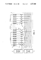
- the marking array 29 comprises a large area substrate 42 (represented by the dotted outline in FIG. 2) along one edge of which are formed an array of modulation electrodes (E) 28, a multiplexed data entry or loading circuit, comprising a small number of address bus lines (A) 44 and data bus lines (D) 46, and thin film switching elements 33, on for each electrode. With this array it is possible to directly address each electrode with only the small number of wire bonds needed to interface the electrodes with the external driver circuits 54 and 46.
- the switches 38 are preferably amorphous silicon transistors (a-Si:H TFTs), although other materials such as polycrystalline Si, laser annealed Si, CdS, Te, or ZnO may be used.
- a-Si:H TFTs amorphous silicon transistors
- each modulation electrode 28 is connected to the drain electrode 48 of the thin film transistor by a conductive trace
- an address bus line 44 is connected to the gate electrode 50
- a data bus line 46 is connected to the source electrode 52.
- the low temperature a-Si:H fabrication process allows a large degree of freedom in the choice of substrate materials, enabling the use of inexpensive amorphous materials such as glass, ceramics and possibly some printed circuit board materials.
- the substrate is glass and the modulating electrodes, the address and data buses are aluminum.
- Aluminum is the material of choice because it is compatible with the a-Si:H processing and makes good contacts with the source, drain and gate electrodes of the a-Si:H TFTs.
- the aluminum modulation electrodes have been found to oxidize rapidly when used in the ionographic process because they are subjected to the corrosive effluents from the corona chamber 12. Since the other aluminum elements are protected and are not contacted by the effluents they are unaffected. It is the purpose of this invention to retain the above-stated benefits of aluminum as the marking array material of choice while extending the lifetime of the modulation electrodes in the corrosive atmosphere.
- Our invention relates to applying a small bias potential, on the order of 1 to 2 volts across the ion modulation region 26 so as to drive the ions away from the modulation electrodes 28 and toward the opposite wall 40. This will prevent collision of the ions against the surface of the electrodes which action abets rapid oxidation, as explained above. It should be understood that the bias potential need be sufficiently small so as not to interfere with the switching action required for "writing" control, whether binary or grey scale. It may be as high as about 10% of the OFF voltage without significant adverse consequences.
- the curve of FIG. 3 plots modulation voltage against ion output current for an ideal cause (i.e. it is symmetric about 0 volts). It can be seen that the maximum ion output current is available when 0 volts is applied to the modulation electrodes, or stated another way, when there is no relative bias across the ion modulation region 26. Ion output current is pinched off at a relative bias of about 15 to 20 volts.
- the area of interest relative to the oxidation prevention bias is the upper portion of the curve where there is very little drop off in ion current for small changes in modulation voltage. Thus, a 10% (about 1.5 to 2.0 volts) bias will be seen to have very little effect on ion output current.
- the oxidation prevention potential may be applied in a number of different ways. It may be applied directly to each of the modulation electrodes by selecting the reference potential source 37 to be in the range of 0.75 to 2.5 volts above the bias applied to the opposite wall 40. Alternatively, the reference potential source 18, connected to the head 10 may be negatively biased relative to the bias applied to the modulation electrodes. Relative bias between the control elements across the ion modulation region also can be achieved by virtue of differences in materials electrically connected together.
- the head is made of a first material (e.g., stainless steel) and the modulation electrodes are made of a second material (e.g., aluminum) and these elements are connected to one another by means of a common ground
- a potential difference will exist between the two materials. This will be manifested by a bias across the ion modulation region which is straddled by these disparate materials.
- the potential difference is equal to the difference in work functions of the materials.
- the stainless steel head may have a work function on the order of 4 electron-volts and the aluminum electrodes may have a work function on the order of 3 electron-volts.
- an inherent bias of 1 volt is present across the ion modulation region 26 by virtue of the different materials being connected to a common ground.
- FIG. 4 there is shown a test device marking array 29' whose modulation electrodes 28 have been grouped in segments and shorted together so that it is possible to impose the same bias on all of the electrodes in each segment. Then the test device was run in an ionographic recording apparatus and after about 100 hours operation at room temperature and at room RH the corrosive effects were studied. It can be seen that different biases were imposed on the nine segments, with the exception that the bias imposed on the end segments 1 and 9 was repeated on segments 3 and 7, respectively, because the end segments had to be discounted due to non-uniform ion flow at these locations in the test apparatus.
Landscapes
- Engineering & Computer Science (AREA)
- Multimedia (AREA)
- Signal Processing (AREA)
- Physics & Mathematics (AREA)
- General Physics & Mathematics (AREA)
- Printers Or Recording Devices Using Electromagnetic And Radiation Means (AREA)
- Electrophotography Using Other Than Carlson'S Method (AREA)
Abstract
Description
Claims (9)
Priority Applications (1)
| Application Number | Priority Date | Filing Date | Title |
|---|---|---|---|
| US07/042,131 US4727388A (en) | 1987-04-24 | 1987-04-24 | Marking array having improved corrosion resistance |
Applications Claiming Priority (1)
| Application Number | Priority Date | Filing Date | Title |
|---|---|---|---|
| US07/042,131 US4727388A (en) | 1987-04-24 | 1987-04-24 | Marking array having improved corrosion resistance |
Publications (1)
| Publication Number | Publication Date |
|---|---|
| US4727388A true US4727388A (en) | 1988-02-23 |
Family
ID=21920205
Family Applications (1)
| Application Number | Title | Priority Date | Filing Date |
|---|---|---|---|
| US07/042,131 Expired - Lifetime US4727388A (en) | 1987-04-24 | 1987-04-24 | Marking array having improved corrosion resistance |
Country Status (1)
| Country | Link |
|---|---|
| US (1) | US4727388A (en) |
Cited By (10)
| Publication number | Priority date | Publication date | Assignee | Title |
|---|---|---|---|---|
| US4837591A (en) * | 1988-05-02 | 1989-06-06 | Xerox Corporation | Highlight color imaging by depositing positive and negative ions on a substrate |
| US4853719A (en) * | 1988-12-14 | 1989-08-01 | Xerox Corporation | Coated ion projection printing head |
| US4879194A (en) * | 1988-05-02 | 1989-11-07 | Xerox Corporation | Tri-level, highlight color imaging using ionography |
| US5062364A (en) * | 1989-03-29 | 1991-11-05 | Presstek, Inc. | Plasma-jet imaging method |
| US5138349A (en) * | 1990-09-20 | 1992-08-11 | Xerox Corporation | Apparatus for reducing the effects of ambient humidity variations upon an ionographic printing device |
| US5163368A (en) * | 1988-08-19 | 1992-11-17 | Presst, Inc. | Printing apparatus with image error correction and ink regulation control |
| US5235914A (en) * | 1988-08-19 | 1993-08-17 | Presstek, Inc. | Apparatus and method for imaging lithographic printing plates using spark discharges |
| US5237923A (en) * | 1988-08-19 | 1993-08-24 | Presstek, Inc. | Apparatus and method for imaging lithographic printing plates using spark discharges |
| US5270729A (en) * | 1991-06-21 | 1993-12-14 | Xerox Corporation | Ionographic beam positioning and crosstalk correction using grey levels |
| US5272979A (en) * | 1989-03-29 | 1993-12-28 | Presstek, Inc. | Plasma-jet imaging apparatus and method |
Citations (2)
| Publication number | Priority date | Publication date | Assignee | Title |
|---|---|---|---|---|
| US4584592A (en) * | 1984-08-13 | 1986-04-22 | Xerox Corporation | Marking head for fluid jet assisted ion projection imaging systems |
| US4646163A (en) * | 1985-10-07 | 1987-02-24 | Xerox Corporation | Ion projection copier |
-
1987
- 1987-04-24 US US07/042,131 patent/US4727388A/en not_active Expired - Lifetime
Patent Citations (2)
| Publication number | Priority date | Publication date | Assignee | Title |
|---|---|---|---|---|
| US4584592A (en) * | 1984-08-13 | 1986-04-22 | Xerox Corporation | Marking head for fluid jet assisted ion projection imaging systems |
| US4646163A (en) * | 1985-10-07 | 1987-02-24 | Xerox Corporation | Ion projection copier |
Cited By (11)
| Publication number | Priority date | Publication date | Assignee | Title |
|---|---|---|---|---|
| US4837591A (en) * | 1988-05-02 | 1989-06-06 | Xerox Corporation | Highlight color imaging by depositing positive and negative ions on a substrate |
| US4879194A (en) * | 1988-05-02 | 1989-11-07 | Xerox Corporation | Tri-level, highlight color imaging using ionography |
| EP0340996A3 (en) * | 1988-05-02 | 1990-09-05 | Xerox Corporation | Tri-level, highlight color imaging using ionography |
| US5163368A (en) * | 1988-08-19 | 1992-11-17 | Presst, Inc. | Printing apparatus with image error correction and ink regulation control |
| US5235914A (en) * | 1988-08-19 | 1993-08-17 | Presstek, Inc. | Apparatus and method for imaging lithographic printing plates using spark discharges |
| US5237923A (en) * | 1988-08-19 | 1993-08-24 | Presstek, Inc. | Apparatus and method for imaging lithographic printing plates using spark discharges |
| US4853719A (en) * | 1988-12-14 | 1989-08-01 | Xerox Corporation | Coated ion projection printing head |
| US5062364A (en) * | 1989-03-29 | 1991-11-05 | Presstek, Inc. | Plasma-jet imaging method |
| US5272979A (en) * | 1989-03-29 | 1993-12-28 | Presstek, Inc. | Plasma-jet imaging apparatus and method |
| US5138349A (en) * | 1990-09-20 | 1992-08-11 | Xerox Corporation | Apparatus for reducing the effects of ambient humidity variations upon an ionographic printing device |
| US5270729A (en) * | 1991-06-21 | 1993-12-14 | Xerox Corporation | Ionographic beam positioning and crosstalk correction using grey levels |
Similar Documents
| Publication | Publication Date | Title |
|---|---|---|
| US4584592A (en) | Marking head for fluid jet assisted ion projection imaging systems | |
| US4727388A (en) | Marking array having improved corrosion resistance | |
| US5508723A (en) | Electric field potential control device for an image forming apparatus | |
| US4794412A (en) | Vertical line width control ionographic system | |
| US5576742A (en) | Image recording head having corrosion resistant control electrodes | |
| US4779107A (en) | Modulation electrodes having improved corrosion resistance | |
| US7789489B2 (en) | Print head and image forming apparatus including the same | |
| JP4141617B2 (en) | Charge generation device, charging device, and image forming apparatus | |
| US4646163A (en) | Ion projection copier | |
| US4743925A (en) | Modulation electrodes having improved corrosion resistance | |
| US4972212A (en) | Method and apparatus for controlling ion trajectory perturbations in ionographic devices | |
| US6650349B2 (en) | Image forming apparatus having writing electrodes as a writing device | |
| US4973994A (en) | Method and apparatus for controlling ion trajectory perturbations in ionographic devices | |
| US4899186A (en) | Ionographic device with pin array coronode | |
| US4875062A (en) | Ion projection print head | |
| US4719481A (en) | Electrographic ion writing head driver system | |
| EP0341050A2 (en) | Ionographic marking head | |
| JPH04292960A (en) | Image forming device | |
| US5717449A (en) | Toner projection printer with improved address electrode structure | |
| US5138349A (en) | Apparatus for reducing the effects of ambient humidity variations upon an ionographic printing device | |
| Sheridon | Practical air-assisted ionographic printing | |
| US5455660A (en) | Electrical method and apparatus to control corona effluents | |
| US5072243A (en) | Electrostatic purge for an ion projection device | |
| JP3033313B2 (en) | Ion flow control electrostatic recording head | |
| JPS61174569A (en) | ion generator |
Legal Events
| Date | Code | Title | Description |
|---|---|---|---|
| AS | Assignment |
Owner name: XEROX CORPORATION, STAMFORD, CT. A CORP. OF NEW YO Free format text: ASSIGNMENT OF ASSIGNORS INTEREST.;ASSIGNORS:SHERIDON, NICHOLAS K.;SANG, HENRY W. JR.;REEL/FRAME:004717/0516 Effective date: 19870424 |
|
| STCF | Information on status: patent grant |
Free format text: PATENTED CASE |
|
| FPAY | Fee payment |
Year of fee payment: 4 |
|
| FEPP | Fee payment procedure |
Free format text: PAYOR NUMBER ASSIGNED (ORIGINAL EVENT CODE: ASPN); ENTITY STATUS OF PATENT OWNER: LARGE ENTITY |
|
| FPAY | Fee payment |
Year of fee payment: 8 |
|
| FPAY | Fee payment |
Year of fee payment: 12 |
|
| AS | Assignment |
Owner name: BANK ONE, NA, AS ADMINISTRATIVE AGENT, ILLINOIS Free format text: SECURITY INTEREST;ASSIGNOR:XEROX CORPORATION;REEL/FRAME:013153/0001 Effective date: 20020621 |
|
| AS | Assignment |
Owner name: JPMORGAN CHASE BANK, AS COLLATERAL AGENT, TEXAS Free format text: SECURITY AGREEMENT;ASSIGNOR:XEROX CORPORATION;REEL/FRAME:015134/0476 Effective date: 20030625 Owner name: JPMORGAN CHASE BANK, AS COLLATERAL AGENT,TEXAS Free format text: SECURITY AGREEMENT;ASSIGNOR:XEROX CORPORATION;REEL/FRAME:015134/0476 Effective date: 20030625 |
|
| AS | Assignment |
Owner name: XEROX CORPORATION, CONNECTICUT Free format text: RELEASE BY SECURED PARTY;ASSIGNOR:JPMORGAN CHASE BANK, N.A. AS SUCCESSOR-IN-INTEREST ADMINISTRATIVE AGENT AND COLLATERAL AGENT TO JPMORGAN CHASE BANK;REEL/FRAME:066728/0193 Effective date: 20220822 |