US4710476A - Surface-derivatized semiconductors with chemically sensitive luminescence - Google Patents
Surface-derivatized semiconductors with chemically sensitive luminescence Download PDFInfo
- Publication number
- US4710476A US4710476A US06/811,511 US81151185A US4710476A US 4710476 A US4710476 A US 4710476A US 81151185 A US81151185 A US 81151185A US 4710476 A US4710476 A US 4710476A
- Authority
- US
- United States
- Prior art keywords
- radiation
- semiconductor
- emitting surface
- reacted material
- radiation emitting
- Prior art date
- Legal status (The legal status is an assumption and is not a legal conclusion. Google has not performed a legal analysis and makes no representation as to the accuracy of the status listed.)
- Expired - Fee Related
Links
- 239000004065 semiconductor Substances 0.000 title claims abstract description 43
- 238000004020 luminiscence type Methods 0.000 title description 4
- 230000005855 radiation Effects 0.000 claims abstract description 50
- 239000000126 substance Substances 0.000 claims abstract description 4
- 239000000463 material Substances 0.000 claims description 15
- 150000001875 compounds Chemical class 0.000 claims description 14
- 239000011669 selenium Substances 0.000 claims description 10
- 238000000034 method Methods 0.000 claims description 8
- 230000005684 electric field Effects 0.000 claims description 7
- BUGBHKTXTAQXES-UHFFFAOYSA-N Selenium Chemical compound [Se] BUGBHKTXTAQXES-UHFFFAOYSA-N 0.000 claims description 6
- 229910052793 cadmium Inorganic materials 0.000 claims description 6
- BDOSMKKIYDKNTQ-UHFFFAOYSA-N cadmium atom Chemical compound [Cd] BDOSMKKIYDKNTQ-UHFFFAOYSA-N 0.000 claims description 6
- 238000009826 distribution Methods 0.000 claims description 6
- 238000006479 redox reaction Methods 0.000 claims description 6
- 229910052711 selenium Inorganic materials 0.000 claims description 6
- NINIDFKCEFEMDL-UHFFFAOYSA-N Sulfur Chemical compound [S] NINIDFKCEFEMDL-UHFFFAOYSA-N 0.000 claims description 5
- 230000008569 process Effects 0.000 claims description 5
- 229910052717 sulfur Inorganic materials 0.000 claims description 5
- 239000011593 sulfur Substances 0.000 claims description 5
- 230000001590 oxidative effect Effects 0.000 claims description 4
- 239000007787 solid Substances 0.000 claims description 4
- -1 ferrocene compound Chemical class 0.000 claims description 3
- HCHKCACWOHOZIP-UHFFFAOYSA-N Zinc Chemical compound [Zn] HCHKCACWOHOZIP-UHFFFAOYSA-N 0.000 claims 4
- 239000011701 zinc Substances 0.000 claims 4
- 229910052725 zinc Inorganic materials 0.000 claims 4
- GYHNNYVSQQEPJS-UHFFFAOYSA-N Gallium Chemical compound [Ga] GYHNNYVSQQEPJS-UHFFFAOYSA-N 0.000 claims 3
- 229910052733 gallium Inorganic materials 0.000 claims 3
- OAICVXFJPJFONN-UHFFFAOYSA-N Phosphorus Chemical compound [P] OAICVXFJPJFONN-UHFFFAOYSA-N 0.000 claims 2
- 229910052785 arsenic Inorganic materials 0.000 claims 2
- RQNWIZPPADIBDY-UHFFFAOYSA-N arsenic atom Chemical compound [As] RQNWIZPPADIBDY-UHFFFAOYSA-N 0.000 claims 2
- 229910052698 phosphorus Inorganic materials 0.000 claims 2
- 239000011574 phosphorus Substances 0.000 claims 2
- 229910052782 aluminium Inorganic materials 0.000 claims 1
- XAGFODPZIPBFFR-UHFFFAOYSA-N aluminium Chemical compound [Al] XAGFODPZIPBFFR-UHFFFAOYSA-N 0.000 claims 1
- 230000001678 irradiating effect Effects 0.000 claims 1
- 230000004075 alteration Effects 0.000 abstract description 3
- 238000005424 photoluminescence Methods 0.000 description 7
- 229910001218 Gallium arsenide Inorganic materials 0.000 description 5
- 239000011248 coating agent Substances 0.000 description 4
- 238000000576 coating method Methods 0.000 description 4
- WEVYAHXRMPXWCK-UHFFFAOYSA-N Acetonitrile Chemical compound CC#N WEVYAHXRMPXWCK-UHFFFAOYSA-N 0.000 description 3
- 239000007800 oxidant agent Substances 0.000 description 3
- 230000003647 oxidation Effects 0.000 description 3
- 238000007254 oxidation reaction Methods 0.000 description 3
- 239000000758 substrate Substances 0.000 description 3
- XLYOFNOQVPJJNP-UHFFFAOYSA-N water Substances O XLYOFNOQVPJJNP-UHFFFAOYSA-N 0.000 description 3
- OAKJQQAXSVQMHS-UHFFFAOYSA-N Hydrazine Chemical compound NN OAKJQQAXSVQMHS-UHFFFAOYSA-N 0.000 description 2
- 230000008859 change Effects 0.000 description 2
- 239000003638 chemical reducing agent Substances 0.000 description 2
- 238000001212 derivatisation Methods 0.000 description 2
- 238000006073 displacement reaction Methods 0.000 description 2
- 230000000694 effects Effects 0.000 description 2
- 238000005401 electroluminescence Methods 0.000 description 2
- 238000005530 etching Methods 0.000 description 2
- KTWOOEGAPBSYNW-UHFFFAOYSA-N ferrocene Chemical compound [Fe+2].C=1C=C[CH-]C=1.C=1C=C[CH-]C=1 KTWOOEGAPBSYNW-UHFFFAOYSA-N 0.000 description 2
- 229910052751 metal Inorganic materials 0.000 description 2
- 239000002184 metal Substances 0.000 description 2
- 239000000047 product Substances 0.000 description 2
- 230000009467 reduction Effects 0.000 description 2
- ZAMOUSCENKQFHK-UHFFFAOYSA-N Chlorine atom Chemical compound [Cl] ZAMOUSCENKQFHK-UHFFFAOYSA-N 0.000 description 1
- 229910003556 H2 SO4 Inorganic materials 0.000 description 1
- UFHFLCQGNIYNRP-UHFFFAOYSA-N Hydrogen Chemical compound [H][H] UFHFLCQGNIYNRP-UHFFFAOYSA-N 0.000 description 1
- NHTMVDHEPJAVLT-UHFFFAOYSA-N Isooctane Chemical compound CC(C)CC(C)(C)C NHTMVDHEPJAVLT-UHFFFAOYSA-N 0.000 description 1
- 238000010521 absorption reaction Methods 0.000 description 1
- 230000004888 barrier function Effects 0.000 description 1
- UHYPYGJEEGLRJD-UHFFFAOYSA-N cadmium(2+);selenium(2-) Chemical compound [Se-2].[Cd+2] UHYPYGJEEGLRJD-UHFFFAOYSA-N 0.000 description 1
- 239000007795 chemical reaction product Substances 0.000 description 1
- 239000000460 chlorine Substances 0.000 description 1
- 229910052801 chlorine Inorganic materials 0.000 description 1
- 238000002484 cyclic voltammetry Methods 0.000 description 1
- 230000006378 damage Effects 0.000 description 1
- 230000001419 dependent effect Effects 0.000 description 1
- MROCJMGDEKINLD-UHFFFAOYSA-N dichlorosilane Chemical compound Cl[SiH2]Cl MROCJMGDEKINLD-UHFFFAOYSA-N 0.000 description 1
- JVSWJIKNEAIKJW-UHFFFAOYSA-N dimethyl-hexane Natural products CCCCCC(C)C JVSWJIKNEAIKJW-UHFFFAOYSA-N 0.000 description 1
- 239000002019 doping agent Substances 0.000 description 1
- 239000003792 electrolyte Substances 0.000 description 1
- 239000000835 fiber Substances 0.000 description 1
- 239000007789 gas Substances 0.000 description 1
- 229910052739 hydrogen Inorganic materials 0.000 description 1
- 239000001257 hydrogen Substances 0.000 description 1
- 230000002427 irreversible effect Effects 0.000 description 1
- 238000004519 manufacturing process Methods 0.000 description 1
- 230000003287 optical effect Effects 0.000 description 1
- 238000002360 preparation method Methods 0.000 description 1
- 238000010791 quenching Methods 0.000 description 1
- SBIBMFFZSBJNJF-UHFFFAOYSA-N selenium;zinc Chemical compound [Se]=[Zn] SBIBMFFZSBJNJF-UHFFFAOYSA-N 0.000 description 1
- 230000035945 sensitivity Effects 0.000 description 1
- 238000000926 separation method Methods 0.000 description 1
- 230000003595 spectral effect Effects 0.000 description 1
- 239000003115 supporting electrolyte Substances 0.000 description 1
Images
Classifications
-
- G—PHYSICS
- G01—MEASURING; TESTING
- G01N—INVESTIGATING OR ANALYSING MATERIALS BY DETERMINING THEIR CHEMICAL OR PHYSICAL PROPERTIES
- G01N21/00—Investigating or analysing materials by the use of optical means, i.e. using sub-millimetre waves, infrared, visible or ultraviolet light
- G01N21/62—Systems in which the material investigated is excited whereby it emits light or causes a change in wavelength of the incident light
- G01N21/63—Systems in which the material investigated is excited whereby it emits light or causes a change in wavelength of the incident light optically excited
- G01N21/64—Fluorescence; Phosphorescence
- G01N21/6428—Measuring fluorescence of fluorescent products of reactions or of fluorochrome labelled reactive substances, e.g. measuring quenching effects, using measuring "optrodes"
- G01N21/643—Measuring fluorescence of fluorescent products of reactions or of fluorochrome labelled reactive substances, e.g. measuring quenching effects, using measuring "optrodes" non-biological material
-
- G—PHYSICS
- G01—MEASURING; TESTING
- G01N—INVESTIGATING OR ANALYSING MATERIALS BY DETERMINING THEIR CHEMICAL OR PHYSICAL PROPERTIES
- G01N21/00—Investigating or analysing materials by the use of optical means, i.e. using sub-millimetre waves, infrared, visible or ultraviolet light
- G01N21/62—Systems in which the material investigated is excited whereby it emits light or causes a change in wavelength of the incident light
- G01N21/63—Systems in which the material investigated is excited whereby it emits light or causes a change in wavelength of the incident light optically excited
- G01N21/64—Fluorescence; Phosphorescence
- G01N21/6428—Measuring fluorescence of fluorescent products of reactions or of fluorochrome labelled reactive substances, e.g. measuring quenching effects, using measuring "optrodes"
- G01N2021/6439—Measuring fluorescence of fluorescent products of reactions or of fluorochrome labelled reactive substances, e.g. measuring quenching effects, using measuring "optrodes" with indicators, stains, dyes, tags, labels, marks
Definitions
- the present invention relates to optically coupled chemical sensing devices and to processes for detecting the presence of certain classes of chemical compounds.
- Electroluminescence occurs in semiconductor materials which are capable of emitting visible or near visible radiation when an electrical current passes through the semiconductor. Photoluminescence can also occur in these materials. If external light is used to excite the semiconductor, a characteristic wavelength of light is emitted. These characteristic wavelengths vary amongst different photoluminescent semiconductors and can be varied in a single semiconductor by doping or changing the composition of the material.
- Luminescent Photoelectrochemical Cells Streckert, H. H., Tong, J. and Ellis, A. B., J. Am. Chem. Soc., Vol. 104, No. 2, 1982, pp. 581-588. It is noted therein that the intensity of light emitted by electroluminescence and photoluminescence varies directly with the applied voltage. The efficiency of charge transfer and good electrical contact at the surface is also noted as important in the efficiency of the process.
- U.S. Pat. No. 4,211,586 discloses a method of forming a multicolor light-emitting array of diodes.
- the diodes are formed by differentially etching a graded n-type semiconductor and diffusing a p-type dopant into the surface of the n-type semiconductor to form a p-n junction diode.
- U.S. patent application Ser. No. 712,799, filed Mar. 18, 1985 discloses an apparatus for detecting the presence of certain chemical compounds comprising a photoluminescent semiconductor having a metal coating on a radiation emitting surface of the semiconductor, a source of actinic radiation which can impinge on the radiation emitting surface of the semiconductor, and a means for detecting changes in the characteristics of radiation emitted from said radiation emitting surface.
- the absorption of hydrogen into the metal layer is suggested as varying the height of the Schottky barrier of the diode and causing a change in spectral characteristics of the radiation emitted.
- the present invention describes an optically coupled sensing apparatus of a photoluminescent semiconductor, a source of actinic radiation which can impinge on a radiation emitting surface of the semiconductor and a means for detecting changes in the characteristics of the radiation emitted from the radiation emitting surface.
- the radiation emitting surface has reacted thereon a compound capable of undergoing oxidation and/or reduction, the redox product of which reacted compound has a vertical charge distribution therein with respect to the radiation emitting surface.
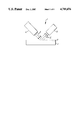
- the FIGURE shows a schematic representation of the sensing apparatus of the present invention.
- the FIGURE shows a schematic representation of the sensing device (1) of the present invention.
- the photoluminescent semiconductor layer (2) has a layer (4) of a compound capable of undergoing further oxidation or reduction reacted onto the surface of the semiconductor layer (2).
- a source (6) of actinic radiation (8) is provided to direct radiation (8) at the semiconductor layer (2).
- a detector (10) is provided to detect changes in the radiation (12) emitted from the semiconductor layer (2).
- the present invention uses the creation of electrical or ionic charges in compounds on the surface of photoluminescent semiconductors to alter or modulate the electric field of the semiconductor.
- the modulation of the electric field alters the photoluminescence of the semiconductor, and this alteration can be detected by sensing means.
- a compound can be coated or preferably reacted onto the surface of the semiconductor.
- the coated material or reacted compound must be capable of a further redox reaction.
- the product of the redox reaction must be a moiety or moieties with a charge thereon or a separation of charges with a vertical displacement relative to the emitting surface of the photoluminescent semiconductor.
- the created charge distribution must have some vertical displacement therein or there will be no variation in the electric field. For example, if the redox reaction produced a change in positive or negative ionic centers on the redox reaction product which were equidistant from the semiconductor surface, there would be no alteration in the electric field.
- Photoluminescent semiconductors are well known in the art. They are generally solid state solutions of at least two or three elements which, when stimulated by actinic radiation, emit radiation. Both the actinic and emitted radiation are generally visible or near visible radiation (300-900 nm). When a coating over the radiation emitting surface of the semiconductor is a material (such as ferrocene derivatives) which when oxidized or reduced alters the electric field in the semiconductor surface, the luminescence of the semiconductor has been found to be altered. Variations in photoluminescence are an indication of the presence of such oxidizing and reducing compounds.
- n-type semiconductors which can be used to form the detectors according to the present invention are n-GaAs, n-GaAs x P 1-x (where x is from 0 to 1), CdS, CdSe, and CdS x Se 1-x (0 ⁇ x ⁇ 1) wherein the semiconductor may have a graded composition or not.
- Other useful semiconductors would be ZnSe:Al, Cd x Zn 1-x S(0 ⁇ x ⁇ 1), ZnS x Se 1-x (0 ⁇ x ⁇ 1), Cd x Zn 1-x Se(0 ⁇ x ⁇ 1), and the like.
- the redox reactive compound can be deposited on the elements according to standard manufacturing techniques and techniques shown by Wrighton, J. Am. Chem. Soc., 1979, 101, p. 6179.
- a functional apparatus for actually using this phenomenon for detecting the presence of volatile oxidants and reductants would have at least the following 3 components: the coated semiconductor, a source of actinic radiation directed at the radiation emitting surface of the structure or sensor formed by the coating on the semiconductor, and an optical detector.
- the sensor or structure has already been described.
- the actinic radiation source may be merely an opening exposing the sensor or structure to available light (room light, sunlight, etc.) or may be any internal source of radiation such as a light bulb, light emitting diode, or laser.
- the radiometer may be selected from amongst the many commercially available radiometers, its selection being primarily dependent upon the ultimate sensitivity desired in the final article.
- Fiber optics may be used to carry actinic radiation to the diode or to carry emitted radiation away from the diode.
- n-GaAs were prepared for derivatization by etching in 4:1:1 H 2 SO 4 :H 2 O 2 (30% aqueous):H 2 O at 50° C. for 30 seconds, rinsed in water, immersed in 7M KOH at 50° C. for 30 minutes, rinsed again, and air-dried prior to derivatization.
- the samples prior to preparation were noted as n-GaAs:Te with carrier concentrations of 8 ⁇ 10 16 cm -3 and ⁇ 100> orientation.
- a ferrocene derivative, (1,1'-ferrocenediyl)dichlorosilane was reacted with the n-GaAs substrate in isooctane solution according to the teachings of Wrighton, J. Am. Chem. Soc., 1979, 101, p. 6179.
- the bandgap photoluminescence (PL) of the GaAs substrate (865 nm in the near IR) was sensitive to gaseous oxidants.
- gaseous I 2 or Br 2 caused the PL intensity to quench approximately 50%.
- This effect appeared to be irreversible in air, although strong volatile reducing agents such as hydrazine reversed the effect.
- the system was also regenerated by using the sample as an electrode in acetonitrile (n-Et 4 N + BF 4 - supporting electrolyte) and applying a cathodic pulse to reduce the Fe to its original oxidation state.
- Cyclic voltammetry in this electrolyte indicated that the surface coating was present in at most several monolayers of coverage.
- the sensor was unaffected by gases such as air, CO, CH 4 , and H 2 in both the oxidized and reduced states.
- gases such as air, CO, CH 4 , and H 2 in both the oxidized and reduced states.
- high concentrations of water vapor in combination with strong oxidizing agents such as Br 2 or chlorine brought about the destruction of the sensor's surface.
- Example 1 was repeated except that the photoluminescent semiconductors used in the substrate were CdS, GaAs 0 .7 P 0 .3 and CdS 0 .9 Se 0 .1.
- the apparatus was found to detect the presence of Br 2 and NO 2 .
Landscapes
- Health & Medical Sciences (AREA)
- Immunology (AREA)
- Life Sciences & Earth Sciences (AREA)
- Physics & Mathematics (AREA)
- Chemical & Material Sciences (AREA)
- Nuclear Medicine, Radiotherapy & Molecular Imaging (AREA)
- Chemical Kinetics & Catalysis (AREA)
- Optics & Photonics (AREA)
- Molecular Biology (AREA)
- Analytical Chemistry (AREA)
- Biochemistry (AREA)
- General Health & Medical Sciences (AREA)
- General Physics & Mathematics (AREA)
- Pathology (AREA)
- Investigating Or Analysing Materials By The Use Of Chemical Reactions (AREA)
- Investigating, Analyzing Materials By Fluorescence Or Luminescence (AREA)
- Led Devices (AREA)
Abstract
The presence of certain chemicals on the emitting surface of the surface-derivatized photoluminescent semiconductor alters the characteristics of radiation emitted from said surface. This alteration is used to indicate the presence of those chemicals in the environment.
Description
The present invention relates to optically coupled chemical sensing devices and to processes for detecting the presence of certain classes of chemical compounds.
Electroluminescence occurs in semiconductor materials which are capable of emitting visible or near visible radiation when an electrical current passes through the semiconductor. Photoluminescence can also occur in these materials. If external light is used to excite the semiconductor, a characteristic wavelength of light is emitted. These characteristic wavelengths vary amongst different photoluminescent semiconductors and can be varied in a single semiconductor by doping or changing the composition of the material.
Amongst the various studies on the luminescence of photostimulated or electroluminescent materials is "Luminescent Photoelectrochemical Cells", Streckert, H. H., Tong, J. and Ellis, A. B., J. Am. Chem. Soc., Vol. 104, No. 2, 1982, pp. 581-588. It is noted therein that the intensity of light emitted by electroluminescence and photoluminescence varies directly with the applied voltage. The efficiency of charge transfer and good electrical contact at the surface is also noted as important in the efficiency of the process.
U.S. patent application Ser. No. 480,471 filed on Mar. 30, 1983 discloses semiconductor electrodes having multicolor luminescence. These semiconductors comprise solid state solutions of three elements which vary in a vertically anisotropic manner. The preferred solid state solutions are of cadmium, sulfur and selenium.
U.S. Pat. No. 4,211,586 discloses a method of forming a multicolor light-emitting array of diodes. The diodes are formed by differentially etching a graded n-type semiconductor and diffusing a p-type dopant into the surface of the n-type semiconductor to form a p-n junction diode.
U.S. patent application Ser. No. 712,799, filed Mar. 18, 1985, discloses an apparatus for detecting the presence of certain chemical compounds comprising a photoluminescent semiconductor having a metal coating on a radiation emitting surface of the semiconductor, a source of actinic radiation which can impinge on the radiation emitting surface of the semiconductor, and a means for detecting changes in the characteristics of radiation emitted from said radiation emitting surface. The absorption of hydrogen into the metal layer is suggested as varying the height of the Schottky barrier of the diode and causing a change in spectral characteristics of the radiation emitted.
The present invention describes an optically coupled sensing apparatus of a photoluminescent semiconductor, a source of actinic radiation which can impinge on a radiation emitting surface of the semiconductor and a means for detecting changes in the characteristics of the radiation emitted from the radiation emitting surface. The radiation emitting surface has reacted thereon a compound capable of undergoing oxidation and/or reduction, the redox product of which reacted compound has a vertical charge distribution therein with respect to the radiation emitting surface.
The FIGURE shows a schematic representation of the sensing apparatus of the present invention.
The FIGURE shows a schematic representation of the sensing device (1) of the present invention. The photoluminescent semiconductor layer (2) has a layer (4) of a compound capable of undergoing further oxidation or reduction reacted onto the surface of the semiconductor layer (2). A source (6) of actinic radiation (8) is provided to direct radiation (8) at the semiconductor layer (2). A detector (10) is provided to detect changes in the radiation (12) emitted from the semiconductor layer (2).
The present invention uses the creation of electrical or ionic charges in compounds on the surface of photoluminescent semiconductors to alter or modulate the electric field of the semiconductor. The modulation of the electric field alters the photoluminescence of the semiconductor, and this alteration can be detected by sensing means.
A compound can be coated or preferably reacted onto the surface of the semiconductor. The coated material or reacted compound must be capable of a further redox reaction. Furthermore, the product of the redox reaction must be a moiety or moieties with a charge thereon or a separation of charges with a vertical displacement relative to the emitting surface of the photoluminescent semiconductor. The created charge distribution must have some vertical displacement therein or there will be no variation in the electric field. For example, if the redox reaction produced a change in positive or negative ionic centers on the redox reaction product which were equidistant from the semiconductor surface, there would be no alteration in the electric field.
Photoluminescent semiconductors are well known in the art. They are generally solid state solutions of at least two or three elements which, when stimulated by actinic radiation, emit radiation. Both the actinic and emitted radiation are generally visible or near visible radiation (300-900 nm). When a coating over the radiation emitting surface of the semiconductor is a material (such as ferrocene derivatives) which when oxidized or reduced alters the electric field in the semiconductor surface, the luminescence of the semiconductor has been found to be altered. Variations in photoluminescence are an indication of the presence of such oxidizing and reducing compounds.
Particularly useful n-type semiconductors which can be used to form the detectors according to the present invention are n-GaAs, n-GaAsx P1-x (where x is from 0 to 1), CdS, CdSe, and CdSx Se1-x (0≦x≦1) wherein the semiconductor may have a graded composition or not. Other useful semiconductors would be ZnSe:Al, Cdx Zn1-x S(0≦x≦1), ZnSx Se1-x (0≦x≦1), Cdx Zn1-x Se(0≦x≦1), and the like. The redox reactive compound can be deposited on the elements according to standard manufacturing techniques and techniques shown by Wrighton, J. Am. Chem. Soc., 1979, 101, p. 6179.
A functional apparatus for actually using this phenomenon for detecting the presence of volatile oxidants and reductants would have at least the following 3 components: the coated semiconductor, a source of actinic radiation directed at the radiation emitting surface of the structure or sensor formed by the coating on the semiconductor, and an optical detector. The sensor or structure has already been described. The actinic radiation source may be merely an opening exposing the sensor or structure to available light (room light, sunlight, etc.) or may be any internal source of radiation such as a light bulb, light emitting diode, or laser. The radiometer may be selected from amongst the many commercially available radiometers, its selection being primarily dependent upon the ultimate sensitivity desired in the final article. Fiber optics may be used to carry actinic radiation to the diode or to carry emitted radiation away from the diode.
Samples of n-GaAs were prepared for derivatization by etching in 4:1:1 H2 SO4 :H2 O2 (30% aqueous):H2 O at 50° C. for 30 seconds, rinsed in water, immersed in 7M KOH at 50° C. for 30 minutes, rinsed again, and air-dried prior to derivatization. The samples prior to preparation were noted as n-GaAs:Te with carrier concentrations of 8×1016 cm-3 and <100> orientation. A ferrocene derivative, (1,1'-ferrocenediyl)dichlorosilane was reacted with the n-GaAs substrate in isooctane solution according to the teachings of Wrighton, J. Am. Chem. Soc., 1979, 101, p. 6179.
When the sensor was illuminated with ultrabandgap light, the bandgap photoluminescence (PL) of the GaAs substrate (865 nm in the near IR) was sensitive to gaseous oxidants. For example, gaseous I2 or Br2 caused the PL intensity to quench approximately 50%. This effect appeared to be irreversible in air, although strong volatile reducing agents such as hydrazine reversed the effect. The system was also regenerated by using the sample as an electrode in acetonitrile (n-Et4 N+ BF4 - supporting electrolyte) and applying a cathodic pulse to reduce the Fe to its original oxidation state. Cyclic voltammetry in this electrolyte indicated that the surface coating was present in at most several monolayers of coverage. The sensor was unaffected by gases such as air, CO, CH4, and H2 in both the oxidized and reduced states. Although somewhat resistant to water vapor, high concentrations of water vapor in combination with strong oxidizing agents such as Br2 or chlorine brought about the destruction of the sensor's surface.
Example 1 was repeated except that the photoluminescent semiconductors used in the substrate were CdS, GaAs0.7 P0.3 and CdS0.9 Se0.1. The apparatus was found to detect the presence of Br2 and NO2.
Claims (12)
1. An apparatus for detecting the presence of chemical compounds comprising:
(1) a photoluminescent semiconductor having on a radiation emitting surface thereof a reacted material bonded to said radiation emitting surface of said semiconductor, said reacted material being capable of undergoing a redox reaction with an oxidizing or reducing compound to produce a redox product bonded to said radiation emitting surface, which reacted material has an ionic charge distribution which is vertical with respect to the radiation emitting surface, said charge distribution being capable of altering an electric field in said semiconductor,
(2) a source of actinic radiation which impinges on said radiation emitting surface of said semiconductor, and
(3) a means for detecting changes in the radiation emitted from said radiation emitting surface.
2. The apparatus of claim 1 wherein said source of radiation comprises visible light.
3. The apparatus of claim 1 wherein said semiconductor comprises a solid state solution of at least two elements selected from the group consisting of (a) cadmium, selenium and sulfur, (b) zinc, selenium and sulfur, (c) cadmium, zinc and selenium, (d) cadmium, zinc and sulfur, (e) cadmium and selenium, (f) cadmium and sulfur, (g) zinc and selenium doped with aluminum, (h) gallium and arsenic, (i) gallium, arsenic and phosphorus, and (j) gallium and phosphorus.
4. The apparatus of claim 3 wherein said means for detecting changes in the characteristics of the radiation is a radiometer.
5. The apparatus of claim 3 wherein said reacted material comprises a ferrocene compound.
6. The apparatus of claim 1 wherein said means for detecting changes in the characteristics of the radiation is a radiometer.
7. The apparatus of claim 6 wherein said source of radiation comprises visible light.
8. The apparatus of claim 6 wherein said reacted material comprises a ferrocene compound.
9. The apparatus of claim 8 wherein said source of radiation comprises visible light.
10. The process for detecting the presence of chemical components comprising providing a photoluminescent semiconductor having on at least one radiation emitting surface a reacted material bonded to said radiation emitting surface, said reacted material being capable of undergoing a redox reaction with an oxidizing or reducing compound to produce a redox product bonded to said radiation emitting surface, which reacted material has an ionic charge distribution which is vertical with respect to the radiation emitting surface, said charge distribution being capable of altering an electric field in said semiconductor, irradiating said surface with actinic radiation, observing the radiation emitted from said surface, then exposing said surface to an environment having chemical compounds capable of oxidizing or reducing said reacted material therein and detecting any changes in the radiation emitted from said surface.
11. The process of claim 10 wherein said actinic radiation is visible light.
12. The process of claim 10 wherein light from a light bulb, laser, or light emitting diode provides said actinic radiation.
Priority Applications (4)
| Application Number | Priority Date | Filing Date | Title |
|---|---|---|---|
| US06/811,511 US4710476A (en) | 1985-12-20 | 1985-12-20 | Surface-derivatized semiconductors with chemically sensitive luminescence |
| JP61264867A JPS62147346A (en) | 1985-12-20 | 1986-11-06 | Semiconductor, which has chemical sensitive luminescence andsurface thereof is changed into derivative |
| DE86309759T DE3689002T2 (en) | 1985-12-20 | 1986-12-15 | Semiconductors modified on the surface with chemically sensitive luminescence. |
| EP86309759A EP0228855B1 (en) | 1985-12-20 | 1986-12-15 | Surface-derivatized semiconductors with chemically sensitive luminescence |
Applications Claiming Priority (1)
| Application Number | Priority Date | Filing Date | Title |
|---|---|---|---|
| US06/811,511 US4710476A (en) | 1985-12-20 | 1985-12-20 | Surface-derivatized semiconductors with chemically sensitive luminescence |
Publications (1)
| Publication Number | Publication Date |
|---|---|
| US4710476A true US4710476A (en) | 1987-12-01 |
Family
ID=25206760
Family Applications (1)
| Application Number | Title | Priority Date | Filing Date |
|---|---|---|---|
| US06/811,511 Expired - Fee Related US4710476A (en) | 1985-12-20 | 1985-12-20 | Surface-derivatized semiconductors with chemically sensitive luminescence |
Country Status (4)
| Country | Link |
|---|---|
| US (1) | US4710476A (en) |
| EP (1) | EP0228855B1 (en) |
| JP (1) | JPS62147346A (en) |
| DE (1) | DE3689002T2 (en) |
Cited By (7)
| Publication number | Priority date | Publication date | Assignee | Title |
|---|---|---|---|---|
| US5030419A (en) * | 1990-06-14 | 1991-07-09 | Ellis Arthur B | Wastewater pollutant sensor |
| EP0545523A3 (en) * | 1991-09-26 | 1994-02-09 | Shinetsu Handotai Kk | |
| US5319975A (en) * | 1992-07-16 | 1994-06-14 | Rutgers, The State University Of New Jersey | Fiber optic moisture sensor |
| US5766952A (en) * | 1996-07-25 | 1998-06-16 | Regents Of The University Of Minnesota | Vapochromic platinum-complexes and salts |
| US6368867B1 (en) | 1998-01-29 | 2002-04-09 | International Business Machines Corporation | Monitor for verification of ozone reaction |
| WO2003058692A1 (en) * | 2001-12-28 | 2003-07-17 | University And Community College System Of Nevada On Behalf Of The University Of Nevada, Reno | Redox-switchable materials |
| US20080110241A1 (en) * | 2004-05-17 | 2008-05-15 | Avner Rothschild | Photo-induced sensitivity and selectivity of semiconductor gas sensors |
Families Citing this family (1)
| Publication number | Priority date | Publication date | Assignee | Title |
|---|---|---|---|---|
| US4752588A (en) * | 1987-03-30 | 1988-06-21 | Minnesota Mining And Manufacturing Company | Luminescent chemical sensor for gases |
-
1985
- 1985-12-20 US US06/811,511 patent/US4710476A/en not_active Expired - Fee Related
-
1986
- 1986-11-06 JP JP61264867A patent/JPS62147346A/en active Pending
- 1986-12-15 DE DE86309759T patent/DE3689002T2/en not_active Expired - Fee Related
- 1986-12-15 EP EP86309759A patent/EP0228855B1/en not_active Expired - Lifetime
Non-Patent Citations (12)
| Title |
|---|
| "Chemically Derivatized n-Type Semiconducting Gallium Arsenide Photoelectrodes etc.", J. M. Bolts et al., J.A.C.S., 100, 1979, pp. 6179-6183. |
| "Covalently Attached Organic Monolayers on Semiconductor Surfaces", Ivan Haller, J.A.C.S., 100, 1978, pp. 8050-8055. |
| "Preparation of Chemically Derivatized Platinum etc", M. S. Wrighton et al., J.A.C.S., 100:23, Nov. 8, 1978, pp. 7264-7270. |
| "The Reduction of Iodine at GaAs: etc.", J.E.A.M. van der Meerakker, J. Electrochem. Soc. 30, 1985, pp. 435-440. |
| Carpender et al; Photoluminescent Response of Pd CdS and Pd CdS x Se 1-x Schottky Diodes to Molecular Hydrogen; Langmuir 1985 1, 605 607. * |
| Carpender et al; Photoluminescent Response of Pd-CdS and Pd-CdSx Se1-x Schottky Diodes to Molecular Hydrogen; Langmuir 1985 1, 605-607. |
| Chemically Derivatized n Type Semiconducting Gallium Arsenide Photoelectrodes etc. , J. M. Bolts et al., J.A.C.S., 100, 1979, pp. 6179 6183. * |
| Covalently Attached Organic Monolayers on Semiconductor Surfaces , Ivan Haller, J.A.C.S., 100, 1978, pp. 8050 8055. * |
| McQuarrie et al; General Chemistry; W. H. Freeman and Co., New York, 1984, pp. 781 803. * |
| McQuarrie et al; General Chemistry; W. H. Freeman and Co., New York, 1984, pp. 781-803. |
| Preparation of Chemically Derivatized Platinum etc , M. S. Wrighton et al., J.A.C.S., 100:23, Nov. 8, 1978, pp. 7264 7270. * |
| The Reduction of Iodine at GaAs: etc. , J.E.A.M. van der Meerakker, J. Electrochem. Soc. 30, 1985, pp. 435 440. * |
Cited By (9)
| Publication number | Priority date | Publication date | Assignee | Title |
|---|---|---|---|---|
| US5030419A (en) * | 1990-06-14 | 1991-07-09 | Ellis Arthur B | Wastewater pollutant sensor |
| WO1991019932A1 (en) * | 1990-06-14 | 1991-12-26 | Ellis Arthur B | Wastewater pollutant sensor |
| EP0545523A3 (en) * | 1991-09-26 | 1994-02-09 | Shinetsu Handotai Kk | |
| US5319975A (en) * | 1992-07-16 | 1994-06-14 | Rutgers, The State University Of New Jersey | Fiber optic moisture sensor |
| US5766952A (en) * | 1996-07-25 | 1998-06-16 | Regents Of The University Of Minnesota | Vapochromic platinum-complexes and salts |
| US6368867B1 (en) | 1998-01-29 | 2002-04-09 | International Business Machines Corporation | Monitor for verification of ozone reaction |
| WO2003058692A1 (en) * | 2001-12-28 | 2003-07-17 | University And Community College System Of Nevada On Behalf Of The University Of Nevada, Reno | Redox-switchable materials |
| US7435362B2 (en) | 2001-12-28 | 2008-10-14 | The Board Of Regents Of The Nevada System Of Higher Education On Behalf Of The University Of Navada | Redox-switchable materials |
| US20080110241A1 (en) * | 2004-05-17 | 2008-05-15 | Avner Rothschild | Photo-induced sensitivity and selectivity of semiconductor gas sensors |
Also Published As
| Publication number | Publication date |
|---|---|
| EP0228855A3 (en) | 1989-07-12 |
| EP0228855B1 (en) | 1993-09-08 |
| EP0228855A2 (en) | 1987-07-15 |
| DE3689002T2 (en) | 1994-03-31 |
| DE3689002D1 (en) | 1993-10-14 |
| JPS62147346A (en) | 1987-07-01 |
Similar Documents
| Publication | Publication Date | Title |
|---|---|---|
| US4081764A (en) | Zinc oxide light emitting diode | |
| Mettler | Photoluminescence as a tool for the study of the electronic surface properties of gallium arsenide | |
| US7227177B2 (en) | Doped semiconductor nanocrystals | |
| Richter et al. | Current-induced light emission from a porous silicon device | |
| Heimer et al. | Molecular level photovoltaics: the electrooptical properties of metal cyanide complexes anchored to titanium dioxide | |
| Peter | The photoelectrochemical properties of anodic cadmium sulphide films | |
| US4710476A (en) | Surface-derivatized semiconductors with chemically sensitive luminescence | |
| US4752588A (en) | Luminescent chemical sensor for gases | |
| Mitri et al. | Optical gas sensor based on the combination of a QD photoluminescent probe and a QD photodetector | |
| Balkanski et al. | Internal photoeffect and exciton diffusion in cadmium and zinc sulfides | |
| Allongue et al. | Charge transfer process at illuminated semiconductor/electrolyte junctions modified by electrodeposition of microscopic metal grain | |
| JPH011938A (en) | Luminescent chemical sensor for gas detection | |
| Gerischer | Photoassisted interfacial electron transfer | |
| US5030419A (en) | Wastewater pollutant sensor | |
| Iida | Luminescence in as-grown ZnSe crystals containing Cu impurity | |
| Ali et al. | Photodetector biased on ZnO nanoparticles/Poly-TPD organic material | |
| EP0195648B1 (en) | Diodes with chemically sensitive luminescence | |
| Thjeel et al. | Fabrication and characteristics of fast photo response ZnO/porous silicon UV photoconductive detector | |
| EP3811427B1 (en) | A photon multiplying film | |
| JPH0786461B2 (en) | How to measure humidity | |
| Arbour et al. | Surface chemistries and photoelectrochemistries of thin film molecular semiconductor materials | |
| Somani et al. | Sensitization effect in conducting polyaniline by rhodamine 6G | |
| Balberg et al. | Sensitization of the minority-carrier lifetime in a photoconductor | |
| Morehead et al. | The Dember Effect in ZnS‐Type Materials | |
| Musser et al. | Rhodamine B surface state hole traps |
Legal Events
| Date | Code | Title | Description |
|---|---|---|---|
| AS | Assignment |
Owner name: MINNESOTA MINING AND MANUFACTURING COMPANY, ST. PA Free format text: ASSIGNMENT OF ASSIGNORS INTEREST.;ASSIGNORS:ELLIS, ARTHUR B.;VAN RYSWYK, HAL;REEL/FRAME:004501/0019 Effective date: 19851219 |
|
| FPAY | Fee payment |
Year of fee payment: 4 |
|
| CC | Certificate of correction | ||
| REMI | Maintenance fee reminder mailed | ||
| LAPS | Lapse for failure to pay maintenance fees | ||
| FP | Lapsed due to failure to pay maintenance fee |
Effective date: 19951206 |
|
| STCH | Information on status: patent discontinuation |
Free format text: PATENT EXPIRED DUE TO NONPAYMENT OF MAINTENANCE FEES UNDER 37 CFR 1.362 |