The present invention relates to error correction in an apparatus for reproducing a digital signal and, more particularly, to an error correction method and a system which are suitable for decoding code words having a number of check words, such as in the decoding of Reed Solomon Codes.
In case of transmitting or recording a digital signal such as by a PCM recorder, the occurrence of error data in the transmission system becomes a problem. Therefore, check words are added when transmitting or recording and the error data is corrected using those check words upon reception or reproduction. As the check words, BCH codes and the like which have good efficiency and can be easily decoded are used. Particularly, Reed Solomon codes as one type of the BCH codes are usually used as the block codes. Further, cross-interleave codes are known as a method of increasing the correcting capability by performing double encoding by the use of these codes.
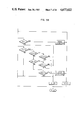
FIGS. 1 and 2 show well-known examples of an encoding circuit and a decoding circuit for the cross-interleave Reed Solomon codes (hereinbelow, abbreviated as CIRC codes), which circuits are respectively disclosed in GB No. 2076569A (Odaka et al, U.S. Pat. No. 4,413,340), and in BG No. 2079993A (Sako et al, U.S. Pat. No. 4,437,185). In FIG. 1, numerals 1 and 2 denote encoders; 3, 4 and 5 indicate interleave circuits; and 6 represents a data inverting circuit. In FIG. 2, numerals 7 and 8 denote decoders; and 9, 10 and 11 are deinterleave circuits.
In the CIRC codes, the double encoding by the use of Reed Solomon codes is performed. In the coding circuit of FIG. 1, after the first interleave was performed by the interleave circuit 3 with respect to 24 information words, check words Q1, Q2, Q3 and Q4 of four words are added by the encoder 1. Further, after the second interleave was performed by the interleave circuit 4 with regard to the code block of 28 words consisting of the 24 information words and four check words, check words P1, P2, P3, and P4 of four words are added by the encoder 2. The code block of 32 words consisting of 24 information words and eight check words is further subjected to the third interleave processing by the interleave circuit 5, and thereafter they are converted to serial data and this data is then transmitted or recorded. In addition, the check words are inverted by the data inverting circuit 6 for prevention of misdetection or miscorrection when sequential data is lost.
In the decoding circuit of FIG. 2, after the deinterleave corresponding to the above-mentioned third interleave was performed by the deinterleave circuit 9 and after the check words were again inverted by a data inverting circuit 6', the first decoding is done by the decoder 7. In this first decoding, the error detection and error correction by use of the check words P1 to P4 are executed. The 24 information words and four check words to which the error detection and error correction were done by the decoder 7 are deinterleaved .by the deinterleave circuit 10 corresponding to the foregoing second interleave, thereafter they are subjected to the second decoding by the decoder 8. In this second decoding, the error detection and error correction are performed by use of the check words Q1 to Q4. The 24 information words to which the error detection and error correction were done by the decoder 8 are deinterleaved by the deinterleave circuit 11 corresponding to the above-mentioned first interleave, then they are outputted.
In the method of performing the double encoding such as in the CIRC codes, the correcting capability can be raised by performing the decoding twice or more times by use of two different code blocks (P1 -P4 ; Q1 -Q4). The technology for raising the error correction capability is disclosed in GB No. 2079993A (U.S. Pat. No. 4,437,185 issued Mar. 13, 1984). However, in the conventional decoding method, only one or two words are corrected in the first decoding C1 and the second decoding C2, so that the correcting capability which the codes inherently have is not sufficiently made the most of. Also, the optimum decoding method in accordance with the state of flag upon the first decoding is not employed in the second decoding.
It is an object of the present invention to provide an error correction method and a system which can make the most of the error correcting capability which the codes inherently have in order to solve such problems.
The fundamental concept of the present invention is that in case of correcting the errors of p-words in the codes having a Hamming distance of d and in case of correcting the erasures of q-words in the same codes, plural decoding methods so as to satisfy the relation
2p+q=d-1
are used, thereby enabling the error correcting capability which the codes inherently have to be made the most of. The above decoding method is implemented by an error correcting system using programs.
In the accompanying drawings:
FIG. 1 is a diagram showing a prior art coding circuit for the CIRC codes;
FIG. 2 is a diagram showing a prior art decoding circuit for the CIRC codes;
FIG. 3 is a schematic flowchart showing the second decoding procedure for the CIRC codes according to the invention;
FIGS. 4, 4A, 4B and 5, 5A, 5B show detailed flowcharts of FIG. 3;
FIG. 6 is a block diagram showing a reproducing apparatus in which a system according to an embodiment of the present invention is incorporated;
FIGS. 7, 7A and 7B show a timing chart for error correction;
FIG. 8 is a block diagram of an error correction system according to an embodiment of the invention;
FIG. 9 is a diagram showing a syndrome generating circuit;
FIG. 10 is a diagram showing a multiplying/dividing circuit over GF (28);
FIG. 11 is a diagram showing an adder over GF (28);
FIG. 12 is a diagram showing the program arrangement;
FIGS. 13, 13A and 13B show one embodiment of the error correcting system of the invention;
FIG. 14 is a diagram showing an arithmetic logic circuit over Galois field;
FIG. 15 is a diagram showing the program arrangement;
FIGS. 16, 16A and 16B show another embodiment of the error correcting system of the invention;
FIG. 17 is a diagram showing an example of an arrangement of the multiplying circuit which is used in the invention;
FIG. 18 is a diagram showing the dividing circuit which is suitable for use in the invention;
FIG. 19 is a diagram showing the arithmetic logic circuit for performing the composite operations which is suitable for use in the invention; and
FIG. 20 shows a comparison diagram regarding the correcting capabilities by the present invention and the conventional example.
It will be described hereinbelow the case where one embodiment of the present invention is employed for the foregoing CIRC codes.
In the decoding of the CIRC codes, it is necessary to decode the Reed Solomon codes over Galois field GF (28) in which the code length is 32 words and the number of check words is four in the first decoding, and over GF (28) in which the code length is 28 words and the number of check words is four in the second decoding.
First, the Reed Solomon codes defined over Galois field GF (28) and a method of decoding the same will be described.
Assuming that one of the roots of the eighth-order irreducible polynomial F(x) over GF (28) is α, the set {0, 1, α, α2, . . . , α254 } of which the (28 -2) elements which are represented by the power of α were added to the elements of GF (2) constitutes GF (28). When a certain positive integer is t in GF (28), the Reed Solomon codes are the codes in which the code length n=(28 -1) and the number of information words is (n-2t) and the number of check words is 2t and which use the following generating polynomial,
g(x)=(x+1)(x+α)(x+α.sup.2) . . . (x+α.sup.2t-1),
or
g(x)=(x+α)(x+α.sup.2)(x+α.sup.3) . . . (x+α.sup.2t)(1)
Namely, in the Reed Solomon codes, the polynomial expression
C(x)=C.sub.0 +C.sub.1 x+C.sub.2 x.sup.2 +. . . +C.sub.n-1 x.sup.n-1 ( 2)
of the code word C={C0, C1, . . . , Cn-1 } can be divided by g(x). This is represented as the following expression.
C(x)≡0 (mod g(x)) (3)
The word length n can be reduced within a range of
2.sup.8 -1≧n>2t
A Hamming distance d is (2t+1) in these Reed Solomon codes.
When it is now assumed that the reception (reproduction) signal regarding the code word C(x) represented by expression (2) is
R(x)=r.sub.0 +r.sub.1 x+. . . +r.sub.n-1 x.sup.n-1 ( 4)
and that ν errors ##EQU1## occurred in this reception (reproduction) signal, ##EQU2## The errors E(x) can be obtained by syndromes Sk represented by the following expression. ##EQU3## As the decoding procedure, the error location polynomial ##EQU4## is first obtained from the syndrimes Sk and by obtaining its roots, the error locations ii, i2, . . . , i.sub.ν can be known. Since σ(αij)=0 from expression (8), ##EQU5## By adding the above expression with respect to 0≦k≦2t-1 (or 1≦k ≦2t),
S.sub.i σ.sub.ν +S.sub.i+1 σ.sub.ν-1 +. . . +S.sub.i+ν-1 σ.sub.1 +S.sub.i+ν =0(0≦i≦2t-1-ν or 1≦i≦2t-ν) (9)
is satisfied. The error locations σi can be obtained by solving expression (9). Further, by obtaining these error locations σi and error values ei.sbsb.1, ei.sbsb.2, . . . eiν from expression (7) to obtain E(x), the error correction can be performed by
C(x)=R(x)+E(x) (10)
In the codes having a Hamming distance of d, it is possible to correct the p errors and the q erasures within a range of
2p+q≦d-1
Since the Hamming distance is (2t+1) in the Reed Solomon codes, the error correction can be performed within a range of
2p+q≦2t
Next, a practical example of the decoding method will be shown with respect to the Reed Solomon codes in which t=2 and the number of information words is (n-4), the number of check words is four, and the generating polynomial is
g(x)=(x+1)(x+α)(x+α.sup.2)(x+α.sup.3) (11)
The syndromes S0, S1, S2 and S3 in this case are as follows. ##EQU6## When no error is detected, the following relation will be obviously satisfied.
S.sub.0 =S.sub.1 =S.sub.2 =S.sub.3 =0
In the case where the error of one word (error location is set to i) is detected, ##EQU7## from expression (9).
Therefore,
σ.sub.1 =S.sub.1 /S.sub.0 =S.sub.2 /S.sub.1 =S.sub.3 /S.sub.2
In addition, since ##EQU8## the error location i is obtained by
α.sup.i =S.sub.1 /S.sub.0 ( 14)
The error value in this case will be
e.sub.i =S.sub.0 ( 15)
from expression (7).
In the case where the errors of two words (error locations are set to i1 and i2) are detected, ##EQU9## from expression (9).
By solving the above expression, ##EQU10## will be obtained. Therefore, the error location polynomial will be ##EQU11## By solving σ(x)=0 with regard to expression (17), α i 1 and α i 2 are obtained, so that the error locations i1 and i2 can be derived. In addition, from expression (7), ##EQU12## Therefore, error values ei.sbsb.1 and ei.sbsb.2 can be derived from ##EQU13##
In the case where the errors of three words (error locations are set to i1, i2 and i3) are detected, from expression (9),
S.sub.0 σ.sub.3 +S.sub.1 σ.sub.2 +S.sub.2 σ.sub.1 +S.sub.3 =0 (20)
will be obtained.
Also,
σ(x)=(x+α.sup.i.sbsp.1)(x+α.sup.i .sbsp.2)(x+α.sup.i.sbsp.2) (21)
thus, ##EQU14## Consequently, if the error locations i1 and i2 are known, ##EQU15## will be obtained from expressions (20) and (22).
However, the third error location i3 can be obtained from
A.sub.1 =α.sup.i.sbsp.1.sup.+i.sbsp.2, A.sub.2 =α.sup.i.sbsp.1 +α.sup.i.sbsp.2
In addition, from expression (7), ##EQU16## Therefore ##EQU17##
However, the error values ei.sbsb.1, ei.sbsb.2 and ei.sbsb.3 can be obtained from
A.sub.3 =α.sup.i.sbsp.2 +α.sup.i.sbsp.3, A.sub.4 =α.sup.i.sbsp.3 +α.sup.i.sbsb.1
In the case where the errors of four words (error locations are set to i1, i2, i3 and i4) are detected, from expression (7), ##EQU18## Therefore, if the error locations i1 to i4 are known, ##EQU19## where
B.sub.1 =α.sup.i.sbsp.1 +α.sup.i.sbsp.4
B.sub.2 =B.sub.1 (α.sup.i.sbsp.2 +α.sup.i.sbsp.4)
B.sub.3 =B.sub.2 (α.sup.i.sbsp.3 +α.sup.i.sbsp.4)
C.sub.1 =S.sub.0 α.sup.i.sbsp.1 +S.sub.1
C.sub.2 =C.sub.1 α.sup.i.sbsp.2 +S.sub.1 α.sup.i.sbsp.1 +S.sub.2
C.sub.3 =C.sub.2 α.sup.i.sbsp.3 +S.sub.1 α.sup.i.sbsp.1.sup.+i.sbsp.2 +S.sub.2 (α.sup.i.sbsp.1 +α.sup.i.sbsp.2)+S.sub.3
As described above, as the method of decoding the Reed Solomon codes having four check words, three kinds of methods are available:
(a) correction of two or less errors;
(b) correction of two or less erasures and one error; and
(c) correction of four or less erasures.
The error correction can be efficiently performed by use of the combination of these decoding methods.
In the CIRC codes, the number of check words is four and the Hamming distance is five. Thus, as described above, it is possible to correct the errors of p words and the erasures of q words within a range of
2p+q≦4
In the first decoding, the error locations are uncertain. Therefore, q=0, p=1 or 2, and it is possible to correct the errors of up to two words. Namely, for the first decoding, four kinds of cases are considered: (i) where it is determined that no error is detected; (ii) where one word is corrected; (iii) where two words are corrected; and (iv) where it is determined that the correction is impossible since there are errors of three or more words. Therefore, the following flags are considered as the flags representing the states of the first decoding.
______________________________________
         1 word    2 words
No error correction
                   correction
                             uncorrectable
                                      reliability
______________________________________
F.sub.0
    0        1         1       1        large
F.sub.1
    0        0         1       1        medium
F.sub.2
    0        0         0       1        small
______________________________________
In the first decoding, the error correction is performed and, at the same time such flags are added to each word. The reason why a plurality of flags are added in this way is that probabilities of misdetection and miscorrection which are caused upon decoding differ in dependence upon the respective cases. As the correcting capability is higher, the probabilities of misdetection and miscorrection become larger. Assuming that these probabilities are P(Fi),
P(F.sub.0)<P(F.sub.1)<P(F.sub.2)
Therefore, by adding the flags indicative of a plurality of states in the first decoding, it is possible to perform the error correction with excellent correcting and detecting capabilities in the second decoding.
In the second decoding, the error locations can be detected by use of the flags added in the first decoding. Consequently, the following three kinds of correcting methods are considered. ##EQU20##
In the case where p=0 and q≦4, the errors of up to four words to which the flags were added can be corrected. Although this method has the highest correcting capability, if there are errors to which no flags are added due to the misdetection or miscorrection in the first decoding in the correction block, miscorrection will have occurred. Thus, it is necessary to use, as the error flag, the flag such as F0 of which the probability of misdetection and miscorrection is low. On the other hand, in the case where the number of correction words is smaller than three, the detecting capability can be raised due to the checking of syndromes or by other correcting method.
In the case where p=1 and q≦2, it is possible to correct errors of up to three words consisting of the errors of up to two words to which the flags were added and an arbitrary one word error. In this case, the error of one word to which no flag is added can be corrected. In addition, in the case where there are three (or less) words as the words to which the flags were added, the detecting capability can be raised by use of the method whereby the two words (or one word) among them are regarded as errors (whose error locations are known) and the error location of the remaining one word is detected and its result is checked to see if it coincides with the location of the flag or not.
When p=2 and q=0, arbitrary errors of up to two words can be corrected. In such a case, even if there are errors to which no flag is added, the errors of up to two words can be corrected. Also, by checking the error location detected whether it coincides with the flag location or not, the detecting capability can be raised.
An example of application of the above-described three kinds of decoding methods in the second decoding C2 will now be explained in accordance with the flowchart shown in FIG. 3.
(1) When the number of F0 flags is four or less, the words to which the flags were added are regarded as the error words and the error correction of four or less words is performed. On the other hand, when the number of F0 flags is three or less, the detecting capability can be improved by detecting the errors to which no flag is added by other decoding method.
(2) In the case where the number of F0 flags is five or more and the number of F1 flags is three or less, the two words (or one word) to which the F1 flags were added are regarded as the error words and the error location of one word is detected. In the case where the error location detected coincides with the location of the F1 flag or where no error is detected, the error correction of three or less words is performed.
(3) In the case where the number of F0 flags is five or more and the number of F1 flags is four or more, the error locations of up to two words are detected. When the F1 flag was added to the error location detected, the error correction of two or less words is performed.
In addition, the error detecting capability can be improved by further finely checking in dependence upon the states of the F2 flags.
The details of the flowchart for the second decoding are shown in FIGS. 4A, 4B and 5A, 5B. In the chart, N(F0), N(F1) and N(F2) respectively indicate the numbers of words to which the F0 flag, F1 flag and F2 flag were added; N(E) denotes the number of errors detected by the decoding; and L(N0), L(F1) and L(F2) represent the numbers of words to which the respective flags were added among the error locations detected. A practical decoding method in the C2 decoding will be explained hereinbelow with reference to FIGS. 4 and 5.
(1) The syndromes S0, S1, S2 and S3 and the numbers of flags N(F0), N(F1) and N(F2) are calculated.
(2) N(F0) and N(F1) are checked for determination with respect to which decoding should be performed.
(3) The decoding is done on the basis of the decoding method determined in the above step (2). If the correction is possible, the error correction is performed. On the other hand, if the correction is impossible, the error correction flag F is added.
(I) Values of the syndromes are first checked upon decoding where p=2 and q=0. When
S.sub.0 =S.sub.1 =S.sub.2 =S.sub.3 =0,
it is determined that there is no error (N(E)=0). In addition, when
S.sub.1 /S.sub.0 =S.sub.2 /S.sub.1 =S.sub.3 /S.sub.2,
it is determined that there is an error of one word (N(E)=1), thereby performing the decoding on the basis of expressions (13) and (14). In other cases, the decoding is done on the basis of expressions (17) to (19). When the error locations i1 and i2 are correctly obtained, it is determined that there are errors of two words (N(E)=2). On one hand, when i1 and i2 are not obtained, it is determined that there are errors of three or more words (N(E)>2). In case of one-word error or two-word errors, the checking is carried out by use of L(F0), L(F1) and N(F2). The error correction is executed only when the probability of miscorrection is small.
(II) Upon decoding where p=1 and q≦2, it is first determined that the words to which the flags were added are located in the error locations i1 and i2, thereby calculating expression (23). Also, in determination of i1 and i2, the word to which the F2 flag was added has a priority. When both denominator and numerator are 0 in expression (23), it is determined that there is no error (N(E)=0) excluding ei.sbsb.1 and ei.sbsb.2. When the error location i3 is correctly obtained in other location than those, it is determined that there is an error of one word (N(E)=1) other than ei.sbsb.1 and ei.sbsb.2. In the case where i3 cannot be obtained, it is determined that there are errors of two or more words other than ei.sbsb.1 and ei.sbsb.2 (N(E)>1). When N(E)≦1, the error value is obtained from expression (25). When N(E)=0, the two-word correction is performed. When N(E)=1, L(Fi) is checked in the manner as follows. When L(Fi)=1, the three-word correction is done.______________________________________N(F1) N(F2) Fi______________________________________3 3 F 23 ≦2 F1≦2 ≦2 F0______________________________________
(III In the decoding where p=0 and q≦4, it is determined that the words to which the flags were added are located in the error locations i1, i2, i3 and i4, thereby obtaining the error values from expression (27) and performing the four-word correction.
(IV) In the case where the correction is impossible, when F=1, the uncorrectable flag is added to every word. When F=F0, the uncorrectable flag is added to only the word to which the F0 flag was added. When F=F1, the uncorrectable flag is added to only the word to which the F1 flag was added.
(4) With respect to the words to which .the uncorrectable flags were added, the error concealment is performed upon reproduction by means of mean value interpolation or the like.
According to the above-described decoding methods, it is possible to correct the errors of up to three or four words, so that the correcting capability can be raised as compared with the conventional method whereby the error correction of up to two words is done. In addition, the error correcting capability can be also raised by the use of an optimum decoding method in accordance with the state of the flag. For this purpose, selection of such an optimum decoding method is made such that both (a) the error correcting capability determined from the probability of addition of flags and that of failure of error detection at the first decoding and the probability of failure of error correction and that of failure of error detection at the second decoding and (b) the error detection capability are enhanced thereby.
Further, the error correcting method of invention can be also applied to other decoding than the CIRC codes, for example, to the case where the cyclic codes (CRC codes) are used for production of the second check words and only the error detection is performed in the first decoding.
Next, an embodiment whereby the error correcting system of the invention is applied to the decoding of the CIRC codes will be described.
FIG. 6 shows a block diagram of the reproducing apparatus, in which a reference numeral 115 denotes a digital signal reproducing circuit; 116 is a data storing circuit; 117 an error correcting system according to the present invention; 118 a flag storing circuit; 119 an error concealing circuit; 120 a D/A converter; and 121 a control circuit. The digital signal reproducing circuit 115 reproduces the digital signal from the reproduction signal input from an input terminal 112 and outputs it to a bus line 114, and at the same time it detects the sync signal in the reproduction signal and outputs it to the control circuit 121. The data storing circuit 116 temporarily stores the digital signal reproduced and an RAM is generally used. The deinterleave is performed by controlling the write addresses and read addresses of this storing circuit 116. The error correcting system 117 performs the first decoding and the second decoding. Also, the flag storing circuit 118 temporarily stores the flags added on a frame unit basis by the first decoding and an RAM is generally used. The error concealing circuit 119 conceals, by means of mean value interpolation or the like, the words which were determined to be uncorrectable in the second decoding which is carried out by the error correcting system 117. The digital signal is converted to the analog signal by the D/A converter 120 and is outputted to an output terminal 113. The control circuit 121 controls each section by use of the sync signals detected by the digital signal reproducing circuit and the master clock output from an oscillator 122 as a reference.
The error correcting operation by the reproducing apparatus will now be described hereinbelow with reference to the timing chart of FIGS. 7A and 7B. In the diagram, a numeral 126 denotes a data output timing to the D/A converter 120. Namely, it is necessary to perform the D/A conversion at a constant period determined by the sampling frequency irrespective of other operations. Therefore, it is necessary to execute the reception and transmission of the data among the digital signal reproducing circuit 115, error correcting apparatus 117 and data storing circuit 116 at other time than the time of outputting the data. Also, a sync signal 127 is used as a reference signal upon data input and error correction.
The data reproduced by the digital signal reproducing circuit 115 is first inputted to the data storing circuit 116 and to a data input/output terminal 123 of the error correcting system 117 in the interval indicated at 129 of FIGS. 7A and 7B. At this time, the data locations (0 to 31) corresponding to the input data are inputted to a location input/output terminal 124 of the error correcting system 117. In the error correcting system 117, the first decoding is performed in the interval 132 with regard to the data of 132 words inputted in the interval 129. Then, the data stored in the data storing circuit 116 is corrected in the interval 128 in the next frame using the decoded result. In addition, the flag data is outputted from a flag input/output terminal 125 and is stored in the flag storing circuit 118.
The data which is subjected to the second decoding is inputted in the interval 132. Namely, the data of 28 words is inputted from the data storing circuit 116 in the interval 128. At this time, the data locations (0 to 27) corresponding to the input data are inputted to the location input/output terminal 124. The second decoding is performed in the interval 129 in the next frame. The data stored in the data storing circuit 116 is corrected in the interval 131 in the next frame using the decoded result. In addition, the uncorrectable flag which is used when the correction is impossible in the second decoding is outputted in the interval 130. This uncorrectable flag is written in the location of the data storing circuit 116 where the check words have been written and is read out simultaneously when the data is outputted to the D/A converter. In the case where the uncorrectable flag is added to the data, the error concealment is performed by the error concealing circuit 119.
In this way, by simultaneously performing the data input and decoding operation in the error correcting system 117, the data transferring operation and decoding operation can be carried out at a low speed.
Next, another embodiment whereby the error correcting system of the invention is employed for the CIRC codes will be described.
FIG. 8 shows a block diagram of the error correcting system. In the diagram, numerals 17 to 19 denote bus lines; 20 is a syndrome generating circuit; 21 and 22 are ROMs; 25, 27 and 29 are RAMs; 24 an arithmetic logic circuit; 26 a counter; 28 a comparator; 30 a conditional judging circuit; 31 a program ROM; and 32 an address counter.
This circuit comprises: the three bus lines; the circuits connected to these bus lines; and a control circuit for controlling the operations of the respective circuits in accordance with the program. The bus line 17 is the data bus for reception and transmission of the reception signal and data such as error patterns and the like. The bus line 18 is the location bus for reception and transmission of the data such as the locations of the data and the like. The bus line 19 is the flag bus for reception and transmission of the data regarding the flags which are added to the data. In addition, a data input/output terminal 12, a location input/output terminal 13 and a flag input/output terminal 14 are connected to each bus, respectively.
The syndrome generating circuit 20 produces the syndromes S0 to S3 on the basis of the reception signals inputted from the data input/output terminal 12. The syndrome generating circuit 20 is constituted by circuits as shown in FIG. 9. In FIG. 9, a numeral 42 is an EOR circuit and 44 is an eight-bit latch. Also, a numeral 43 is a matrix arithmetic logic circuit: in which the product of "1" and the input signal is outputted from the S0 forming circuit; the product of "α" and the input signal is outputted from the S1 generating circuit, the product of "α2 " and the input signal is outputted from the S2 generating circuit; and the product of "α3 " and the input signal is outputted from the S3 generating circuit. An example of the S1 generating circuit is shown in FIG. 9. A reception signal is inputted to an input terminal 38 of this circuit and a clock signal synchronized with the reception signal is inputted to a clock input terminal 40 of the latch 44, so that the syndrome is outputted from an output terminal 39 at the end of input of the reception signal. Also, a clear signal input terminal 41 is used to clear the latch before producing the syndrome.
The arithmetic logic circuit 24 serves to perform the operation to obtain the error locations and error patterns by use of the syndromes S0 to S3 produced by the syndrome generating circuit 20. In the arithmetic logic circuit 24, the multiplication, division and addition over GF (28) are executed. The multiplication and division over GF (28) of X (=αx) and Y (=αy) are as follows.
X·Y=α.sup.(x+y) mod 2.spsp.8.sup.-1
X/Y=α.sup.(x-y) mod 2.spsp.8.sup.-1
FIG. 10 shows an example of the multiplying/dividing circuit which is included in the arithmetic logic circuit 24. In the diagram, ROMs 48 and 49 respectively output x and y for X and Y which are fed to input terminals 45 and 46. An adding/subtracting circuit 50 performs the addition in case of the multiplication and performs the subtraction in case of the division. An ROM 51 outputs αx±y to an output terminal 47 for the output (x±y) of the adding/subtracting circuit 50. As shown in FIGS. 10 and 11, the addition over GF (28) may be done by performing the addition of mod 2 for every bit.
The RAM 25 serves to store the syndromes S0 to S3 and the arithmetic operation results by the arithmetic logic circuit 24. Also, an eight-input OR circuit 23 acts to discriminate whether the data of the data bus 17 is "0" or not.
The ROMs 21 and 22 perform the conversion between i and αi. Although the locations of data are i=0 to 31 in the reception/transmission with the external circuits, the data is handled in the form of αi in case of performing the arithmetic operation for the decoding as mentioned before. Therefore, the conversion between i and αi is carried out by the ROMs 21 and 22. The ROM 21 performs the conversion from i to αi, while the ROM 22 performs the conversion from αi to i.
The counter 26 counts the number of flags in one block. In the second decoding, the numbers of F0, F1 and F2 are counted by the counter 26 and those numbers are compared with predetermined numbers by the comparator 28, thereby making the determination with respect to how many words are corrected, or that whether the correction is done or the uncorrectable state is set without correcting, and the like.
The RAM 27 stores the number of flags counted by the counter 26, error locations, etc. Also, the comparator 28 is used to compare the above-mentioned number of flags with a predetermined number, and the data during the decoding processing with constants.
The RAM 29 stores the flags F0 to F2 representing the results of the first decoding which were added to the data in the second decoding. The states of the flags stored in the RAM 29 are used to check the presence and absence of the flag at the error location obtained by the decoding.
The conditional judging circuit 30 determines the execution of branching of the program on the basis of the discrimination results by the OR circuit 23 and comparator 28 and of the states of the flags stored in the RAM 29.
The program ROM 31 stores the program for decoding by control of each of the above-mentioned circuits. FIG. 12 shows a program arrangement. One word of this program consists of 32 bits. A numeral 52 is an instruction field (four bits) to select the register for storage of data among the registers included in the input section of each circuit. An instruction field (four bits) 53 is used to select the buffer for output of data among the buffers included in the output section of each circuit. The data can be transferred through the bus lines from arbitrary circuits to arbitrary circuits by the instruction fields 52 and 53. An instruction field (two bits) 54 is used to write data into the RAM 25 or 27. Since the data is written in the RAM 29 only when the reception signal is inputted, there is no need to control by the program. A two-bit instruction field 55 is used to perform the selection and the like of the multiplication and division in the arithmetic logic circuit 24. A seven-bit instruction field 33 is used to determine the addresses of RAMs and constants which are inputted to each bus line and comparator. A four-bit instruction field 34 is used to determine the jump condition of the program. In the conditional judging circuit 30, the content of the field 34 is compared with the states of the OR circuit 23, comparator 28, RAM 29, etc., thereby determining whether the jumping is performed or not. A nine-bit instruction field 35 is used to determine the jump address in case of jumping. In the circuit of the present embodiment, the CIRC codes can be decoded by a relatively short program of about 400 words.
The counter 32 acts to control the address of the program. This counter serves to advance the address of the program ROM 31 in response to the clock signal which is inputted from a master clock input 15, thereby allowing the program to be executed. In addition, in case of jumping the program, the jump address 35 is loaded to the counter by a jump instruction 37, thereby jumping the program. In addition, an input terminal 16 is used to input a signal to reset the counter 32 at the start of the program.
As procedure of performing the error correction, the reception signal is first inputted and the syndromes S0 to S3 are produced, and in the second decoding, the number of flags is counted and the states of the flags are stored in the RAM 29. Next, the decoding is performed by the program and the error locations and error patterns are obtained, then the error data is corrected by expression (10). In addition, in the case where the correction is impossible in the first and second decodings, the flags which are added to the data are outputted from the flag input/output terminal 14.
As described above, in the error correcting system of the present embodiment, since each circuit is controlled on the basis of the program it is also possible by merely changing the program, to cope with different error correction codes and decoding method in which the circuit scale is small.
FIGS. 13A and 13B show an embodiment of the error correcting system of the present invention. In the diagram, a numeral 133 denotes a syndrome generating circuit; 134, 139, 141 and 143 are memories; 136, 137 and 138 are data converters; 135 an arithmetic logic circuit over Galois field; 140 a counter; 142 a comparator; 144 a control circuit; 145 an address counter; 146 a program memory; 147 a program latch; 148 a jump control circuit for the program; 149 and 151 are registers; and 150 and 152 are buffers.
The procedure to perform the error correction will now be explained. The reception signal is first inputted and the syndromes S0 to S3 are produced. Upon the second decoding, the number of flags is counted and the states of the flags are stored in the memories 139, 141 and 143. The decoding is then performed on the basis of the program and the error location and error patterns are obtained, thereby correcting the error data by expression (10). On the other hand, when the correction is impossible in the first decoding and second decoding, the flags which are added to the data are outputted from the flag input/output terminal 125.
The syndrome generating circuit 133 produces the syndromes S0 to S3 on the basis of the reception signal inputted from the data input/output terminal 123. The syndrome generating circuit 133 is constituted by the circuits as shown in FIG. 9. Returning again to FIG. 9, a numeral 42 is the EOR circuit and 44 is the eight-bit latch. Also, 43 denotes the matrix arithmetic logic circuit. The product of "1" and the input signal is outputted from the S0 generating circuit; the product of "α" and the input signal is outputted from the S1 generating circuit; the product of "α2 " and the input signal is outputted from the S2 generating circuit; and the product of "α3 " and the input signal is outputted from the S3 generating circuit. FIG. 9 shows an example of the S1 generating circuit. The reception signal is inputted to the input terminal 38 of this circuit and the clock signal synchronized with the reception signal is inputted to the clock input terminal 40 of the latch 44, so that the syndromes are outputted from the output terminal 39 at the end of inputting of the reception signal.
The counter 140 counts the number of flags in one block. In the second decoding, the numbers of F0, F1 and F2 are counted by the counter 140. These numbers are compared with predetermined numbers by the comparator 142, thereby making the determination with respect to how many words are corrected or whether the correction is performed or the correction is determined to be impossible without performing the correction, and the like.
The memories 139 and 143 store the information regarding the flags added to the respective words. The flag information is written when the data is inputted. The information stored in the memory 143 is used to check the error locations detected by the second decoding and the locations where the flags were added. The information stored in the memory 139 is used as the uncorrectable flag in case of adding the uncorrectable flag to only the word to which the F0 flag or F1 flag was added in the case where the correction is impossible in the second decoding. Also, the locations (0 to 28) of the words to which the flags were added are written in the memory 141. These locations are used as the error locations when performing the decoding of q≧1 in the second decoding.
In this way, by preliminarily obtaining the information necessary upon decoding when data is inputted, the decoding time can be shortened. In addition, the writing of the flag information into the syndrome generating circuit 133, memory 139, counter 140, and memories 141 and 143 is performed by the control circuit 144 independently of the program operation which will be mentioned later. The data input and decoding operation can be therefore simultaneously executed.
The decoding is performed by the memories 134 and 141, data converters 136, 137 and 138, and arithmetic logic circuit 135.
The memory 134 stores the syndromes S0 to S3 produced by the syndrome generating circuit 133 and the operation result of the arithmetic logic circuit 135. The memory 141 stores the error locations and the number of flags counted by the counter 140.
The data converters 136 and 137 perform the conversion between i and αi. Although the data locations are i=0 to 31 in the reception and transmission with the external circuits, the data is handled in the form of αi in case of performing the operation for decoding as already mentioned before. Consequently, the conversion between i and αi is performed by these converters 136 and 137. The converter 136 is the ROM for converting from i to αi, while the converter 137 is the ROM for converting from αi to i. When the corresponding relations between i and αi are indicated by hexadecimal numbers, they are as follows.______________________________________i αi i αi i αi i αi______________________________________00 01 40 5F 80 85 C0 8201 02 41 BE 81 17 C1 1902 04 42 61 82 2E C2 3203 08 43 C2 83 5C C3 6404 10 44 99 84 B8 C4 C805 20 45 2F 85 6D C5 8D06 40 46 5E 86 DA C6 0707 80 47 BC 87 A9 C7 0E08 1D 48 65 88 4F C8 1C09 3A 49 CA 89 9E C9 380A 74 4A 89 8A 21 CA 700B E8 4B 0F 8B 42 CB E00C CD 4C 1E 8C 84 CC DD0D 87 4D 3C 8D 15 CD A70E 13 4E 78 8E 2A CE 530F 26 4F F0 8F 54 CF A610 4C 50 FD 90 A8 D0 5111 98 51 E7 91 4D D1 A212 2D 52 D3 92 9A D2 5913 5A 53 BB 93 29 D3 B214 B4 54 6B 94 52 D4 7915 75 55 D6 95 A4 D5 F216 EA 56 B1 96 55 D6 F917 C9 57 7F 97 AA D7 EF18 8F 58 FE 98 49 D8 C319 03 59 E1 99 92 D9 9B1A 06 5A DF 9A 39 DA 2B1B 0C 5B A3 9B 72 DB 561C 18 5C 5B 9C E4 DC AC1D 30 5D B6 9D D5 DD 451E 60 5E 71 9E B7 DE 8A1F C0 5F E2 9F 73 DF 0920 9D 60 D9 A0 E6 E0 1221 27 61 AF A1 D1 E1 2422 4E 62 43 A2 BF E2 4823 9C 63 86 A3 63 E3 9024 25 64 11 A4 C6 E4 3D25 4A 65 22 A5 91 E5 7A26 94 66 44 A6 3F E6 F427 35 67 88 A7 7E E7 F528 6A 68 0D A8 FC E8 F729 D4 69 1A A9 E5 E9 F32A B5 6A 34 AA D7 EA FB2B 77 6B 6B AB B3 EB EB2C EE 6C D0 AC 7B EC CB2D C1 6D BD AD F6 ED 8B2E 9F 6E 67 AE F1 EE 0B2F 23 6F CE AF FF EF 1630 46 70 81 B0 E3 F0 2C31 8C 71 1F B1 DB F1 5832 05 72 3E B2 AB F2 B033 0A 73 7C B3 4B F3 7D34 14 74 F8 B4 96 F4 FA35 28 75 ED B5 31 F5 E936 50 76 C7 B6 62 F6 CF37 A0 77 93 B7 C4 F7 8338 5D 78 3B B8 95 F8 1B39 BA 79 76 B9 37 F9 363A 69 7A EC BA 6E FA 6C3B D2 7B C5 BB DC FB D83C B9 7C 97 BC A5 FC AD3D 6F 7D 33 BD 57 FD 473E DE 7E 66 BE AE FE 8E3F A1 7F CC BF 41 FF 01______________________________________
The values corresponding to this table have been stored in the converters 136 and 137.
The converter 138 is used to obtain the error locations upon the decoding of p=2 and q=0. To obtain the error locations i1 and i2 from expression (17), (αi1-i2 +αi2-i1) is first obtained from δ1 and δ2. By obtaining (i1 -i2) from this value, i1 and i2 will be known. The value of (i1 -i2) corresponding to (αi1-i2 +αi2-i1) has been stored in the converter 138. This value can be obtained from the above-mentioned corresponding table between i and αi.
The arithmetic logic circuit 135 performs the multiplication, division and addition over the Galois field GF (28). This logic circuit 135 is constituted by such circuits as shown in FIG. 14. In FIG. 14, a numeral 167 denotes a circuit to obtain the reciprocal number of Y and an ROM or PLA is used; 168 is an MPX circuit; 169 is a multiplier which is constituted by an EOR and AND circuits; and 170 is an adder. The addition over the Galois field may be done by performing the EOR operation with respect to each bit. In the arithmetic logic circuit 135 of FIG. 14, when the MPX circuit 168 selects Y, the operation of
X·Y+Z
is performed; while, when it selects the reciprocal number of Y, the operation of
X/Y+Z
is performed. In this way, by simultaneously performing the multiplication, division and addition, the number of times of operations upon decoding can be reduced, so that the decoding time can be shortened.
The comparator 142 is used to compare the above-mentioned numbers of flags with predetermined numbers and to compare the data during the decoding operation with constants.
The decoding is performed by controlling the above-mentioned memories 134 and 141, data converters 136, 137 and 138, arithmetic logic circuit 135, comparator 142, registers 149, and buffers 150 in accordance with the program stored in the program memory 146.
The address counter 145 determines the address of the program and advances the address of the program in response to the clock produced by the control circuit 144. The jump control circuit 148 determines the execution of the program jump on the basis of the result discriminated by the OR circuit 154 and comparator 142 and of the states of the flags stored in the memory 143. When jumping, the jump address is loaded to the address counter 145 in accordance with the discrimination result of the jump control circuit 148, thereby changing the address of the program.
FIG. 15 shows the program arrangement. One word consists of 32 bits. A register selecting code 172 is used to select the register in which the data is stored among the registers 149 provided in the input section of each circuit. A buffer selecting code 171 is used to select the buffer from which the data is outputted among the buffers 150 provided in the output section of each circuit. The data can be transferred through the bus lines from arbitrary circuits to arbitrary circuits by these codes 171 and 172. SWE 177 and LWE 178 are used to write the data into the memories 134 and 141, respectively. YSEL 179 is used to select the multiplication and division in the arithmetic logic circuit 135. BSEL 180 is used to select an MPX circuit 153. The instruction field 175 is used to determine the addresses of the memories and the constants which are inputted to each bus line and comparators. The instruction field indicated at 174 is used to determine the jump condition of the program. In the jump control circuit 148, the content of the instruction field 174 is compared with the states of an OR circuit 154, comparator 142, memory 143, etc., thereby determining the execution of jump. The instruction field 176 is used to determine the jump address when jumping.
The contents of the buffer selecting code 171, register selecting code 172 and jump condition 174 are as follows.______________________________________ JumpCode Buffer Register Conditional______________________________________0 -- -- --1 S DO Uncondi- tional Jump2 SR SR C1/C23 AU X NG4 AI Y C = 05 CD Z C ≠ 06 DI TR A > B7 -- -- A ≦ B8 -- LO I > N9 F FO T > NA LR LR F(FA) = 0B I I F(FA) ≧ 1C T FA F(FA) ≧ 2D CL A F(FA) = 3E LI B F(FA) < 2F -- N F(FA) < 3______________________________________
The denominations of the buffers and registers indicate 149 and 150 of FIGS. 16A and 16B. The jump conditions are defined such that "C1 /C2 " is for discrimination regarding whether the decoding is the first decoding or second decoding; "NG" is for discrimination regarding whether the input data was lost or not due to abnormality of the reproducing circuit; and "C=0" and "C≠0" are for discrimination regarding whether the output of the OR circuit 154 is 0 or not, namely, whether the data on the bus line 155 is 0 or not. In addition, codes 7 to 9 are used to make the determination on the basis of the result of comparison by the comparator 142. Codes A to F are used to make the determination on the basis of the content of the memory 143 corresponding to the address which is determined in dependence upon the value of the FA register. The flag information has been stored in the memory 143 as the two-bit data (0 to 3) as shown below.______________________________________Code F0 F1 F2______________________________________0 0 0 01 1 0 02 1 1 03 1 1 1______________________________________
The data correction on the basis of the result of the decoding is also performed in accordance with the program. At 128 and 131 of FIG. 12, the error locations detected by the decoding are first outputted from the location input/output terminal 124 and the data corresponding to those locations are inputted from the data storing circuit 116. Then, the error correction shown in expression (10) is performed by the arithmetic logic circuit 135 and they are again written in the data storing circuit 116.
Upon correcting, the flag information is also outputted. The flag information is handled as the two-bit data instead of handling the F0, F1 and F2 flags as they are. Upon decoding, the flag information as shown below is first stored in the FO register.______________________________________Code C1 C2______________________________________0 no error no error1 1-word correction uncorrectable (F = F1)2 2-word correction uncorrectable (F = F0)3 uncorrectable uncorrectable (F = 1)______________________________________
In the first decoding, this flag information is outputted from the flag input/output terminal 125 to the flag storing circuit 118. Also, in the second decoding, the uncorrectable flag corresponding to this flag information is written in the data storing circuit 116 at 130 of FIG. 7.
The error correcting system according to this embodiment can execute the decoding of p=2 and q=0, the decoding of p=1 and q≦2, and the decoding of p=0 and q≦4, respectively, by about 80 to 100 steps. Also it can execute the decoding algorithm shown in FIGS. 4 and 5 including the data correction by steps of less than 150. On one hand, the program can be constituted by 384 words.
FIG. 16A and 16B show another embodiment of the error correcting system of the present invention. The memory 143 is omitted in the circuit of FIGS. 16A and 16B; this point is different from FIGS. 13A and 13B. In the circuit of FIGS. 13A and 13B, the flag information is stored in both memories 139 and 143. Therefore, by adding some decoding circuit, the memory can be commonly used. With such a circuit arrangement as shown in FIGS. 16A and 16B, the circuit scale can be more reduced.
As described above, in the error correcting system of this embodiment, since each circuit is controlled in accordance with the program it is also possible, by merely changing the program, to cope with the different error correction codes and decoding method in which the circuit scale is small. Further, the operation speed of the system may be lowered by performing the data input and decoding operations simultaneously.
The case will now be described where one embodiment of the arithmetic operation circuit over the Galois field which is used in the present invention is employed to GF (23).
The multiplying circuit over GF (23) will be first described.
When two variables A=(a2, a1, a0) and B=(b2, b1, b0) are expressed by polynomials, they are as follows.
A=a.sub.2 x.sup.2 +a.sub.1 x+a.sub.0
B=b.sub.2 x.sup.2 +b.sub.1 x+b.sub.0
When these polynomial expressions are used, the multiplication over the Galois field GF (23) which uses a primitive polynomial of
F(x)=x.sup.3 +x+1
will be as follows. ##EQU21## Therefore, assuming that
C=(c.sub.2, c.sub.1, c.sub.0)=A*B
we will have ##EQU22## This arithmetic logic operation can be implemented by nine AND circuits and nine EOR circuits as shown in FIGS. 16A and 16B. In these diagrams, a reference numeral 208 denotes an A input terminal; 209 is a B input terminal; and 210 is a C output terminal.
Next, the dividing circuit for use in the invention will be explained. The division
F=X/Y
can be modified as a following expression.
F=X * (1/Y)
Therefore, by obtaining the reciprocal number (1/Y) of Y, the division can be performed by the circuit of FIG. 18.
In addition, the reciprocal number of Y is α.sup.(7-j) and can be obtained by the converting ROM as shown in the below Table.______________________________________ Address Data______________________________________ 000 -- 001 001 010 101 011 110 100 111 101 010 110 011 111 100______________________________________
The dividing circuit which is used in the invention is shown in FIG. 18, in which a reference numeral 211 denotes a converting ROM having the content of the above converting table, and 212 is a multiplier shown in FIG.17.
An X data is inputted as it is to an A input terminal of the multiplier 212 and the reciprocal number of a Y data is inputted to a B input terminal, so that F=X/Y is outputted from a C output terminal.
In addition, in the converting ROM 211, the output regarding Y=(0 0 0) is not constant; however, since X/Y is not satisfied in case of Y=(0 0 0), no problem will be caused.
In the circuit of FIG. 18, since the X data passes through gates of only four stages and the Y data passes through only one ROM and gates of only three stages, it takes a short time for operation.
Further, since the arithmetic logic circuit of FIG. 16B is constituted by only one ROM, nine AND circuits and nine EOR circuits, the circuit scale is also small.
FIG. 19 shows another embodiment of the arithmethic logic circuit for use in the present invention.
In case of performing the complicated operation such as the decoding of the Reed Solomon codes, it is possible to reduce the number of operations if the composite operation of multiplication and addition, or the composite operation of division and addition, such as
F=X * Y+Z or F=X/Y+Z
is performed, rather than that the multiplication, division and addition are solely performed. In the circuit of FIG. 19, the multiplication and division of X and Y are performed in the multiplier 212 by converting the signal which is inputted to the B input terminal of the multiplier 212 to Y or 1/Y by an MPX 214.
Further, the C output of the multiplier 212 and the Z data which is inputted to an input terminal 213 are added by an EOR circuit 215.
In this way, the arithmetic logic operation result shown in the above expression is outputted from an output terminal 203.
As described above, the number of operations can be reduced by performing the composite operation of multiplication and addition or the composite operation of division and addition.
FIG. 20 shows an example of comparison in error correcting capability between the present invention and the prior art. In this characteristic diagram, an axis of abscissa indicates the error rate of the reproduction data and an axis of ordinate represents the error rate after error correction. Curve 1 indicates the error correcting capability by the prior art correcting method such as disclosed in the above-mentioned Sako et al, U.S. Pat. No. 4,437,185 and The Journal of The Institute of Electronics and Communication Engineers of Japan, J66-A, pages 284 to 285, March 1983. This correcting method is of the type in which only one flag, namely, one pointer code signal is added to each word signal at the initial decoding stage and two errors can be corrected at the subsequent decoding stage. Curve 2 represents the characteristics of the error correcting capability in the case where the invention is employed, in which up to three flag can be added to each word signal at the initial decoding stage. Curve 2 shows the case where the algorithm is adopted which uses three kinds of correcting methods of error correction, error and erasure correction, and erasure correction at the subsequent decoding stage. It will be appreciated from comparison of the curves 1 and 2 that the errors can be reduced to 1/1012 by the correction when the error rate is 10-3 in the former case and that they can be decreased to 1/1015 under the same condition in the latter case.