US4645880A - Disconnect circuit for use between telephone switching systems - Google Patents
Disconnect circuit for use between telephone switching systems Download PDFInfo
- Publication number
- US4645880A US4645880A US06/655,139 US65513984A US4645880A US 4645880 A US4645880 A US 4645880A US 65513984 A US65513984 A US 65513984A US 4645880 A US4645880 A US 4645880A
- Authority
- US
- United States
- Prior art keywords
- disconnect
- operative
- response
- disconnect circuit
- signal
- Prior art date
- Legal status (The legal status is an assumption and is not a legal conclusion. Google has not performed a legal analysis and makes no representation as to the accuracy of the status listed.)
- Expired - Lifetime
Links
Images
Classifications
-
- H—ELECTRICITY
- H04—ELECTRIC COMMUNICATION TECHNIQUE
- H04M—TELEPHONIC COMMUNICATION
- H04M7/00—Arrangements for interconnection between switching centres
- H04M7/0096—Trunk circuits
Definitions
- the present invention relates to telephone switching systems and more particularly to a circuit for disconnecting one telephone switching system from another.
- An 850 millisecond tip-lead open condition is required between connected switching systems in order to ensure that the second switching system has completely disconnected from the first switching system before the first switching system attempts to forward a new call to the second switching system.
- the present invention discloses uses an 850 millisecond disconnect circuit which is transparent to the telephone switching systems since it is installed in series with the tip and ring leads.
- a disconnect circuit is provided for use between first and second switching systems which are operative to open and close a current loop through each other and the disconnect circuit which is connected therebetween.
- the disconnect circuit comprises current detection means connected to the first switching system and it is operative in response to the open and closed current loops to provide current detected signals of first and second characteristics, respectively.
- the disconnect circuit also includes pulsing means connected to the current detection means and it is operative in response to the current detected signal of a first characteristic to provide a disconnect control pulse of predetermined duration, and further operative in response to the current detected signal of a second characteristic to inhibit the disconnect control pulse for a predetermined time.
- the disconnect circuit further includes switching means connected to the pulsing means and to the second switching system, and it is operative in response to the disconnect control pulse to open the current loop for a predetermined time.
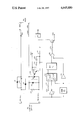
- FIGURE of the accompanying drawing is a schematic diagram of the disconnect circuit of the present invention.
- the disconnect circuit of the present invention is shown connectable between two telephone switching systems, i.e., a central office and a PABX.
- Resistor-diode network 11-13 is connectable to the central office via the TIP-CO lead.
- resistor-diode network 21-23 is connectable to the central office via the RING-CO lead.
- Resistor-diode network 11-13 is also connectable to the PABX via relay break contacts R1a and the TIP-PABX lead.
- Resistor-diode network 21-23 is connectable directly to the PABX via the RING-PABX lead.
- Diode 22 is a photodiode and it is optically coupled to phototransistor 24, both of which are included in optical coupler 20.
- the series combination of resistor 25 and capacitor 26 is connected across phototransistor 24 and resistor 27 is connected between ground and the junction of capacitor 26 and phototransistor 24. This junction is further connected to inverter 31 and retriggerable monostable multivibrator 32.
- Inverter 31 is connected to the clock (CLK) input of D-type flip-flop 33.
- the data-in (DI) input of this flip-flop is connected to a 12 volt source via resistor 34.
- the clear (CLR) input of this flip-flop is connected to the output of retriggerable monostable multivibrator 32. This output is further connected to inverter 35 which is connected to the second input of AND gate 36.
- the data-out (DO) output of D-type flip-flop 33 is connected to monostable multivibrator 37 which is further connected to the first input of AND gate 36.
- the output of AND gate 36 is connected to the base of transistor 41 via resistor 42.
- the emitter of this transistor is connected to a minus 50 volt source while the collector is connected to ground via relay R1.
- D-type flip-flop 33, montostable multivibrator 37 and retriggerable montostable multivibrator 32 are old and well known.
- the 12 volt and ground references may typically be derived voltages and represent a 12 volt difference in potential rather than actual 12 volt and ground connections.
- Inverter 31 provides a logic level 1 signal in response to being electrically connected to ground.
- This logic level 1 signal is applied to the clock (CLK) input of D-type flip-flop 33.
- a logic level 1 signal is also applied to the data-in (DI) input of this flip-flop since it is connected to the 12 volt source via resistor 34. Consequently, when the logic level 1 clock signal appears at the CLK input, the logic level 1 signal at the DI input is transferred to the data-out (DO) output of flip-flop 33.
- This logic level 1 signal causes monostable multivibrator 37 to provide an 850 millisecond pulse at its output. Thereafter, a steady logic level 0 signal appears on this output.
- This logic level 0 signal is applied to the first input of AND gate 36, causing it to provide a logic level 0 signal at its output and thereby cause transistor 41 to be turned off. Consequently, relay R1 is not operated and break contacts R1a are closed.
- This delay circuit ensures that a logic level 1 (12 volt) signal appears at the inputs of inverter 31 and retriggerable monostable multivibrator 32 only if phototransistor 24 remains turned on for a predetermined time period defined by the parameters of the delay circuit. These resistive and capacitive parameters are typically chosen to provide a 35 millisecond delay period. The delay circuit thus ensures that the disconnect circuit of the present invention ignores spurious noise pulses and responds only to interruptions in loop current having a duration of 35 milliseconds or more.
- phototransistor 24 When loop current is present for more than the predetermined 35 millisecond delay period, phototransistor 24 does gate the logic level 1 (12 volt) potential appearing at its collector input to the inputs of inverter 31 and retriggerable monostable multivibrator 32. Inverter 31 detects this logic level 1 signal and applies a logic level 0 signal to the clock (CLK) input of D-type flip-flop 33.
- Retriggerable monostable multivibrator 32 has a time period of 12 seconds and thus operates as a 12 second enable timer. Therefore this retriggerable monostable multivibrator provides a 12 second logic level 1 output signal in response to a logic level 1 (+12 volt) signal appearing at its input. Since this multivibrator is retriggerable, it re-initiates the 12 second timing period upon each appearance of a logic level 1 signal at its input. Thus, retriggerable monostable multivibrator 32 operates to inhibit the effect of interruptions in loop current caused by dial pulses since each time a dial pulse occurs multivibrator 32 is retriggered. This retriggering then initiates a new 12 second logic level 1 signal at the output of multivibrator 32.
- the output signal from this multivibrator will however return to a logic level 0 signal 12 seconds after either the last dial pulse, spurious open condition or reverse battery spike during an answering connection.
- retriggerable monostable multivibrator 32 operates to ignore such dial pulses, spurious open conditions and reverse battery spikes during answer connections.
- D-type flip-flop 33 is disabled, since this logic level 1 signal also appears at the clear (CLR) input of this flip-flop.
- CLR clear
- retriggerable monostable multivibrator 32 provides a logic level 0 signal at its output and thus the clear condition is removed from the CLR input of D-type flip-flop 33. This flip-flop is then in condition to respond to signals appearing at its clock (CLK) input of 35 milliseconds or longer duration.
- the logic level 0 signal resulting from the ground connection has no effect on retriggerable monostable multivibrator 32.
- inverter 31 responds to this logic level 0 signal by applying a logic level 1 signal to the CLK input of D-type flip-flop 33.
- This logic level 1 clock signal causes D-type flip-flop 33 to transfer the logic level 1 signal appearing at its DI input to its DO output.
- the logic level 1 signal at the DO output of D-type flip-flop 33 then appears at the input of monostable multivibrator 37.
- This multivibrator provides an 850 millisecond logic level 1 pulse in response to the logic level 1 signal at its input.
- retriggerable monostable multivibrator 32 Since retriggerable monostable multivibrator 32 has a logic level 0 signal at its input it also has a logic level 0 signal at its output. This logic level 0 output signal appears at the input of inverter 35 which then provides a logic level 1 signal at the second input of AND gate 36.
- This AND gate then gates the 850 millisecond pulse from monostable multivibrator 37 to transistor 41 via resistor 42.
- Transistor 41 then turns on for 850 milliseconds and operates relay R1 for the same period of time. Consequently, break contacts R1a are opened for this same 850 millisecond period. Thus, the loop is opened for 850 milliseconds in response to a calling party controlled disconnect signal.
- This 850 millisecond open condition gives the PABX sufficient time to disconnect an internal station from the line before the central office can connect a subsequent call to the PABX.
- this circuit gives the central office sufficient time to disconnect an internal station from the line before the PABX can connect a subsequent call to the central office.
Landscapes
- Engineering & Computer Science (AREA)
- Signal Processing (AREA)
- Interface Circuits In Exchanges (AREA)
Abstract
Description
Claims (16)
Priority Applications (4)
| Application Number | Priority Date | Filing Date | Title |
|---|---|---|---|
| US06/655,139 US4645880A (en) | 1984-09-27 | 1984-09-27 | Disconnect circuit for use between telephone switching systems |
| CA000470966A CA1233898A (en) | 1983-12-27 | 1984-12-21 | Disconnect circuit for use between telephone switching systems |
| BE2/60584A BE901380A (en) | 1984-09-27 | 1984-12-27 | DISCONNECTION CIRCUIT TO BE INTERCALED BETWEEN TELEPHONE SWITCHING SYSTEMS. |
| IT20920/85A IT1185582B (en) | 1984-09-27 | 1985-05-28 | SEPARATION CIRCUIT FOR USE BETWEEN TELEPHONE SWITCHING SYSTEMS |
Applications Claiming Priority (1)
| Application Number | Priority Date | Filing Date | Title |
|---|---|---|---|
| US06/655,139 US4645880A (en) | 1984-09-27 | 1984-09-27 | Disconnect circuit for use between telephone switching systems |
Publications (1)
| Publication Number | Publication Date |
|---|---|
| US4645880A true US4645880A (en) | 1987-02-24 |
Family
ID=24627688
Family Applications (1)
| Application Number | Title | Priority Date | Filing Date |
|---|---|---|---|
| US06/655,139 Expired - Lifetime US4645880A (en) | 1983-12-27 | 1984-09-27 | Disconnect circuit for use between telephone switching systems |
Country Status (4)
| Country | Link |
|---|---|
| US (1) | US4645880A (en) |
| BE (1) | BE901380A (en) |
| CA (1) | CA1233898A (en) |
| IT (1) | IT1185582B (en) |
Citations (4)
| Publication number | Priority date | Publication date | Assignee | Title |
|---|---|---|---|---|
| US3865993A (en) * | 1973-06-11 | 1975-02-11 | Itt | Trunk circuit with forced release feature |
| US4049919A (en) * | 1976-11-03 | 1977-09-20 | Gte Automatic Electric Laboratories Incorporated | Communication system trunk circuit |
| US4058685A (en) * | 1976-11-19 | 1977-11-15 | North Electric Company | Interoffice loop supervision arrangement |
| US4190745A (en) * | 1978-12-01 | 1980-02-26 | Gte Automatic Electric Laboratories Incorporated | Call for service and continuity sensor circuit |
-
1984
- 1984-09-27 US US06/655,139 patent/US4645880A/en not_active Expired - Lifetime
- 1984-12-21 CA CA000470966A patent/CA1233898A/en not_active Expired
- 1984-12-27 BE BE2/60584A patent/BE901380A/en not_active IP Right Cessation
-
1985
- 1985-05-28 IT IT20920/85A patent/IT1185582B/en active
Patent Citations (4)
| Publication number | Priority date | Publication date | Assignee | Title |
|---|---|---|---|---|
| US3865993A (en) * | 1973-06-11 | 1975-02-11 | Itt | Trunk circuit with forced release feature |
| US4049919A (en) * | 1976-11-03 | 1977-09-20 | Gte Automatic Electric Laboratories Incorporated | Communication system trunk circuit |
| US4058685A (en) * | 1976-11-19 | 1977-11-15 | North Electric Company | Interoffice loop supervision arrangement |
| US4190745A (en) * | 1978-12-01 | 1980-02-26 | Gte Automatic Electric Laboratories Incorporated | Call for service and continuity sensor circuit |
Also Published As
| Publication number | Publication date |
|---|---|
| IT8520920A0 (en) | 1985-05-28 |
| IT8520920A1 (en) | 1986-11-28 |
| IT1185582B (en) | 1987-11-12 |
| BE901380A (en) | 1985-04-16 |
| CA1233898A (en) | 1988-03-08 |
Similar Documents
| Publication | Publication Date | Title |
|---|---|---|
| US4700380A (en) | Solid state remote actuable switch | |
| EP0651541B1 (en) | Telephone subscriber circuit with galvanic isolating element for driving the on/off states of a telephone line | |
| US3742151A (en) | Communication call holding and supervising circuit | |
| US4056691A (en) | Telephone subscriber line circuit | |
| CA1064582A (en) | Analog timer including controllable operate-recovery time constants | |
| US4306119A (en) | Telephone outpulsing circuit | |
| US4450571A (en) | Two-way signal transmission and one-way DC power supply using a single line pair | |
| US4143287A (en) | Photo coupling line isolation circuit | |
| US3867567A (en) | Electronic data terminal interface | |
| US4645880A (en) | Disconnect circuit for use between telephone switching systems | |
| US4145577A (en) | Ringing control apparatus | |
| GB892435A (en) | Electronic switching system | |
| US4024351A (en) | Telephone line battery boost circuit | |
| US3714586A (en) | Modem carrier detecting circuit | |
| IE41228L (en) | Gaurd circuit for relay | |
| US4313037A (en) | Telephone station set with improved flash signalling | |
| US4110566A (en) | Switching network control arrangement | |
| US3838224A (en) | Electronic telephone trunk circuit | |
| US4002850A (en) | Trunk adapter | |
| US4099031A (en) | Method and apparatus for automatically identifying an individual calling party on a multiparty telephone line | |
| US5307403A (en) | Telephone branch line transmission circuit with blocking capacitor | |
| US2996680A (en) | Transistorized pulse demodulator | |
| US3879579A (en) | Automatic direct access arrangement selector | |
| US4311879A (en) | AC Supervisory signal detector circuit | |
| EP0613275B1 (en) | Driver interface for a telephone line switch enabling a speech circuit under any polarity conditions |
Legal Events
| Date | Code | Title | Description |
|---|---|---|---|
| AS | Assignment |
Owner name: GTE COMMUNICATION SYSTEMS CORPORATION NORTHLAKE, I Free format text: ASSIGNMENT OF ASSIGNORS INTEREST.;ASSIGNORS:LEMBKE, ROBERT W.;WIEBELD, HOWARD J.;REEL/FRAME:004320/0513 Effective date: 19840920 |
|
| STCF | Information on status: patent grant |
Free format text: PATENTED CASE |
|
| AS | Assignment |
Owner name: GTE FLORIDA INCORPORATED, ONE TAMPA CITY CENTER 20 Free format text: ASSIGNMENT OF ASSIGNORS INTEREST.;ASSIGNOR:GTE COMMUNICATION SYSTEMS CORPORATION;REEL/FRAME:004994/0821 Effective date: 19880811 |
|
| REMI | Maintenance fee reminder mailed | ||
| FPAY | Fee payment |
Year of fee payment: 4 |
|
| SULP | Surcharge for late payment | ||
| FPAY | Fee payment |
Year of fee payment: 8 |
|
| FPAY | Fee payment |
Year of fee payment: 12 |
|
| FEPP | Fee payment procedure |
Free format text: PAYOR NUMBER ASSIGNED (ORIGINAL EVENT CODE: ASPN); ENTITY STATUS OF PATENT OWNER: LARGE ENTITY |