US4626628A - Telephone line circuit having time-shared DTMF receivers - Google Patents
Telephone line circuit having time-shared DTMF receivers Download PDFInfo
- Publication number
- US4626628A US4626628A US06/655,128 US65512884A US4626628A US 4626628 A US4626628 A US 4626628A US 65512884 A US65512884 A US 65512884A US 4626628 A US4626628 A US 4626628A
- Authority
- US
- United States
- Prior art keywords
- receiver
- tone
- signals
- signal
- dtmf
- Prior art date
- Legal status (The legal status is an assumption and is not a legal conclusion. Google has not performed a legal analysis and makes no representation as to the accuracy of the status listed.)
- Expired - Lifetime
Links
Images


Classifications
-
- H—ELECTRICITY
- H04—ELECTRIC COMMUNICATION TECHNIQUE
- H04M—TELEPHONIC COMMUNICATION
- H04M3/00—Automatic or semi-automatic exchanges
- H04M3/005—Interface circuits for subscriber lines
-
- H—ELECTRICITY
- H04—ELECTRIC COMMUNICATION TECHNIQUE
- H04Q—SELECTING
- H04Q1/00—Details of selecting apparatus or arrangements
- H04Q1/18—Electrical details
- H04Q1/30—Signalling arrangements; Manipulation of signalling currents
- H04Q1/44—Signalling arrangements; Manipulation of signalling currents using alternate current
- H04Q1/444—Signalling arrangements; Manipulation of signalling currents using alternate current with voice-band signalling frequencies
- H04Q1/45—Signalling arrangements; Manipulation of signalling currents using alternate current with voice-band signalling frequencies using multi-frequency signalling
- H04Q1/453—Signalling arrangements; Manipulation of signalling currents using alternate current with voice-band signalling frequencies using multi-frequency signalling in which m-out-of-n signalling frequencies are transmitted
-
- H—ELECTRICITY
- H04—ELECTRIC COMMUNICATION TECHNIQUE
- H04Q—SELECTING
- H04Q3/00—Selecting arrangements
- H04Q3/42—Circuit arrangements for indirect selecting controlled by common circuits, e.g. register controller, marker
Definitions
- This invention relates generally to line circuits for use in telephone systems and more particularly to a circuit and method for time-sharing a DTMF receiver between a pair of signalling sources.
- MF multifrequency
- DTMF dual-tone multifrequency
- the central office equipment or private business exchange (PBX) core equipment includes a receiver which converts each tone pair into DC or digital signals. Appropriate combinations of these signals are used conventionally to initiate the operation of the common equipment at the central office, PBX, or electronic key system.
- PBX private business exchange
- Such a system is described in an article entitled “Vantage 48: a key system with PBX features", Telesis 1983, one, at 18.
- DTMF receivers are available for use by the subscribers.
- a subscriber requests service such as by going off-hook, a receiver is attached to his line for reception of the tones.
- the receiver On completion of the signalling, the receiver is disconnected from the line and is returned to the pool.
- DTMF receivers are pooled because they tend to be costly and the provision of a one-to-one ratio of receivers to subscriber sets would be prohibitively expensive.
- the pooling of receivers sometimes contributes to blocking within the system; this occurs when the number of subscribers wishing to use their signalling system exceeds the number of receivers available.
- the invention alleviates these difficulties by providing a circuit and a method for the time-sharing of a DTMF receiver by a pair of subscriber sets whereby the signalling originated by both subscribers is effectively monitored continuously.
- a circuit for the time-sharing of a DTMF receiver comprises a control circuit which includes means for generating timing signals.
- a DTMF receiver has an input terminal for receiving analog signals and an output terminal for providing output signals representative of the identity of the input signals.
- First and second terminals are adapted for connection to respective sources of DTMF signals.
- a pair of transmission gates are responsive to switching signals from the timing generator for alternately connecting the first and second terminals to the input terminal of the DTMF receiver whereby the signalling appearing on the first and the second terminals is effectively monitored continuously.
- the invention is embodied in a line circuit having a pair of DTMF receivers each adapted to receive DTMF signalling tones from a respective pair of subscriber lines.
- the line circuit comprises a microprocessor control circuit for switching a pair of multiplexer circuits and thus control access of the receivers to the subscriber lines in accordance with a preset procedure controlled by the microprocessor.
- Each receiver is switched between a respective pair of subscriber lines at a predetermined rate until an incoming tone is detected on at least one of the subscriber lines. In that instance, DTMF detection of the incoming tone on the connected subscriber lines is completed before the switching of the receivers to the other pair of subscriber lines is resumed. In effect, the scanning of the subscriber lines is frozen when a DTMF tone is detected on one of them and is resumed when the tone detection is complete.
- FIG. 1 is a block schematic diagram of a circuit in accordance with the invention.
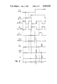
- FIG. 2 is a timing diagram illustrating the waveforms at various locations in FIG. 1;
- FIGS. 3a, 3b and 3c form a composite flow chart depicting the microprocessor instructions necessary to control the circuit of FIG. 1.
- FIG. 1 illustrates a portion of a line circuit embodying the invention.
- a processor 10 is shown connected to a buffer circuit 11 and a pair of DTMF receivers 12 and 13 via a data bus 14.
- the receivers 12 and 13 are connected to four voice frequency circuits 15 to 18 through a pair of multiplexer circuits 19 and 20 which are controlled by a signal MC from the processor 10 and by its complementary signal MC generated at the output of an inverter gate 21.
- the voice frequency interface circuits 15 to 18 are adapted to be connected to respective subscriber loops.
- Each interface circuit comprises a line coupling transformer with the primary connected to the tip and ring pair of a subscriber loop.
- the secondary windings are respectively connected to input terminals of the multiplexer circuits 19 and 20 and are identified as SS1, SS2, SS3 and SS4.
- the interface circuits 15-18 perform the usual functions of battery feed to the tip and ring terminals, loop current detection, D.C. flux cancellation in the line transformer, and ring voltage transfer and ring trip.
- the control logic hardware for the line circuit centers around the microprocessor 10 which may conveniently be an off-the-shelf unit such as model number 8749 which is equipped with read-only-memory and random-access-memory capability on the same chip.
- the processor 10 provides a UART (universal asynchronous receiver/transmitter) function for the four links and controls the functions of the line circuit such as loop detection, dial pulse and hook-switch flash decoding for four lines, ring relay control with zero crossing synchronization and ring trip detection for the four lines as well as DTMF receiver control and decoding.
- the processor obtains the information necessary to the loop detection decoding function via leads LD1, LD2, LD3 and LD4 from the interface circuits which are buffered to the data bus 14 by the circuit 11 which may also conveniently be component number 74LS244.
- Each of DTMF receivers 12 and 13 actually represents the combination of a DTMF filter--for example model number 8865--and a DTMF detector--for example, model number 8860.
- the function of the filter is to separate the high group and low group components of the composite dual tone signal and limit the resulting pair of sinewave signals to produce rectangular wave signals having the same frequencies as the individual components of the composite DTMF input.
- the high group and low group rectangular waves are applied to the detector circuit which operates thereon to determine the frequencies of the incoming tones and verify that they correspond to standard DTMF frequencies.
- a flag EST early-strobe signal
- the presence of the EST flag allows the control/discriminator to identify the detected tones to the code converter which in turn presents a four-bit binary code word corresponding to the received tone signal to an output latch.
- an StD flag is generated to indicate that the data may be read out by enabling the TOE input of the receiver.
- the time period between reception of the DTMF signals and generation of the StD flag is termed the "time to receive" and is adjustable with external components. Increasing the time to receive tends to improve the talk off performance of the receiver but degrades the response time of detection upon simultaneous incoming signals on the two lines.
- the multiplexer circuits 19 and 20 may conveniently be an off-the-shelf commercial component such as the quad multiplexer component number 14066B.
- Each half of the package provides a pair of transmission gates having their output terminals connected together and to the input terminal of a respective one of receivers 12 and 13.
- Each pair of gates is adapted to pass analog signals from one or the other of a pair of input terminals to their output terminal. Both pairs of gates are driven from the same signals MC and MC and respond thereto by connecting either of SS1 and SS3 or SS2 and SS4 to their respective DTMF receivers 12 and 13.
- the operation of the circuit may be better understood by gaining a full appreciation of the waveform illustrations of FIG. 2 and the flow chart of FIGS. 3a, 3b and 3c. Since the pair of receivers 12 and 13 and their associated multiplexing circuit operate in exactly the same way, the description of the operation will be limited to the time-sharing operation of receiver 12 between sources of DTMF signals SS1 and SS2.
- the first two waveforms of FIG. 2 illustrate the tone bursts on SS1 and SS2 input terminals; these are nominally 70 ms.
- the multiplexer circuit 19 is causing the input of the receiver 12 to be connected alternately between the input terminals SS1 and SS2 at a predetermined rate of 15 milliseconds on and off.
- a tone is present on SS2 but the SS2 gate is low (not made) and the receiver 12 does not respond.
- the tone SS2 has been connected to the input of the receiver 12 for 15 ms. and the latter responds by generating an early strobe signal EST2 which causes the scanning process of the input terminals to be frozen until the detection or reception of the SS2 tone is complete. This is acknowledged to be complete when the binary data corresponding to the tone has been received by the processor.
- the tone on SS1 arrives but without consequence since the scanning process is frozen and gate SS1 is not connected.
- the receiver generates the strobe data signal StD2 which causes the processor 10 to generate the TOE signal to cause the binary data corresponding to the tone on SS2 to be transferred to the processor 10 via the data bus 14.
- the tone SS1 is received by the receiver 12 at time L and its corresponding code read between times M and O.
- each receiver only generates one EST signal and one StD signal.
- the EST1, EST2, StD1, StD2 etc., signals are recognized by the processor because it internally associates the receiver with the scanning clock.
- the flow chart at FIGS. 3a and 3b shows timer-1 and timer-2 each one being associated with a respective process.
- FIGS. 3a and 3b illustrate graphically the operation just described.
- the Sample flag shown in the charts is used to indicate the status of the tone being received. When the Sample flag is set, it means that the tone has not been received by the receiver for 15 ms. When the Sample flag is reset, it means that no more action by the circuitry is required for the tone.
- the RD-Flag is used to indicate that the data associated with a particular tone has been read.
- the flow chart of FIG. 3c illustrates the process that the processor follows in determining whether or not the alternate switching between the two pairs of gates should take place. If terminals SS1 and SS3 are being scanned and the telephone lines associated with terminals SS2 and SS4 are inactive, that is, they are not requesting service, then switching to those terminals will be inhibited.
- the nominal duration of a DTMF tone burst is usually about seventy milliseconds. It is possible under extreme conditions that the detection of a digit may be missed by the circuitry of the invention. For this to happen, the pair of signals being time-shared by one receiver would have to occur simultaneously, be of a duration considerably shorter than normal, and the tolerance of the receiver circuitry would possibly need to be at the long end of its range. A statistical analysis indicates that the probability of these factors combining in a single circuit is very low and certainly no greater than the probability of non-detection of a digit for reasons not associated with the line circuit of the invention. As mentioned earlier, the capability of detecting shorter bursts of tones may be enhanced by decreasing the guard time of the DTMF receiver; however, decreasing the guard time is done at the expense of talk off performance.
- the time-sharing circuit and method of the invention provides a line circuit which is practical and which makes it economical to offer non-blocking DTMF monitoring service to the subscribers of a telephone system.
Landscapes
- Engineering & Computer Science (AREA)
- Computer Networks & Wireless Communication (AREA)
- Signal Processing (AREA)
- Telephonic Communication Services (AREA)
Abstract
Description
Claims (16)
Priority Applications (1)
| Application Number | Priority Date | Filing Date | Title |
|---|---|---|---|
| US06/655,128 US4626628A (en) | 1984-09-27 | 1984-09-27 | Telephone line circuit having time-shared DTMF receivers |
Applications Claiming Priority (1)
| Application Number | Priority Date | Filing Date | Title |
|---|---|---|---|
| US06/655,128 US4626628A (en) | 1984-09-27 | 1984-09-27 | Telephone line circuit having time-shared DTMF receivers |
Publications (1)
| Publication Number | Publication Date |
|---|---|
| US4626628A true US4626628A (en) | 1986-12-02 |
Family
ID=24627644
Family Applications (1)
| Application Number | Title | Priority Date | Filing Date |
|---|---|---|---|
| US06/655,128 Expired - Lifetime US4626628A (en) | 1984-09-27 | 1984-09-27 | Telephone line circuit having time-shared DTMF receivers |
Country Status (1)
| Country | Link |
|---|---|
| US (1) | US4626628A (en) |
Cited By (6)
| Publication number | Priority date | Publication date | Assignee | Title |
|---|---|---|---|---|
| US4787029A (en) * | 1986-09-29 | 1988-11-22 | Gte Communication Systems Corporation | Level converting bus extender with subsystem selection signal decoding enabling connection to microprocessor |
| US4908825A (en) * | 1988-04-08 | 1990-03-13 | Northern Telecom Limited | Memory organization and output sequencer for a signal processor |
| EP0549938A1 (en) * | 1991-12-16 | 1993-07-07 | Siemens Aktiengesellschaft | Digital message switching unit and digital message switching system |
| US5327492A (en) * | 1992-04-30 | 1994-07-05 | At&T Bell Laboratories | Method for selectively controlling the propagation of dual-tone multi-frequency signals within a telecommunications network |
| US20050180529A1 (en) * | 2002-12-31 | 2005-08-18 | Sigang Qiu | Signal detector |
| DE19844672B4 (en) * | 1998-09-29 | 2006-03-02 | Siemens Ag | Program-controlled communication system for switching connected analogue and digital communication terminals |
Citations (2)
| Publication number | Priority date | Publication date | Assignee | Title |
|---|---|---|---|---|
| US3936611A (en) * | 1974-09-04 | 1976-02-03 | Gte Sylvania Incorporated | Time compression scanner |
| US4048450A (en) * | 1974-10-25 | 1977-09-13 | Bernard Jean Michel | Trunk circuit traffic analyzer |
-
1984
- 1984-09-27 US US06/655,128 patent/US4626628A/en not_active Expired - Lifetime
Patent Citations (2)
| Publication number | Priority date | Publication date | Assignee | Title |
|---|---|---|---|---|
| US3936611A (en) * | 1974-09-04 | 1976-02-03 | Gte Sylvania Incorporated | Time compression scanner |
| US4048450A (en) * | 1974-10-25 | 1977-09-13 | Bernard Jean Michel | Trunk circuit traffic analyzer |
Cited By (6)
| Publication number | Priority date | Publication date | Assignee | Title |
|---|---|---|---|---|
| US4787029A (en) * | 1986-09-29 | 1988-11-22 | Gte Communication Systems Corporation | Level converting bus extender with subsystem selection signal decoding enabling connection to microprocessor |
| US4908825A (en) * | 1988-04-08 | 1990-03-13 | Northern Telecom Limited | Memory organization and output sequencer for a signal processor |
| EP0549938A1 (en) * | 1991-12-16 | 1993-07-07 | Siemens Aktiengesellschaft | Digital message switching unit and digital message switching system |
| US5327492A (en) * | 1992-04-30 | 1994-07-05 | At&T Bell Laboratories | Method for selectively controlling the propagation of dual-tone multi-frequency signals within a telecommunications network |
| DE19844672B4 (en) * | 1998-09-29 | 2006-03-02 | Siemens Ag | Program-controlled communication system for switching connected analogue and digital communication terminals |
| US20050180529A1 (en) * | 2002-12-31 | 2005-08-18 | Sigang Qiu | Signal detector |
Similar Documents
| Publication | Publication Date | Title |
|---|---|---|
| US4821312A (en) | Voice/data switch | |
| WO1985000487A1 (en) | Method and apparatus for sending a data message to a selected station during a silent interval between ringing | |
| US3288940A (en) | Multifrequency signal receiver | |
| US3864519A (en) | Speech-gap-responsive control apparatus | |
| US4178479A (en) | Communication processor apparatus for use in a TDM switching system | |
| US4233475A (en) | Telephone station with automatic switch-over between pulse code dialling and multifrequency code dialling | |
| ATE73974T1 (en) | DOOR TELEPHONE SYSTEM USING THE PUBLIC TELEPHONE NETWORK. | |
| US4626628A (en) | Telephone line circuit having time-shared DTMF receivers | |
| US4293737A (en) | Ringing decoder circuit | |
| CA1082826A (en) | Called party fraud detection in an automated coin system | |
| CA1220843A (en) | Digital terminal keyboard dialing | |
| US3996425A (en) | Call denial circuit | |
| CA1216690A (en) | Telephone line circuit having time-shared dtmf receivers | |
| CA1122735A (en) | Telephone station with automaticswitch-over between pulse code dialling and multifrequency code dialling | |
| US3538262A (en) | Circuit arrangement to forward dial information in exchange systems with direct distance dialling of telecommunication,particularly telephone systems | |
| US3223787A (en) | Telephone ringing control system | |
| US3536839A (en) | Answer tone detection circuit | |
| US3033932A (en) | Selective ringing multi-party telephone system | |
| US3057964A (en) | Multifrequency signaling receiver | |
| US3993875A (en) | Tone receiver | |
| EP0026020A1 (en) | Telephone set | |
| US3270143A (en) | Call-progress signal detector | |
| US3959599A (en) | Call initiation delay arrangement for digital data switching system | |
| US4370525A (en) | Variable rate timing circuit | |
| KR100206304B1 (en) | Accepting apparatus being able to process internal call for remote subscriber and the control method |
Legal Events
| Date | Code | Title | Description |
|---|---|---|---|
| AS | Assignment |
Owner name: NORTHERN TELECOM LIMITED P.O. BOX 6123 MONTEAL QUE Free format text: ASSIGNMENT OF ASSIGNORS INTEREST.;ASSIGNOR:BELL-NORTHERN RESEARCH LTD.;REEL/FRAME:004380/0160 Effective date: 19840918 Owner name: NORTHERN TELECOM LIMITED, PO BOX 6123, MONTREAL, Q Free format text: ASSIGNMENT OF ASSIGNORS INTEREST.;ASSIGNORS:NIZAMUDDIN, NADIR;YUNG, ANTHONY;REEL/FRAME:004373/0051 Effective date: 19840911 Owner name: BELL-NORTHERN RESEARCH LTD. P.O. BOX 3511 STATION Free format text: ASSIGNMENT OF ASSIGNORS INTEREST.;ASSIGNORS:RAMSARAN, JOHANN D.;BIRAY, BORA;REEL/FRAME:004373/0050 Effective date: 19840904 |
|
| STCF | Information on status: patent grant |
Free format text: PATENTED CASE |
|
| FEPP | Fee payment procedure |
Free format text: PAYOR NUMBER ASSIGNED (ORIGINAL EVENT CODE: ASPN); ENTITY STATUS OF PATENT OWNER: LARGE ENTITY |
|
| FPAY | Fee payment |
Year of fee payment: 4 |
|
| FPAY | Fee payment |
Year of fee payment: 8 |
|
| FPAY | Fee payment |
Year of fee payment: 12 |
|
| AS | Assignment |
Owner name: NORTEL NETWORKS CORPORATION, CANADA Free format text: CHANGE OF NAME;ASSIGNOR:NORTHERN TELECOM LIMITED;REEL/FRAME:010567/0001 Effective date: 19990429 |
|
| AS | Assignment |
Owner name: NORTEL NETWORKS LIMITED, CANADA Free format text: CHANGE OF NAME;ASSIGNOR:NORTEL NETWORKS CORPORATION;REEL/FRAME:011195/0706 Effective date: 20000830 Owner name: NORTEL NETWORKS LIMITED,CANADA Free format text: CHANGE OF NAME;ASSIGNOR:NORTEL NETWORKS CORPORATION;REEL/FRAME:011195/0706 Effective date: 20000830 |