US4616196A - Microwave and millimeter wave switched-line type phase shifter including exponential line portion - Google Patents
Microwave and millimeter wave switched-line type phase shifter including exponential line portion Download PDFInfo
- Publication number
- US4616196A US4616196A US06/695,523 US69552385A US4616196A US 4616196 A US4616196 A US 4616196A US 69552385 A US69552385 A US 69552385A US 4616196 A US4616196 A US 4616196A
- Authority
- US
- United States
- Prior art keywords
- transmission line
- phase shifter
- phase
- substrate
- alternate
- Prior art date
- Legal status (The legal status is an assumption and is not a legal conclusion. Google has not performed a legal analysis and makes no representation as to the accuracy of the status listed.)
- Expired - Fee Related
Links
Images


Classifications
-
- H—ELECTRICITY
- H01—ELECTRIC ELEMENTS
- H01P—WAVEGUIDES; RESONATORS, LINES, OR OTHER DEVICES OF THE WAVEGUIDE TYPE
- H01P1/00—Auxiliary devices
- H01P1/18—Phase-shifters
- H01P1/184—Strip line phase-shifters
Definitions
- the present invention relates to switched-line type phase shifters for use at microwave and millimeter wave frequencies.
- Switched-line type phase shifters can be either transmission type (two-port) or reflection type (one-port) phase shifters.
- a switched line type phase shifter which provides a selectable relative phase shift of either 0° or ⁇ ° includes two different transmission lines and a switch system for selecting either one as the transmission path to be followed by the signal to be phase shifted.
- the transmission line which constitutes the signal path when a relative phase shift of ⁇ ° is selected is made electrically longer than the transmission line which constitutes the signal path when a relative phase shift of 0° is selected.
- This difference in electrical length is selected to provide a difference in transmission time of ⁇ o seconds where ##EQU1## where T o is the period of a signal at the design operating frequency F o at which a phase shift of ⁇ ° is desired.
- T o is the period of a signal at the design operating frequency F o at which a phase shift of ⁇ ° is desired.
- F o is the operating frequency.
- the phase shift ⁇ is a function of frequency.
- phase shift provided by a switched-line type phase shifter restricts its use to narrowband systems when tight tolerances are placed on the phase shift provided.
- a switched-line type phase shifter operable over a wide frequency band includes reference and alternate transmission lines either one of which can be connected as the RF signal path through the phase shifter.
- the reference transmission line has a given phase length and a given phase versus frequency characteristic.
- the alternate transmission line includes a coupled exponential transmission line (CETL) all-pass network.
- CETL coupled exponential transmission line
- the coupled exponential transmission line which is included in the alternate transmission line has its length, line width, line separation and taper tailored to provide a phase length different from said given phase length and a phase versus frequency characteristic which substantially matches the given phase versus frequency characteristic whereby the phase shifter exhibits a substantially constant phase-versus-frequency characteristic over the operating frequency range.
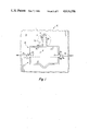
- FIG. 1 is a plan view of the strip conductor pattern of a phase shifter in accordance with the present invention
- FIG. 2 is a plot of the relative phase shift of the FIG. 1 phase shifter as a function of frequency for three different design values
- FIG. 3 is a plot of the phase shift of a coupled exponential transmission line (CETL) all pass network as a function of its electrical length with the ratio of its impedance Z oe to its impedance Z oo as a parameter.
- CETL coupled exponential transmission line
- FIG. 4 is a plot of the even and odd mode impedances of coupled microstrip transmission lines as a function of the ratio of their width to the substrate thickness for a substrate having a dielectric constant of 9.6 with the ratio of the separation between the lines to the thickness of the substrate as a parameter.
- FIG. 5 is a perspective illustration of the phase shifter structure of FIG. 1 enclosed in a waveguide to form a suspended-substrate structure.
- a phase shifter 10 in accordance with the present invention is embodied in microstrip form and comprises first and second ports 16 and 18 which are interchangeable for use as input and output ports.
- Strip transmission lines of the type having a flat broad substrate with a relatively narrow strip conductor on a face side thereof and a relatively broad ground conductor on a back side thereof are known as microstrip transmission lines.
- the relatively broad ground conductor must be at least about three times as wide as the relatively narrow strip conductor.
- the embodiment in FIG. 1 includes a dielectric substrate 12 having first and second major surfaces.
- a continuous ground conductor (not shown) is disposed on the major surface of the substrate 12 which is hidden from the plan view in FIG. 1.
- a number of individual, relatively narrow, strip conductors are disposed to form microstrip transmission lines with the dielectric substrate and ground conductor.
- One of these strip conductors 26 connects at a first end to the first port 16 and at a second end to the common terminal 27a of a single pole, double throw (SPDT) switch 27.
- SPDT single pole, double throw
- a second one of these conductive strips 28 connects at a first end to the common terminal 29a of a SPDT switch 29 and at a second end to the second port 18.
- Reference microstrip transmission line 20 and alternative microstrip transmission line 21 extend between switch 27 and switch 29.
- a strip conductor 22 comprises the relatively narrow conductor of the reference, uniform, microstrip transmission 20 line and connects at one end to the first branch terminal 27b of switch 27 and at the other end to the first branch terminal 29b of switch 29.
- a strip conductor 24 comprises the relatively narrow conductor of the alternative microstrip transmission line 21 and connects at one end to the second branch terminal 27 c of switch 27 and at the other end to the second branch terminal 29c of switch 29.
- the switches 27 and 29 are switched together so that their common contacts are both connected to their first branch terminals 27b,29b or both connected to their second branch terminals 27c, 29c to connect either the reference transmission line 20 or the alternate transmission line 21, respectively, between the ports 16 and 18.
- Reference transmission line 20 has a given phase length at a particular frequency and the increasing phase length with increasing frequency phase-versus-frequency characteristic of a uniform transmission line.
- Strip 24 includes two uniform sections 24a and 24b and two tapered sections 25a and 25b.
- the tapered sections 25a and 25b together comprise a coupled exponential transmission line (CETL) all-pass network 25.
- the conductors 25a and 25b of the CETL network 25 are widest where they connect to sections 24a and 24b, respectively and are narrowest where their ends which are remote from conductor sections 24a and 24b connect to each other.
- the length, width, spacing between and taper of the conductors of CETL 25 is tailored to provide the CETL with a phase length which is greater than that of the reference transmission line by the phase shift desired from the phase shifter and a phase-versus-frequency characteristic which is substantially the same as that of the reference transmission line over the operating range of frequencies.
- ⁇ is the rate of taper
- ⁇ l electrical length of section.
- Such a CETL section has an asymmetric phase-frequency characteristic.
- This asymmetric characteristic enables the phase shifter 10 to provide a substantially constant phase shift over a wide band.
- the phase shift characteristics of a phase shifter 10 are shown in FIG. 2 for three different design phase shift values (45°, 90° and 180°). This performance data is presented in tabular form in the Table.
- FIG. 3 is a graph of the phase shift versus ⁇ l characteristics of coupled exponential all-pass networks for selected values of ⁇ l.
- This FIGURE is copied from FIG. 10 on page 227 of an article entitled "Coupled Nonuniform Transmission Line and Its Application", by S. Yamamoto et al. which appeared in the IEEE Transactions on Microwave Theory and Techniques, Vol. MTT-15, No. 4, April 1967 at pages 220-231.
- the other curves are the characteristics of CETL networks having various values of ⁇ and ⁇ l.
- the CETL is provided with substantially the same phase-versus-frequency characteristics as the uniform line and the phase shifter itself is provided with a substantially constant phase shift versus frequency characteristic.
- phase shifters providing 45°, 90° and 180° of phase shift can be provided which have the frequency responses illustrated in FIG. 2.
- the phase shifter 10 is constructed to provide a relative phase shift of 45° between the reference transmission line and the alternate transmission line across a frequency band centered at 10 GHz.
- a characteristic impedance (Z o ) of 50 ⁇ is desired. This characteristic impedance Z o is equal to ⁇ z oe z oo
- the substrate 12 is 25 mils (0.025 inch or 0.0635 centimeter) thick alumina which has a dielectric constant of 9.6. From FIG. 2 or the Table, it can be seen that a phase shift of 45° ⁇ 2° can be obtained over an operating frequency range for which ⁇ l (the electrical length of the CETL section) has a range of 105°-132°.
- This provides a bandwidth of 0.257 octaves.
- the value of ⁇ l for the center of the band is selected as 118.5°.
- the resulting phase shifter will provide a phase shift of 45° ⁇ 2° over the frequency range from 8.86 GHz to 11.14 GHz.
- the value of ⁇ (0) is selected as 3 and the value of ⁇ l is selected as -0.5.
- From the value of ⁇ l of 118.5° at 10 GHz the desired value of l is determined to be 0.9875 centimeter. From this value of l and the selected value of ⁇ l, the desired value of ⁇ is found to be -0.50633. From the selected value of ⁇ l, P is found to be 0.7788.
- the value of p ( ⁇ l/2 ⁇ l) is -0.12088. This yields a value of q of 0.99267. From the values of ⁇ , q and l, the value of ⁇ is found to be 117.6311°. This yields a phase shift ⁇ a through the CETL section of 275.93856°. From the 45° phase shift curve in FIG. 2 it is seen that the relative phase shift provided by the phase shifter is a maximum at the center of the operating band. In consequence, in order to provide a phase shift of 45° ⁇ 2° over the operating band, the relative phase shift or ⁇ should be 47° at the center of the band.
- the relative phase shift ⁇ is equal to ( ⁇ a - ⁇ r ) where ⁇ a is the phase shift experienced by the signal when it passes through the alternate transmission line and ⁇ r is the phase shift experienced by the signal when it passes through the reference transmission line.
- the values of ⁇ a , ⁇ r , and l r are for the CETL network and its corresponding portion of the reference transmission line. Connection of an equal length of uniform transmission line in series with each of the sections does not affect the relative phase shift. Consequently, as fabricated, the switches 27 and 29 are spaced apart by a convenient distance which is normally greater than l r .
- Z oo is equal to ##EQU6## which reduces to a value of Z o / ⁇ 3 for a Z o of 50 ohms reduces to 28.8675.
- Z o is equal to ⁇ Z eo Z oo which for these values of Z oe and Z oo reduces to a value of 49.9999.
- the desired 50 ohm characteristic impedance is obtained.
- FIG. 4 is a graph of the values of Z (even) and Z (odd) of a pair of coupled microstrip transmission lines fabricated on a substrate having a dielectric constant of 9.6. This graph plots the values of Z (even) and Z (odd) as a function of w/h with s/h as a parameter where "w" is the width of both narrow strips (25a and 25b) "h” is the thickness of the substrate and "s” is the spacing of (the separation between) the two narrow strips (25a and 25b).
- FIG. 4 is copied from FIG. 7 on page 447 of an article entitled, "An Octave-Band Switched-Line Microstrip 3-b Diode Phase Shifter” by Robert P. Coats which appeared in IEEE Transactions on Microwave Theory and Techniques, Vol. MTT-21, No. 7, July 1973 at pages 444-449.
- phase shifts and operating frequency ranges can be provided by appropriate selection of the values of the design parameters of the CETL network.
- the Table shows that a 180° phase shifter using a CETL all-pass section has a bandwidth of 0.39 octave with the permissible phase error of ⁇ 2°. This characteristic is far superior to that of prior art 180° phase shifters which use a cascade of two 90° phase shift sections each containing a uniform, coupled line all-pass section.
- the switches 27 and 29 may preferably employ p-i-n type diodes to control the connection of the transmission lines.
- a first diode connects strip 22 to strip 26 and a second diode connects strip 24 to strip 26. Bias is provided to these diodes so that one is forward biased while the other is reverse biased.
- a similar connection of PIN diodes comprises switch 29.
- the phase shifter 10 is reciprocal. Consequently, its ports 16 and 18 are interchangeable and either may be connected to the source of a signal whose phase is to be switched. The other port is connected to the sink for the phase shifted signal.
- the phase shifter 10 is connected in the transmission path of the signal whose phase is to be controlled.
- the switches 27 and 29 are set to connect reference transmission line 20 between ports 16 and 18.
- the switches 27 and 29 are switched to connect the alternate transmission line 21 between the ports 16 and 18 in place of the reference transmission line.
- the CETL 25 maintains the difference in phase length between reference transmission line 20 and alternate transmission line 21 substantially constant at 45° (here ⁇ 2°) across the full designed operating frequency range of the phase shifter.
- the alternate transmission line 21 can be made a different number of degrees longer in phase length than reference transmission line 20 by appropriate modification of its design parameters.
- port 18 may be omitted and switch 29 may be replaced by reflective terminations of the transmission lines 20 and 21.
- phase shifter it is considered preferable for operational use in the millimeter wave region to form the phase shifter as a suspended-substrate structure 40 and to enclose the phase shifter structure 10 within a conductive rectangular waveguide 50 as illustrated in FIG. 5.
- the waveguide enclosure for the suspended-substrate structure prevents radiation from the transmission lines on the substrate 12 and concentrates any energy propagating through the waveguide within the transmission lines of this suspended-substrate structure.
- this suspended substrate structure it is considered preferable to omit the ground plane from the second surface of the substrate. Under such conditions, it becomes possible to place the strip conductors of the reference and alternate transmission lines on opposing surfaces of the substrate if desired. However, for ease of fabrication, it is considered preferable to place the strip conductors of both transmission lines on the same surface of the substrate.
Landscapes
- Waveguide Switches, Polarizers, And Phase Shifters (AREA)
Abstract
Description
              TABLE
______________________________________
Phase Shift  Operating range
                          Bandwidth
(degrees)    for βl(degrees)
                          (octave)
______________________________________
45° ± 2°
             105-132       0.257
90° ± 2°
             110-155      0.40
180° ± 2°
             130-180      0.39
______________________________________
Claims (5)
Priority Applications (1)
| Application Number | Priority Date | Filing Date | Title |
|---|---|---|---|
| US06/695,523 US4616196A (en) | 1985-01-28 | 1985-01-28 | Microwave and millimeter wave switched-line type phase shifter including exponential line portion |
Applications Claiming Priority (1)
| Application Number | Priority Date | Filing Date | Title |
|---|---|---|---|
| US06/695,523 US4616196A (en) | 1985-01-28 | 1985-01-28 | Microwave and millimeter wave switched-line type phase shifter including exponential line portion |
Publications (1)
| Publication Number | Publication Date |
|---|---|
| US4616196A true US4616196A (en) | 1986-10-07 |
Family
ID=24793354
Family Applications (1)
| Application Number | Title | Priority Date | Filing Date |
|---|---|---|---|
| US06/695,523 Expired - Fee Related US4616196A (en) | 1985-01-28 | 1985-01-28 | Microwave and millimeter wave switched-line type phase shifter including exponential line portion |
Country Status (1)
| Country | Link |
|---|---|
| US (1) | US4616196A (en) |
Cited By (14)
| Publication number | Priority date | Publication date | Assignee | Title |
|---|---|---|---|---|
| US4931753A (en) * | 1989-01-17 | 1990-06-05 | Ford Aerospace Corporation | Coplanar waveguide time delay shifter |
| US5073755A (en) * | 1990-03-19 | 1991-12-17 | Mpr Teltech Ltd. | Method and apparatus for measuring the electrical properties of dielectric film in the gigahertz range |
| US5116807A (en) * | 1990-09-25 | 1992-05-26 | The United States Of America As Represented By The Administrator Of The National Aeronautics And Space Administration | Monolithic MM-wave phase shifter using optically activated superconducting switches |
| US5170140A (en) * | 1988-08-11 | 1992-12-08 | Hughes Aircraft Company | Diode patch phase shifter insertable into a waveguide |
| US5789997A (en) * | 1995-06-07 | 1998-08-04 | Nokia Telecommunications Oy | Bypassable wilkinson divider |
| US5801601A (en) * | 1997-01-27 | 1998-09-01 | Lucent Technologies Inc. | Radio frequency delay line adjustment circuit |
| US5959509A (en) * | 1994-04-28 | 1999-09-28 | Alliedsignal Inc. | Printed 180 degree differential phase shifter including a non-uniform non-regular line |
| US6320481B1 (en) | 1999-06-11 | 2001-11-20 | Trw Inc. | Compact phase shifter circuit using coupled lines |
| WO2002001123A1 (en) * | 2000-06-23 | 2002-01-03 | Mmr Technologies, Inc. | Flexible counter-flow heat exchangers |
| US6989788B2 (en) * | 2002-09-16 | 2006-01-24 | Continental Microwave & Tool Co., Inc. | Antenna array having apparatus for producing time-delayed microwave signals using selectable time delay stages |
| WO2006132574A1 (en) * | 2005-06-10 | 2006-12-14 | Telefonaktiebolaget Lm Ericsson (Publ) | A phase shifter device |
| US20140152400A1 (en) * | 2012-11-30 | 2014-06-05 | Harris Corporation | Novel phase shifters and tuning elements |
| CN104810576A (en) * | 2015-03-31 | 2015-07-29 | 中国电子科技集团公司第五十五研究所 | Millimeter wave broadband 0-pi phase shifter |
| US11277123B2 (en) | 2018-05-21 | 2022-03-15 | Samsung Electronics Co., Ltd. | Method for controlling transmission of electromagnetic wave on basis of light, and device therefor |
Citations (9)
| Publication number | Priority date | Publication date | Assignee | Title |
|---|---|---|---|---|
| US3471808A (en) * | 1966-06-09 | 1969-10-07 | Itt | Phase shifter having different length conductors inserted into circuit by reed relays |
| US3568105A (en) * | 1969-03-03 | 1971-03-02 | Itt | Microstrip phase shifter having switchable path lengths |
| US3568097A (en) * | 1969-11-18 | 1971-03-02 | Texas Instruments Inc | Switched line length phase shift network for strip transmission line |
| DE2704202A1 (en) * | 1977-02-02 | 1978-08-03 | Philips Patentverwaltung | ALL-PASS ARRANGEMENT IN MICRO SLIT STRIP TECHNOLOGY |
| DE2747871A1 (en) * | 1976-11-26 | 1979-05-03 | Philips Patentverwaltung | Wide band 180 degrees phase shifter - has interleaved half and quarter wavelength meanders, using intermediate switching diodes for wavelength mode selection |
| US4195271A (en) * | 1976-11-26 | 1980-03-25 | U.S. Philips Corporation | Broad-band 180° phase shifter |
| US4238745A (en) * | 1979-06-18 | 1980-12-09 | Rca Corporation | Phase shifter |
| US4254383A (en) * | 1979-10-22 | 1981-03-03 | General Electric Company | Inverted microstrip phase shifter |
| US4383227A (en) * | 1978-11-03 | 1983-05-10 | U.S. Philips Corporation | Suspended microstrip circuit for the propagation of an odd-wave mode |
-
1985
- 1985-01-28 US US06/695,523 patent/US4616196A/en not_active Expired - Fee Related
Patent Citations (9)
| Publication number | Priority date | Publication date | Assignee | Title |
|---|---|---|---|---|
| US3471808A (en) * | 1966-06-09 | 1969-10-07 | Itt | Phase shifter having different length conductors inserted into circuit by reed relays |
| US3568105A (en) * | 1969-03-03 | 1971-03-02 | Itt | Microstrip phase shifter having switchable path lengths |
| US3568097A (en) * | 1969-11-18 | 1971-03-02 | Texas Instruments Inc | Switched line length phase shift network for strip transmission line |
| DE2747871A1 (en) * | 1976-11-26 | 1979-05-03 | Philips Patentverwaltung | Wide band 180 degrees phase shifter - has interleaved half and quarter wavelength meanders, using intermediate switching diodes for wavelength mode selection |
| US4195271A (en) * | 1976-11-26 | 1980-03-25 | U.S. Philips Corporation | Broad-band 180° phase shifter |
| DE2704202A1 (en) * | 1977-02-02 | 1978-08-03 | Philips Patentverwaltung | ALL-PASS ARRANGEMENT IN MICRO SLIT STRIP TECHNOLOGY |
| US4383227A (en) * | 1978-11-03 | 1983-05-10 | U.S. Philips Corporation | Suspended microstrip circuit for the propagation of an odd-wave mode |
| US4238745A (en) * | 1979-06-18 | 1980-12-09 | Rca Corporation | Phase shifter |
| US4254383A (en) * | 1979-10-22 | 1981-03-03 | General Electric Company | Inverted microstrip phase shifter |
Non-Patent Citations (8)
| Title |
|---|
| "An Octave-Band Switched Line Microstrip 3-b Diode Phase Shifter", R. P. Coats, IEEE Transactions on Microwave Theory and Techniques, vol. MTT-21, Jul. 1973. |
| "Broadband Diode Phase Shifter", R. V. Graver, IEEE Transactions on Microwave and Theory and Techniques, vol. MTT-20, May 1972, pp. 314-323. |
| "Coupled Non-Uniform Transmission Line and Its Applications", S. Yamamoto et al., IEEE Transactions on Microwave Theory and Techniques, vol. MTT-15, Apr. 1967, pp. 220-231. |
| An Octave Band Switched Line Microstrip 3 b Diode Phase Shifter , R. P. Coats, IEEE Transactions on Microwave Theory and Techniques, vol. MTT 21, Jul. 1973. * |
| Broadband Diode Phase Shifter , R. V. Graver, IEEE Transactions on Microwave and Theory and Techniques, vol. MTT 20, May 1972, pp. 314 323. * |
| Coupled Non Uniform Transmission Line and Its Applications , S. Yamamoto et al., IEEE Transactions on Microwave Theory and Techniques, vol. MTT 15, Apr. 1967, pp. 220 231. * |
| Schick, Burkhard & Kohler, Jurgen; "A Method of Broad Band Matching of Microstrip Differential Phase Shifters"; IEEE Transaction on MTT; vol. MTT 25, No. 8, 8/1977, pp. 666-672. |
| Schick, Burkhard & Kohler, Jurgen; A Method of Broad Band Matching of Microstrip Differential Phase Shifters ; IEEE Transaction on MTT; vol. MTT 25, No. 8, 8/1977, pp. 666 672. * |
Cited By (17)
| Publication number | Priority date | Publication date | Assignee | Title |
|---|---|---|---|---|
| US5170140A (en) * | 1988-08-11 | 1992-12-08 | Hughes Aircraft Company | Diode patch phase shifter insertable into a waveguide |
| US4931753A (en) * | 1989-01-17 | 1990-06-05 | Ford Aerospace Corporation | Coplanar waveguide time delay shifter |
| US5073755A (en) * | 1990-03-19 | 1991-12-17 | Mpr Teltech Ltd. | Method and apparatus for measuring the electrical properties of dielectric film in the gigahertz range |
| US5116807A (en) * | 1990-09-25 | 1992-05-26 | The United States Of America As Represented By The Administrator Of The National Aeronautics And Space Administration | Monolithic MM-wave phase shifter using optically activated superconducting switches |
| US5959509A (en) * | 1994-04-28 | 1999-09-28 | Alliedsignal Inc. | Printed 180 degree differential phase shifter including a non-uniform non-regular line |
| US5789997A (en) * | 1995-06-07 | 1998-08-04 | Nokia Telecommunications Oy | Bypassable wilkinson divider |
| US5801601A (en) * | 1997-01-27 | 1998-09-01 | Lucent Technologies Inc. | Radio frequency delay line adjustment circuit |
| US6320481B1 (en) | 1999-06-11 | 2001-11-20 | Trw Inc. | Compact phase shifter circuit using coupled lines |
| WO2002001123A1 (en) * | 2000-06-23 | 2002-01-03 | Mmr Technologies, Inc. | Flexible counter-flow heat exchangers |
| US6989788B2 (en) * | 2002-09-16 | 2006-01-24 | Continental Microwave & Tool Co., Inc. | Antenna array having apparatus for producing time-delayed microwave signals using selectable time delay stages |
| WO2006132574A1 (en) * | 2005-06-10 | 2006-12-14 | Telefonaktiebolaget Lm Ericsson (Publ) | A phase shifter device |
| US20080197936A1 (en) * | 2005-06-10 | 2008-08-21 | Hakan Berg | Reconfigurable Phase-Shifter |
| US7714681B2 (en) | 2005-06-10 | 2010-05-11 | Telefonaktiebolaget L M Ericsson (Publ) | Reconfigurable phase-shifter |
| US20140152400A1 (en) * | 2012-11-30 | 2014-06-05 | Harris Corporation | Novel phase shifters and tuning elements |
| US9148111B2 (en) * | 2012-11-30 | 2015-09-29 | Harris Corporation | Phase shifters and tuning elements |
| CN104810576A (en) * | 2015-03-31 | 2015-07-29 | 中国电子科技集团公司第五十五研究所 | Millimeter wave broadband 0-pi phase shifter |
| US11277123B2 (en) | 2018-05-21 | 2022-03-15 | Samsung Electronics Co., Ltd. | Method for controlling transmission of electromagnetic wave on basis of light, and device therefor |
Similar Documents
| Publication | Publication Date | Title |
|---|---|---|
| US3560893A (en) | Surface strip transmission line and microwave devices using same | |
| US4502028A (en) | Programmable two-port microwave network | |
| EP0533335B1 (en) | Radar transmitter with FET switches | |
| US4616196A (en) | Microwave and millimeter wave switched-line type phase shifter including exponential line portion | |
| US4105959A (en) | Amplitude balanced diode phase shifter | |
| US4070639A (en) | Microwave 180° phase-bit device with integral loop transition | |
| WO1995016288A1 (en) | Compact low-loss microwave balun | |
| HK1010074B (en) | Radar transmitter with fet switches | |
| US5600286A (en) | End-on transmission line-to-waveguide transition | |
| US3423699A (en) | Digital electric wave phase shifters | |
| US5116807A (en) | Monolithic MM-wave phase shifter using optically activated superconducting switches | |
| US4438415A (en) | Digital programmable attenuator | |
| US4034377A (en) | Ferrite circulators and isolators and circuits incorporating the same | |
| US5097233A (en) | Coplanar 3dB quadrature coupler | |
| EP0154958B1 (en) | Microwave radio frequency power divider/combiner | |
| US3735267A (en) | Balanced mixer | |
| US3223947A (en) | Broadband single pole multi-throw diode switch with filter providing matched path between input and on port | |
| US5412354A (en) | Single layer double ring hybrid magic-tee | |
| US4450419A (en) | Monolithic reflection phase shifter | |
| US4517535A (en) | High speed high power step attenuator method and apparatus | |
| JPH04247701A (en) | Superconductive variable phase shifter | |
| US4568893A (en) | Millimeter wave fin-line reflection phase shifter | |
| US4823096A (en) | Variable ratio power divider/combiner | |
| CA1069597A (en) | Stripline quadrature coupler | |
| US5796317A (en) | Variable impedance transmission line and high-power broadband reduced-size power divider/combiner employing same |
Legal Events
| Date | Code | Title | Description |
|---|---|---|---|
| AS | Assignment |
Owner name: RCA CORPORATION, A CORP OF DE Free format text: ASSIGNMENT OF ASSIGNORS INTEREST.;ASSIGNOR:SHARMA, ARVIND K.;REEL/FRAME:004366/0268 Effective date: 19850125 |
|
| FPAY | Fee payment |
Year of fee payment: 4 |
|
| REMI | Maintenance fee reminder mailed | ||
| AS | Assignment |
Owner name: MARTIN MARIETTA CORPORATION, MARYLAND Free format text: ASSIGNMENT OF ASSIGNORS INTEREST;ASSIGNOR:GENERAL ELECTRIC COMPANY;REEL/FRAME:007046/0736 Effective date: 19940322 |
|
| LAPS | Lapse for failure to pay maintenance fees | ||
| FP | Lapsed due to failure to pay maintenance fee |
Effective date: 19941012 |
|
| AS | Assignment |
Owner name: LOCKHEED MARTIN CORPORATION, MARYLAND Free format text: ASSIGNMENT OF ASSIGNORS INTEREST;ASSIGNOR:MARTIN MARIETTA CORPORATION;REEL/FRAME:008628/0518 Effective date: 19960128 |
|
| STCH | Information on status: patent discontinuation |
Free format text: PATENT EXPIRED DUE TO NONPAYMENT OF MAINTENANCE FEES UNDER 37 CFR 1.362 |