US4599641A - Brightness control apparatus for a video signal processing system - Google Patents
Brightness control apparatus for a video signal processing system Download PDFInfo
- Publication number
- US4599641A US4599641A US06/675,747 US67574784A US4599641A US 4599641 A US4599641 A US 4599641A US 67574784 A US67574784 A US 67574784A US 4599641 A US4599641 A US 4599641A
- Authority
- US
- United States
- Prior art keywords
- coupled
- brightness
- plural
- output
- amplifier
- Prior art date
- Legal status (The legal status is an assumption and is not a legal conclusion. Google has not performed a legal analysis and makes no representation as to the accuracy of the status listed.)
- Expired - Lifetime
Links
Images
Classifications
-
- H—ELECTRICITY
- H04—ELECTRIC COMMUNICATION TECHNIQUE
- H04N—PICTORIAL COMMUNICATION, e.g. TELEVISION
- H04N5/00—Details of television systems
- H04N5/44—Receiver circuitry for the reception of television signals according to analogue transmission standards
- H04N5/57—Control of contrast or brightness
Definitions
- This invention concerns brightness control apparatus in a video signal processing and display system wherein video output signals are AC coupled to an image display device such as a kinescope.
- plural color image representative video signals are conveyed from associated video output driver stages to respective intensity control electrodes of an image display device via plural AC signal coupling capacitors.
- An adjustable brightness control device is coupled to an input of an amplifier which is periodically keyed to operate during periodic image blanking intervals.
- a periodic output pulse from the amplifier exhibits a brightness determinative amplitude related to the setting of the brightness control.
- the brightness determinative pulse is coupled via plural separately adjustable brightness tracking controls to control inputs of video signal clamping devices respectively associated with the AC coupling capacitors.
- Brightness determinative pulses as applied to the control inputs of the clamping devices vary together in amplitude in accordance with the setting of the brightness control, and vary individually in amplitude in accordance with the settings of the tracking controls to compensate for the conduction characteristics of the image display device.
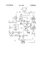
- FIGURE of the drawing shows a portion of a color video signal processing and display system such as a video monitor, including a brightness control arrangement in accordance with the principles of the present invention.
- Low level color video signals r, g and b from a source 10 are provided to respective video output driver stages 12a, 12b and 12c, which supply high level amplified color video signals R, G and B to respective cathode intensity control electrodes of a color image reproducing kinescope 18. Since driver stages 12a, 12b and 12c are identical in structure and operation, only the circuit details of red signal driver stage 12a are shown and will be discussed.
- Red color signal r is applied to the base input of an input common emitter amplifier transistor 20 which is arranged in a cascode amplifier configuration with an output common base transistor 21.
- the output circuit of transistor 21 includes a load resistor 23 coupled to a source of positive operating voltage (+v), a high frequency peaking coil 24, complementary emitter follower output buffer transistors 25 and 26, and diodes 27 and 28 which bias transistors 25 and 26 for linear conduction.
- a high level amplified red color signal R is derived from the interconnected emitter circuits of transistors 25 and 26, and is conveyed to the red kinescope cathode via an AC coupling capacitor 30a and a high frequency peaking network including a peaking coil 32 and a damping resistor 34.
- a keyed brightness control clamping network 33a included in the red video signal channel coacts with AC coupling capacitor 30a as will be discussed.
- Similar clamping networks 33b and 33c included in the green and blue video signal channels coact with associated AC coupling capacitors 30b and 30c, respectively.
- a network 40 provides brightness determinative keying pulses to clamp networks 33a, 33b and 33c.
- Network 40 includes a common emitter inverting amplifier transistor 42 with a base input electrode for receiving positive keying pulses via an input circuit including a current determining resistor 43, a speed-up circuit including the series combination of a resistor 41 and a speed-up capacitor 44 shunting resistor 43, and a manually adjustable brightness control potentiometer 45.
- Resistor 41 serves as a current limiter with respect to positive-going edge transitions of the input keying pulse as conducted by resistor 41 and capacitor 44.
- a resistor 46 assists to establish a desired brightness control range, and a resistor 47 establishes the base bias of transistor 42 together with a feedback resistor 48.
- the signal gain of the amplifier stage including transistor 42 is determined by means of feedback resistor 48 and input resistor 43.
- a waveform shaping capacitor 50 is coupled between the base input circuit and the collector output circuit of transistor 42.
- Transistor 42 is normally nonconductive and is biased for nonsaturated operation when keyed to conduct by the input keying pulse, which occurs during the relatively short "back porch" interval of each horizontal line blanking interval.
- the input keying pulse exhibits a duration of one to two microseconds and a peak-to-peak amplitude of approximately six volts, for example.
- the magnitude of a negative-going clamp keying voltage pulse produced at the inverting collector output of transistor 42 is determined by the base current of transistor 42, the magnitude of which and the conduction level of transistor 42 being related to the setting of brightness control potentiometer 45.
- the output clamp keying pulse thus exhibits a varible amplitude of, e.g., twenty to forty volts peak-to-peak amplitude as brightness control 45 is adjusted between MIN and MAX extreme settings, and is coupled via a pre-set brightness tracking potentiometer 36a for the red signal channel, a buffer transistor 37 and a coupling capacitor 38 to a cathode switching control electrode of a normally non-conductive clamp diode 35 included in clamping network 33a.
- the negative-going clamp keying pulse renders clamp diode 35 conductive whereby the charge on coupling capacitor 30a, and thereby the brightness of a displayed image, are modified in accordance with the peak amplitude of the clamp keying pulse.
- increased image brightness results when the clamp keying pulse exhibits an increased peak-to-peak amplitude, which causes a more negative voltage to be produced at the cathode of diode 35.
- the plate of capacitor 30a which is coupled to the anode of diode 35 is thereby clamped to a more negative voltage, which results in a less positive DC bias potential at the red kinescope cathode and a related increase in image brightness.
- a pre-set potentiometer 31 establishes a desired bias for clamp diode 35, and a resistor 39 coupled between the kinescope cathode signal path and a high operating potential (B+) provides a DC path for clamp diode 35.
- Pre-set adjustable brightness tracking potentiometer 36a which via the wiper thereof couples an amplitude adjusted version of the brightness determinative clamp keying pulse from the output of amplifier transistor 42 to clamp diode 35, is adjusted during system alignment to ensure proper kinescope drive ratios and white image balance for all brightness adjustment levels.
- Brightness tracking potentiometers 36b and 36c serve a similar function with respect to the green and blue signal channels. For a given change in the setting of brightness control 45 the amplitudes of the clamp keying pulses from the wipers of potentiometers 36a, 36b and 36c vary more or less depending on the settings of these controls.
- the amplitude of the clamp keying pulse at the collector of transistor 42 is approximately a linear function of the brightness control setting due to the degenerative feedback provided by resistor 48.
- the positioning of controls 36a, 36b and 36c between the output of keyed amplifier circuit 40 and clamp circuits 33a, 33b and 33c advantageously requires the use of only one keyed amplifier circuit to produce keying pulses of a level compatible with the requirements of the clamp circuits.
- the rise time of the transistor 42 collector current can be substantially reduced by means of speed-up capacitor 44.
- Capacitor 44 compensates for an otherwise unacceptably slow collector current rise time due to unavoidable small base currents which charge emitter and collector junction capacitances of transistor 42.
- the shape of the clamp keying voltage pulse at the collector of transistor 42 changes undesirably as the base current of transistor 42 is varied by means of brightness control 45.
Landscapes
- Engineering & Computer Science (AREA)
- Multimedia (AREA)
- Signal Processing (AREA)
- Processing Of Color Television Signals (AREA)
Abstract
Description
Claims (4)
Priority Applications (1)
| Application Number | Priority Date | Filing Date | Title |
|---|---|---|---|
| US06/675,747 US4599641A (en) | 1984-11-28 | 1984-11-28 | Brightness control apparatus for a video signal processing system |
Applications Claiming Priority (1)
| Application Number | Priority Date | Filing Date | Title |
|---|---|---|---|
| US06/675,747 US4599641A (en) | 1984-11-28 | 1984-11-28 | Brightness control apparatus for a video signal processing system |
Publications (1)
| Publication Number | Publication Date |
|---|---|
| US4599641A true US4599641A (en) | 1986-07-08 |
Family
ID=24711810
Family Applications (1)
| Application Number | Title | Priority Date | Filing Date |
|---|---|---|---|
| US06/675,747 Expired - Lifetime US4599641A (en) | 1984-11-28 | 1984-11-28 | Brightness control apparatus for a video signal processing system |
Country Status (1)
| Country | Link |
|---|---|
| US (1) | US4599641A (en) |
Cited By (7)
| Publication number | Priority date | Publication date | Assignee | Title |
|---|---|---|---|---|
| US4689679A (en) * | 1985-10-01 | 1987-08-25 | Rca Corporation | Brightness and automatic kinescope bias control in a video signal processor with an AC coupled kinescope driver |
| US4746973A (en) * | 1986-05-14 | 1988-05-24 | Sony Corporation | Focus block for a three-tube color video projector |
| US5057922A (en) * | 1989-09-13 | 1991-10-15 | Matsushita Electric Industrial Co., Ltd. | Black level clamping circuit including video output stage |
| US5303056A (en) * | 1992-09-14 | 1994-04-12 | Eastman Kodak Company | Dynamic gain correction for CRT printing |
| US7209183B2 (en) * | 2003-06-30 | 2007-04-24 | Samsung Electronics Co., Ltd. | Method of automatically setting image quality |
| US20100007637A1 (en) * | 2003-12-26 | 2010-01-14 | Nec Corporation | Liquid crystal display device, and method and circuit for driving for liquid crystal display device |
| US20210193764A1 (en) * | 2019-12-20 | 2021-06-24 | Samsung Display Co., Ltd. | Display device |
Citations (6)
| Publication number | Priority date | Publication date | Assignee | Title |
|---|---|---|---|---|
| US4044375A (en) * | 1976-08-19 | 1977-08-23 | Rca Corporation | Brightness control apparatus |
| US4082996A (en) * | 1976-09-27 | 1978-04-04 | Rca Corporation | Video amplifier including an a-c coupled voltage follower output stage |
| US4143398A (en) * | 1978-03-22 | 1979-03-06 | Rca Corporation | Automatic brightness control circuit employing a closed control loop stabilized against disruption by large amplitude video signals |
| US4285008A (en) * | 1978-11-15 | 1981-08-18 | Hitachi, Ltd. | Color picture reproducing device |
| EP0127439A1 (en) * | 1983-05-31 | 1984-12-05 | Burle Technologies, Inc. | Brightness control network in a video signal processor |
| US4549214A (en) * | 1983-11-07 | 1985-10-22 | Rca Corporation | Video signal DC restoration circuit |
-
1984
- 1984-11-28 US US06/675,747 patent/US4599641A/en not_active Expired - Lifetime
Patent Citations (6)
| Publication number | Priority date | Publication date | Assignee | Title |
|---|---|---|---|---|
| US4044375A (en) * | 1976-08-19 | 1977-08-23 | Rca Corporation | Brightness control apparatus |
| US4082996A (en) * | 1976-09-27 | 1978-04-04 | Rca Corporation | Video amplifier including an a-c coupled voltage follower output stage |
| US4143398A (en) * | 1978-03-22 | 1979-03-06 | Rca Corporation | Automatic brightness control circuit employing a closed control loop stabilized against disruption by large amplitude video signals |
| US4285008A (en) * | 1978-11-15 | 1981-08-18 | Hitachi, Ltd. | Color picture reproducing device |
| EP0127439A1 (en) * | 1983-05-31 | 1984-12-05 | Burle Technologies, Inc. | Brightness control network in a video signal processor |
| US4549214A (en) * | 1983-11-07 | 1985-10-22 | Rca Corporation | Video signal DC restoration circuit |
Non-Patent Citations (2)
| Title |
|---|
| Partial Schematic Circuit Diagram of Color II Video Monitor of Amdek Corp. (Oct. 1981). * |
| Partial Schematic Circuit Diagram of Color--II Video Monitor of Amdek Corp. (Oct. 1981). |
Cited By (10)
| Publication number | Priority date | Publication date | Assignee | Title |
|---|---|---|---|---|
| US4689679A (en) * | 1985-10-01 | 1987-08-25 | Rca Corporation | Brightness and automatic kinescope bias control in a video signal processor with an AC coupled kinescope driver |
| US4746973A (en) * | 1986-05-14 | 1988-05-24 | Sony Corporation | Focus block for a three-tube color video projector |
| US5057922A (en) * | 1989-09-13 | 1991-10-15 | Matsushita Electric Industrial Co., Ltd. | Black level clamping circuit including video output stage |
| US5303056A (en) * | 1992-09-14 | 1994-04-12 | Eastman Kodak Company | Dynamic gain correction for CRT printing |
| US7209183B2 (en) * | 2003-06-30 | 2007-04-24 | Samsung Electronics Co., Ltd. | Method of automatically setting image quality |
| US20100007637A1 (en) * | 2003-12-26 | 2010-01-14 | Nec Corporation | Liquid crystal display device, and method and circuit for driving for liquid crystal display device |
| US8274465B2 (en) * | 2003-12-26 | 2012-09-25 | Nlt Technologies, Ltd. | Liquid crystal display device, and method and circuit for driving for liquid crystal display device |
| US20210193764A1 (en) * | 2019-12-20 | 2021-06-24 | Samsung Display Co., Ltd. | Display device |
| US11683962B2 (en) * | 2019-12-20 | 2023-06-20 | Samsung Display Co., Ltd. | Display device having buffer transistor with control electrode in non-active area |
| US12284881B2 (en) | 2019-12-20 | 2025-04-22 | Samsung Display Co., Ltd. | Display device including buffer transistor overlapping with valley area in plan view |
Similar Documents
| Publication | Publication Date | Title |
|---|---|---|
| US4549214A (en) | Video signal DC restoration circuit | |
| CA1093206A (en) | Brightness control apparatus | |
| US4516152A (en) | Video signal processor with automatic kinescope white balance and beam current limiter control systems | |
| CA1061890A (en) | Circuit for maintaining operating point stability of an amplifier | |
| US3996609A (en) | Amplifier suitable for use as a color kinescope driver | |
| US4599641A (en) | Brightness control apparatus for a video signal processing system | |
| US4598316A (en) | Brightness control network in a video signal processor with AC coupled output stages | |
| EP0041554B1 (en) | Automatic peak beam current leveler system | |
| US4110787A (en) | Combined blanking level and kinescope bias clamp for a television signal processing system | |
| KR930004803B1 (en) | Video signal processor with automatic kinescope beam current limtter | |
| US4642690A (en) | Digital video signal processor with analog level control | |
| US4135200A (en) | Brightness control circuit with predictable brightness control range | |
| US4599651A (en) | Pulse amplifier in a brightness control system | |
| KR830002170B1 (en) | Automatic brightness control circuit | |
| US6285401B1 (en) | Apparatus for suppressing overshoots in kinescope beam current measurement pulses | |
| US4622589A (en) | Television receiver on-screen character display | |
| US4660083A (en) | Video display system with stabilized background level | |
| CA1078504A (en) | Video amplifier including an a-c coupled voltage follower output stage | |
| US4716461A (en) | Video signal blanking interval signal conditioning circuit | |
| US4641194A (en) | Kinescope driver in a digital video signal processing system | |
| US4682233A (en) | Video output signal clamping circuit | |
| US3812397A (en) | Independent electron gun bias control | |
| KR800000295B1 (en) | Operation point stabilization circuit of amplifier | |
| EP0219263B1 (en) | Video signal blanking interval signal conditioning circuit |
Legal Events
| Date | Code | Title | Description |
|---|---|---|---|
| AS | Assignment |
Owner name: RCA CORPORATION, A CORP OF DE Free format text: ASSIGNMENT OF ASSIGNORS INTEREST.;ASSIGNOR:TROIANO, ANTHONY;REEL/FRAME:004340/0489 Effective date: 19841121 Owner name: RCA CORPORATION, A CORP. OF DE,NEW JERSEY Free format text: ASSIGNMENT OF ASSIGNORS INTEREST;ASSIGNOR:TROIANO, ANTHONY;REEL/FRAME:004340/0489 Effective date: 19841121 |
|
| STCF | Information on status: patent grant |
Free format text: PATENTED CASE |
|
| AS | Assignment |
Owner name: RCA LICENSING CORPORATION, TWO INDEPENDENCE WAY, P Free format text: ASSIGNMENT OF ASSIGNORS INTEREST.;ASSIGNOR:RCA CORPORATION, A CORP. OF DE;REEL/FRAME:004993/0131 Effective date: 19871208 Owner name: RCA LICENSING CORPORATION, TWO INDEPENDENCE WAY, PRINCETON, NJ 08540, A CORP. OF DE Free format text: ASSIGNMENT OF ASSIGNORS INTEREST;ASSIGNOR:RCA CORPORATION, A CORP. OF DE;REEL/FRAME:004993/0131 Effective date: 19871208 |
|
| FPAY | Fee payment |
Year of fee payment: 4 |
|
| FPAY | Fee payment |
Year of fee payment: 8 |
|
| FPAY | Fee payment |
Year of fee payment: 12 |