US4598461A - Methods of making self-aligned power MOSFET with integral source-base short - Google Patents
Methods of making self-aligned power MOSFET with integral source-base short Download PDFInfo
- Publication number
- US4598461A US4598461A US06/693,643 US69364385A US4598461A US 4598461 A US4598461 A US 4598461A US 69364385 A US69364385 A US 69364385A US 4598461 A US4598461 A US 4598461A
- Authority
- US
- United States
- Prior art keywords
- region
- insulating layer
- source
- layer
- mask
- Prior art date
- Legal status (The legal status is an assumption and is not a legal conclusion. Google has not performed a legal analysis and makes no representation as to the accuracy of the status listed.)
- Expired - Lifetime
Links
Images


Classifications
-
- H—ELECTRICITY
- H10—SEMICONDUCTOR DEVICES; ELECTRIC SOLID-STATE DEVICES NOT OTHERWISE PROVIDED FOR
- H10D—INORGANIC ELECTRIC SEMICONDUCTOR DEVICES
- H10D30/00—Field-effect transistors [FET]
- H10D30/60—Insulated-gate field-effect transistors [IGFET]
- H10D30/64—Double-diffused metal-oxide semiconductor [DMOS] FETs
- H10D30/66—Vertical DMOS [VDMOS] FETs
-
- H—ELECTRICITY
- H10—SEMICONDUCTOR DEVICES; ELECTRIC SOLID-STATE DEVICES NOT OTHERWISE PROVIDED FOR
- H10D—INORGANIC ELECTRIC SEMICONDUCTOR DEVICES
- H10D64/00—Electrodes of devices having potential barriers
- H10D64/20—Electrodes characterised by their shapes, relative sizes or dispositions
- H10D64/23—Electrodes carrying the current to be rectified, amplified, oscillated or switched, e.g. sources, drains, anodes or cathodes
- H10D64/251—Source or drain electrodes for field-effect devices
- H10D64/252—Source or drain electrodes for field-effect devices for vertical or pseudo-vertical devices
- H10D64/2527—Source or drain electrodes for field-effect devices for vertical or pseudo-vertical devices for vertical devices wherein the source or drain electrodes are recessed in semiconductor bodies
-
- H—ELECTRICITY
- H10—SEMICONDUCTOR DEVICES; ELECTRIC SOLID-STATE DEVICES NOT OTHERWISE PROVIDED FOR
- H10D—INORGANIC ELECTRIC SEMICONDUCTOR DEVICES
- H10D64/00—Electrodes of devices having potential barriers
- H10D64/20—Electrodes characterised by their shapes, relative sizes or dispositions
- H10D64/23—Electrodes carrying the current to be rectified, amplified, oscillated or switched, e.g. sources, drains, anodes or cathodes
- H10D64/251—Source or drain electrodes for field-effect devices
- H10D64/256—Source or drain electrodes for field-effect devices for lateral devices wherein the source or drain electrodes are recessed in semiconductor bodies
-
- H—ELECTRICITY
- H10—SEMICONDUCTOR DEVICES; ELECTRIC SOLID-STATE DEVICES NOT OTHERWISE PROVIDED FOR
- H10D—INORGANIC ELECTRIC SEMICONDUCTOR DEVICES
- H10D64/00—Electrodes of devices having potential barriers
- H10D64/20—Electrodes characterised by their shapes, relative sizes or dispositions
- H10D64/27—Electrodes not carrying the current to be rectified, amplified, oscillated or switched, e.g. gates
- H10D64/311—Gate electrodes for field-effect devices
- H10D64/411—Gate electrodes for field-effect devices for FETs
- H10D64/511—Gate electrodes for field-effect devices for FETs for IGFETs
- H10D64/517—Gate electrodes for field-effect devices for FETs for IGFETs characterised by the conducting layers
- H10D64/518—Gate electrodes for field-effect devices for FETs for IGFETs characterised by the conducting layers characterised by their lengths or sectional shapes
Definitions
- the present invention relates generally to power metaloxide-semiconductor field-effect transistors (MOSFET's) manufactured by double diffusion techniques and, more particularly, to methods of manufacturing such transistors with a minimum of masking steps, methods for forming ohmic shorts between the source and base layers during the manufacture of such transistors, and transistors so manufactured.
- MOSFET's power metaloxide-semiconductor field-effect transistors
- Known power MOSFET's generally comprise a multiplicity of individual unit cells (numbering in the thousands) formed on a single silicon semiconductor wafer with each device being of the order of 300 mils (0.3 in.) square in size and all cells in each device being electrically connected in parallel. Each cell is typically between 5 and 50 microns in width.
- one particular known process for manufacturing power MOSFET's is a double diffusion technique which begins with a common drain region of, for example, N type semiconductor material. Specifically, within the drain region a base region is formed by means of a first diffusion, and then a source region is formed entirely within the base region by means of a second diffusion. If the drain region is N type, then the first diffusion is done with acceptor impurities to produce a P type base region, and the second diffusion is done with donor impurities to produce an N + type source region.
- the source, base and drain regions correspond respectively to the emitter, base and collector of a parasitic bipolar transistor.
- this parasitic bipolar transistor is allowed to turn on during operation of the power MOSFET, the blocking voltage and the dV/dt rating of the power MOSFET are substantially degraded.
- the layers comprising the source and base regions are normally shorted together by means of an ohmic connection.
- CMOS complementary metal-oxide-semiconductor
- CMOS complementary metal-oxide-semiconductor
- metallization is applied for the source electrode, and a portion of the source metallization also makes ohmic contact with the previously masked area of the base region.
- a double-diffused power MOSFET comprises individual cells formed on a semiconductor substrate including a drain region of one conductivity type, for example N type, and having a principal surface.
- a metallized drain terminal is electrically connected to the drain region, typically on the other surface thereof.
- a first region of opposite conductivity type in this example P type
- the first region is of limited lateral extent, and has a periphery terminating at the principal surface.
- a second region of the one conductivity type in this example N type is formed entirely within, and of, lesser lateral extent and depth than the base region.
- the second region has a periphery terminating at the principal surface within and spaced from the periphery of the base region such that at the principal surface the base region exists as a band of the opposite conductivity type (in this example P type semiconductor material) between the source region and the drain region, both of N type semiconductor material.
- a source terminal is electrically connected to the second region.
- a conductive gate electrode and a gate insulating layer are formed on the principal surface at least laterally over the band of the first region, and a gate terminal is electrically connected to the gate electrode.
- an ohmic short is formed between the first and second regions (base and source regions) below the principal surface.
- the source terminal comprises a metallic electrode, preferably aluminum, deposited over the source region
- the ohmic short comprises at least one microalloy spike extending from the source terminal metallic electrode through the second region and partly into the first region.
- microalloy spikes are formed by heating the semiconductor substrate after the metallic electrode has been deposited under appropriate conditions.
- a V-groove is formed by preferential etching in the source and base regions.
- the V-groove extends through the source region, with the bottom of the V-groove extending only partly into the base region.
- a metallic source electrode is deposited over the source region and into the V-groove in ohmic contact with both the source and base regions to form both the source terminal and the ohmic short.
- a method of manufacturing a double-diffused power MOSFET begins with the step of providing a silicon semiconductor wafer substrate including a drain region of one conductivity type, for example N type, having a principal surface.
- a first or gate insulating layer, a conductive gate electrode layer (for example, highly doped N + type polysilicon), a second insulating layer, and a third insulating layer are successively formed on the principal surface, the third insulating layer being the top.
- the first mask is applied over the third insulating layer with a window for ultimately defining at least one base region and at least one source region.
- openings defined by the windows in the first mask are made through at least the third insulating layer, the second insulating layer, and the conductive gate electrode layer. During the etching, undercutting of the conductive gate layer occurs.
- the first mask is then removed.
- the first introduction step defines a base region by introducing into the drain region through the openings defined by the first mask impurities appropriate to form a first region of opposite conductivity type to the drain region, for example, acceptor impurities to form P type semiconductor material.
- the lateral extent of the base region is determined in part by the size of the openings defined by this first mask, as well as by the duration of the introduction of impurities and other processing parameters.
- the source region is defined by the second impurity introduction step, which involves introducing into the base region, also through the openings defined by the first mask, impurities to form a second region of the one conductivity type (in this example, N type). Significantly, there is no need for any additional impurity barrier over any part of the base region.
- the source region is formed entirely within the base region such that at the principal surface the first region exists as a band of opposite conductivity type between the source and the drain region.
- a layer of silicon dioxide is grown at least on the sidewalls of the opening through the gate electrode layer.
- an insulating layer on the surface of the source region is removed with a collimated beam in an area defined by the opening in the third insulating layer defined by the first mask.
- the collimated beam allows this etching to proceed without removing the silicon dioxide layer on the side walls of the opening through the gate electrode layers.
- the second masking step defines gate contact areas on a portion of the device other than at the location of the source region. Using windows in the second mask, the third insulating layer and the second insulating layer are successively etched through to the polysilicon gate electrode layer. Thereafter, the second mask is removed.
- electrode metal such as aluminum is coated onto the wafer and is then patterned by means of a third mask to form source and gate electrode layers.
- the wafer is heated to form at least one microalloy spike extending from the metal source electrode through the source region and partly into the base region.
- the overall device is similarly formed, but the source-base short is formed by preferential etching to form a V-groove, and then filling the V-groove with the source electrode material in ohmic contact with both the source and base regions. More particularly, after the insulating layer on the surface of the source region is removed with a collimated beam, the second and first layers are preferentially etched to form a V-groove, the V-groove extending through the second region and the bottom of the V-groove extending only partly into the first region.
- the second mask is provided with windows for defining the gate contact area, and the third insulating layer and the second insulating layer are successively etched through to form an opening for the gate electrode.
- the second mask is removed.
- electrode metal is coated onto the wafer and is then patterned by means of a third mask to form source and gate electrode layers.
- the source layer extend into the V-groove in ohmic contact with both the second and first regions.
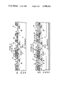
- FIG. 1 is a sectional side view depicting one step in the manufacture of a prior art double-diffused power MOSFET showing diffusion barriers for base shorting bars still in place;
- FIG. 2 is a sectional side view depicting a prior art double-diffused power MOSFET substantially completed
- FIG. 3 depicts a semiconductor wafer after initial processing to form a self-aligned pcwer MOSFET cell in accordance with the present invention
- FIG. 4 depicts the condition of the cell after a subsequent step where the top four layers have been etched through, and a first mask removed;
- FIG. 5 depicts the wafer after the base and source diffusions
- FIG. 6 depicts removal with a collimated beam of oxide grown over the source region
- FIG. 7 depicts the second masking step and the subsequent etching to expose the gate electrode
- FIG. 8 depicts metallization of source and gate electrodes applied in combination with a third masking step
- FIG. 9 depicts integral source-base shorts formed by the microalloy technique of the present invention.
- FIG. 10 depicts a V-groove formed by preferential etching in accordance with another aspect of the invention.
- FIG. 11 depicts a unit cell with an integral source-base short formed by filling the V-groove with metallization.
- FIGS. 1 and 2 It is believed that the present invention will be better understood and appreciated in view of the details of one form of prior art double-diffused power MOSFET described herein with reference to FIGS. 1 and 2.
- the prior art MOSFET manufacturing technique depicted in FIGS. 1 and 2 requires up to six masking steps which must be aligned to each other with high accuracy to produce working devices.
- a completed prior art power MOSFET comprises a multiplicity of unit cells 16, numbering in the thousands, formed in a single semiconductor wafer 18 and electrically connected in parallel on each device.
- the unit cells 16 have a common drain region 20 of N or N - type silicon semiconductor material having a common metal electrode 22 in ohmic contact through a highly doped N + substrate 24.
- the unit cells 16 have individual source 26 and base regions 28 produced by a double diffusion technique hereinafter described.
- each base region 28 exists as a band 30 of P type semiconductor material between N type source 26 and drain 20 regions.
- a metal electrode 32 covers most of the device, and makes ohmic contact with both the source 26 and base 28 regions, contact to each base region 28 being facilitated by an extension 34 of the base region 28 up to the surface of the semiconductor wafer.
- This extension 34 may be viewed as a shorting bar, and necessarily occupies surface area.
- the metal electrode 32 serves not only as a common source contact, but as the requisite source-base short.
- a conductive gate electrode 36 separated by an insulating gate oxide layer 38 is positioned on the surface 29 of the semiconductor wafer 18 at least laterally over the band 30 of P type material comprising the base region 28. While many MOSFET's include a metal gate electrode, for convenience in fabrication power MOSFET's typically employ an equivalent highly-doped and therefore highly conductive layer of polycrystalline silicon, and the name MOSFET is retained.
- the individual segments 36 of gate electrode material comprise a single perforated layer and thus are electrically connected together even though not apparent from the sectional side view of FIG. 2.
- the upper surfaces of the gate electrode segments 36 are protected by suitable insulation, for example a silicon dioxide layer 40 and a silicon nitride layer 42.
- gate contact windows 44 are provided, and metallization 46 is applied through these windows in ohmic contact with the gate electrode material 36.
- the upper surface of the completed device is essentially completely covered with metallization, except for insulating gaps 48 between the source-base metallization 32 and the gate metallization 46.
- a multiplicity of the unit cells 16 are formed, numbering in the thousands as previously stated. No particular plan view is depicted herein as a variety of known arrangements are suitable.
- the individual cells 16 may be arranged in a closely-packed hexagonal pattern, squares, or rectangular strips. While there are many thousands of unit cells 16, only a few gate contact windows 44 are provided. Due to the relatively little gate current which flows extremely low resistance to the interconnected gate electrodes is not required.
- each unit cell 16 is normally nonconducting, with a relatively high withstand voltage.
- a positive voltage is applied to the gate electrode layer 36 via the gate terminal metallization 46, an electric field is created which extends through the gate insulating layer 38 into the base region 28 and induces a thin N type conductive channel just under the surface 29 below the gate electrode 36 and insulating layer 38.
- the more positive the gate voltage the thicker this conductive channel becomes, and the more working current flows. Current flows horizontally near the surface 29 between the source 26 and drain 20 regions, and then vertically through the remaining drain region 20 and through the substrate 24 to the metal drain terminal 22.
- a typical prior art manufacturing process begins with an N/N + epitaxial wafer 18 of suitable epitaxial thickness and resistivity to support the desired voltage.
- the wafer 18 comprises the N + silicon substrate 24 approximately 15 mils thick and having a resistivity in the order of 0.01 ohm-centimeter.
- the N doped portion 20 of the wafer 18 ultimately forms a common drain region 20 of the power MOSFET.
- the wafer 18, and particularly the drain region 20, have a principal surface 29 on top of which a number of layers are successively applied.
- the gate oxide layer 38 is first grown on the surface 29 of the drain region 20 by heating in a furnace in the presence of oxygen.
- the highly-conductive polysilicon gate electrode layer 36 is deposited, which may comprise, for example, 1.1 microns of polysilicon which has been highly doped with, for example, phosphorus.
- a fine-geometry photoresist mask (not shown) is applied to define the location of the P diffusions for the base regions, and the four top layers 42, 40 36 and 38 are appropriately etched through to the surface 29 of the drain region 20.
- a P diffusion is performed, for example, three microns thick, by diffusing appropriate acceptor impurities into the drain region 20.
- a temporary oxide layer 52 is grown on the wafer surface 50 simultaneously with the P diffusion.
- a diffusion barrier comprising portions of the oxide layer 52 is formed by means of a fine-geometry photoresist mask (not shown) requiring relatively precise alignment to leave the oxide 52 which was grown during the first diffusion step only over part of the base region.
- the second diffusion step is performed by diffusing appropriate donor impurities into the base region to form the N + source regions 26.
- an oxide lip 54 is grown at the edge of the polysilicon gate electrode 36.
- a layer of silicon dioxide (not shown) is deposited over the entire surface of the wafer, and a third mask is provided for defining contact areas.
- the oxide 52 over the extension 34 of the P base region 28 to the surface is etched through, as well as the just-deposited silicon dioxide over the N + source region 26.
- the top layers 42 and 40 are also etched through to form the gate contact window 44.
- metal preferably aluminum
- the source electrode 32 makes ohmic contact with both the source region 26 and also the P base region 28 via the extension 34.
- a source-base short is provided to prevent the turn on of the parasitic bipolar transistor.
- FIGS. 3-11 depict methods in accordance with the present invention, and power MOSFET's formed thereby.
- a self-aligned double-diffused power MOSFET with integral source-base short begins with an N/N + epitaxial wafer 60 having a highly-doped N + bulk substrate 62 and an expitaxially grown drain region 64 of one conductivity type, for example, N type semiconductor, having a principal surface 66.
- a first or gate insulating layer 68 is formed and is preferably in the form of a single layer of silicon dioxide grown by heating the wafer 60 in a furnace in the presence of oxygen.
- the first insulating layer 68 could comprise, for instance, a layer of silicon dioxide grown in the foregoing manner, over which a layer of silicon nitride is deposited.
- the conductive gate electrode layer 70 which, by way of example, may comprise a 1.1 micron layer of polysilicon which has been highly doped with phosphorus to form a highly-conductive N + layer.
- the gate electrode is not actually metal, but is the electrical equivalent.
- a second insulating layer 72 preferably comprising a single layer of silicon dioxide, is formed on the polysilicon layer 70.
- the second insulating layer typically is 6 to 7 thousand angstroms thick in order to provide good dielectric isolation between a completed conductive gate layer 70 and a completed source electrode layer 102, as depicted in FIG. 9.
- the forming of the second insulating layer 72 is followed by the deposition on top of the layer 72 of a third insulating layer 74, preferably comprising a single layer of silicon nitride, or alternatively, for instance, a single layer of aluminum oxide. (The purpose served by the third insulating layer 74 is discussed below.)
- the four layers 68, 70, 72 and 74 are done consecutively, and are present everywhere on the wafer surface.
- a first mask 77 is provided over the third insulating layer 74, with windows 78 which ultimately define the source and base regions. While this first mask 77 is a relatively fine-geometry mask, no alignment is required since it is the first mask and the wafer up to this point simply comprises uniform layers. Significantly, in the process of the present invention the first mask 77 is the only fine-geometry mask.
- the third insulating layer 74, the second insulating layer 72, the conductive gate electrode layer 70, and the first insulating layer 68 are successively etched through to form respective openings 80, 82, 84, and 86 in the areas defined by the windows 78 in the first mask 77, with undercutting of the conductive gate layer 70 being necessary.
- the upper layer 74 where it comprises a single layer of silicon nitride, is plasma etched away.
- the next lower layer 72 where it comprises a single layer of silicon dioxide, is chemically etched away.
- the polysilicon layer 70 is plasma etched away with the etching continued for a sufficiently long time to produce significant sideways etching of the polysilicon layer 70 for reasons which will hereinafter be apparent. For example, in the order of 1.0 microns of undercutting is sufficient.
- the first layer 68 where it comprises a single layer of silicon dioxide, is chemically etched away. The photoresist layer 77 is then removed, leaving the wafer in the condition depicted in FIG. 4.
- the transistor base region 76 is introduced into the drain region 64, preferably by means of first a diffusion. Specifically, impurities appropriate to form a first region of opposite conductivity type are diffused into the drain region 64 through the openings 80, 82, 84 and 86 defined by the first mask 77. In this example, acceptor impurities are diffused to provide P type semiconductor material for the base region 77.
- the first diffusion to form the base region 76 is, for example, approximately 3 microns deep.
- the lateral extent of the base region 76 is determined in part by the size of the openings 80, 82, 84 and 86 defined by the first mask 77, as well as by the other process parameters, such as duration, temperature and pressure.
- the base diffusion region 76 has a periphery 79 terminating at the principal surface 66.
- the transistor source region 88 is introduced into the base region 76, preferably by means of a second diffusion step. More particularly, through the same openings 80, 82, 84, and 86 impurities appropriate to form a second diffused region 88 of the one conductivity type are introduced, in this example, donor impurities to form a highly-doped N + type semiconductor source region 88.
- This second diffusion is in the order of 1.0 micron deep, and is formed entirely within and has lesser lateral extent and depth than the base region 76 formed during the first diffusion.
- the base region 76 exists as a band 90 of the opposite conductivity type (P type) between the source region 88 (N + type) and the drain region 64 (N - type).
- a layer 92 of silicon dioxide is grown over the surface of the source region 88, and an extension 94 of this layer 92 is grown on the sidewalls 84 of the polysilicon gate electrode 70.
- the wafer exists as depicted in FIG. 5.
- the oxide layer 92 (FIG. 5) on the surface of the source region 88 is removed preferably by reactive ion etching, or, alternatively, for example, by ion milling, with a collimated beam 95 having a high selectivity ratio for silicon dioxide over silicon.
- the wafer is excited by an RF source which causes oscillatory movement of the etching ions perpendicular to the wafer surface so that a directional effect results.
- the top or third layer 74 serves to protect the top surface of the MOSFET being formed, with the edge of the window 80 providing a shadow mask.
- the silicon dioxide layer 92 on the sidewalls 84 of the polysilicon gate 70 is not removed.
- a second photoresist mask 96 is applied for the purpose of defining the gate contact opening window.
- the third insulating layer 74 at least where it comprises silicon nitride, is plasma etched away and the second insulating layer 72, is chemically etched away to form openings 98 and 100 for the gate contact window.
- the second mask 96 is then removed, and the wafer cleaned.
- electrode metal preferably aluminum
- evaporation a coating of a metal onto the device and patterned as at 102 and 104 to form source and gate electrode layers.
- This patterning requires the third mask in the preferred process of the present invention.
- a common drain electrode 105 is also metallized onto the substrate 62, but requires no patterning.
- microalloy spikes 103 are produced, which extend all the way through the source diffusion layer 88 and partly into the base diffusion 76. It will be appreciated that the precise process parameters must be selected to produce the desired results. However, by way of example, without intending to limit the scope of the invention, for an N + source layer 88 which is less than about 0.7 microns thick, heating at 450° C. for one hour in a nitrogen atmosphere is sufficient to cause the desired degree of microalloying.
- the silicon of the source 88 and base 76 layers dissolves in the aluminum source contact 102, allowing the microalloy spikes 103 to form downwardly.
- the extent of the microalloying can be varied by controlling a number of parameters, for example
- a second technique for forming a source-base short in a power MOSFET which involved employing known preferential etching techniques to form a V-groove.
- processing proceeds as described above beginning with FIG. 3 up through FIG. 6.
- the wafer substrate 60 is selected to have the particular crystallographic orientation of ⁇ 100>.
- the source and base diffused regions 88 and 76 are preferentially etched to form a V-groove 106, the V-groove 106 extending all the way through the source region 88 with the bottom 108 of the V-groove 106 extending only partly into the base region 76.
- a suitable etchant is a mixture of potassium hydroxide and isopropanol in a ratio of approximately 3:1. This particular etching mixture etches silicon at a rate of 5 microns per hour when the mixture is maintained at approximately 60° C. Other orientation-dependent etches may also be used in practicing the invention.
- suitable etchant such as a aqueous KOH solution.
- the second mask is applied, such as the mask 96 depicted above with reference to FIG. 7, and the gate contact windows 98 and 100 are formed. This second mask 96 is then removed.
- metal is coated, preferably by evaporation, onto the device and patterned to form source and electrode layers, as described above with reference to FIG. 8.
- the source electrode 102 is in ohmic contact with both the source 88 and base 76 regions.
- source and drain electrode layers of the power MOSFET described above could be formed by a coating process comprising sputtering in contrast to evaporation, as described above. It is therefore to be understood that the appended claims are intended to cover the foregoing and all such modifications as fall within the true spirit and scope of the invention.
Landscapes
- Insulated Gate Type Field-Effect Transistor (AREA)
- Electrodes Of Semiconductors (AREA)
Abstract
Description
Claims (19)
Priority Applications (1)
| Application Number | Priority Date | Filing Date | Title |
|---|---|---|---|
| US06/693,643 US4598461A (en) | 1982-01-04 | 1985-01-22 | Methods of making self-aligned power MOSFET with integral source-base short |
Applications Claiming Priority (2)
| Application Number | Priority Date | Filing Date | Title |
|---|---|---|---|
| US33697282A | 1982-01-04 | 1982-01-04 | |
| US06/693,643 US4598461A (en) | 1982-01-04 | 1985-01-22 | Methods of making self-aligned power MOSFET with integral source-base short |
Related Parent Applications (1)
| Application Number | Title | Priority Date | Filing Date |
|---|---|---|---|
| US06/579,229 Division US4516143A (en) | 1982-01-04 | 1984-02-13 | Self-aligned power MOSFET with integral source-base short and methods of making |
Publications (1)
| Publication Number | Publication Date |
|---|---|
| US4598461A true US4598461A (en) | 1986-07-08 |
Family
ID=26990479
Family Applications (1)
| Application Number | Title | Priority Date | Filing Date |
|---|---|---|---|
| US06/693,643 Expired - Lifetime US4598461A (en) | 1982-01-04 | 1985-01-22 | Methods of making self-aligned power MOSFET with integral source-base short |
Country Status (1)
| Country | Link |
|---|---|
| US (1) | US4598461A (en) |
Cited By (24)
| Publication number | Priority date | Publication date | Assignee | Title |
|---|---|---|---|---|
| US4682405A (en) * | 1985-07-22 | 1987-07-28 | Siliconix Incorporated | Methods for forming lateral and vertical DMOS transistors |
| US4755482A (en) * | 1986-02-19 | 1988-07-05 | Kabushiki Kaisha Toshiba | Making semiconductor device on insulating substrate by forming conductive layers on both major surfaces |
| US4760432A (en) * | 1985-11-04 | 1988-07-26 | Siemens Aktiengesellschaft | Thyristor having controllable emitter-base shorts |
| US4866492A (en) * | 1986-02-28 | 1989-09-12 | Polyfet Rf Devices, Inc. | Low loss fet |
| US4879254A (en) * | 1987-06-10 | 1989-11-07 | Nippondenso Co., Ltd. | Method of manufacturing a DMOS |
| US4898835A (en) * | 1988-10-12 | 1990-02-06 | Sgs-Thomson Microelectronics, Inc. | Single mask totally self-aligned power MOSFET cell fabrication process |
| US4920064A (en) * | 1986-08-08 | 1990-04-24 | U.S. Philips Corporation | Method of manufacturing an insulated gate field effect transistor DMOS |
| US5032532A (en) * | 1987-08-24 | 1991-07-16 | Hitachi, Ltd. | Method for fabricating insulated gate semiconductor device |
| US5047117A (en) * | 1990-09-26 | 1991-09-10 | Micron Technology, Inc. | Method of forming a narrow self-aligned, annular opening in a masking layer |
| US5084418A (en) * | 1988-12-27 | 1992-01-28 | Texas Instruments Incorporated | Method of making an array device with buried interconnects |
| US5179034A (en) * | 1987-08-24 | 1993-01-12 | Hitachi, Ltd. | Method for fabricating insulated gate semiconductor device |
| US5223732A (en) * | 1991-05-28 | 1993-06-29 | Motorola, Inc. | Insulated gate semiconductor device with reduced based-to-source electrode short |
| US5256583A (en) * | 1986-03-21 | 1993-10-26 | Advanced Power Technology, Inc. | Mask surrogate semiconductor process with polysilicon gate protection |
| US5528063A (en) * | 1993-11-12 | 1996-06-18 | Calogic Corporation | Conductive-overlaid self-aligned MOS-gated semiconductor devices |
| US5573837A (en) * | 1992-04-22 | 1996-11-12 | Micron Technology, Inc. | Masking layer having narrow isolated spacings and the method for forming said masking layer and the method for forming narrow isolated trenches defined by said masking layer |
| US5731604A (en) * | 1994-09-01 | 1998-03-24 | International Rectifier Corporation | Semiconductor device MOS gated |
| EP0901161A3 (en) * | 1997-09-03 | 1999-10-06 | Siliconix Incorporated | Planar DMOS transistor fabricated by a three mask process |
| US6153473A (en) * | 1997-12-12 | 2000-11-28 | National Semiconductor Corporation | Method of symmetrically implanted punch-through stopper for a rugged DMOS power device |
| US6624030B2 (en) * | 2000-12-19 | 2003-09-23 | Advanced Power Devices, Inc. | Method of fabricating power rectifier device having a laterally graded P-N junction for a channel region |
| US6649973B2 (en) * | 2001-03-28 | 2003-11-18 | Rohm Co., Ltd. | Semiconductor device and method for manufacturing the same |
| US6724039B1 (en) * | 1998-08-31 | 2004-04-20 | Stmicroelectronics, Inc. | Semiconductor device having a Schottky diode |
| US20070181886A1 (en) * | 2006-02-09 | 2007-08-09 | Nissan Motor., Ltd. | Semiconductor device |
| US20100052046A1 (en) * | 2005-07-25 | 2010-03-04 | Fairchild Semiconductor Corporation | Semiconductor structures formed on substrates and methods of manufacturing the same |
| USRE42864E1 (en) * | 2001-09-07 | 2011-10-25 | Ixys Corporation | Rugged and fast power MOSFET and IGBT |
Citations (12)
| Publication number | Priority date | Publication date | Assignee | Title |
|---|---|---|---|---|
| US3845495A (en) * | 1971-09-23 | 1974-10-29 | Signetics Corp | High voltage, high frequency double diffused metal oxide semiconductor device |
| US3988761A (en) * | 1970-02-06 | 1976-10-26 | Sony Corporation | Field-effect transistor and method of making the same |
| US4181542A (en) * | 1976-10-25 | 1980-01-01 | Nippon Gakki Seizo Kabushiki Kaisha | Method of manufacturing junction field effect transistors |
| US4219835A (en) * | 1978-02-17 | 1980-08-26 | Siliconix, Inc. | VMOS Mesa structure and manufacturing process |
| US4271424A (en) * | 1977-06-09 | 1981-06-02 | Fujitsu Limited | Electrical contact connected with a semiconductor region which is short circuited with the substrate through said region |
| US4344081A (en) * | 1980-04-14 | 1982-08-10 | Supertex, Inc. | Combined DMOS and a vertical bipolar transistor device and fabrication method therefor |
| US4345265A (en) * | 1980-04-14 | 1982-08-17 | Supertex, Inc. | MOS Power transistor with improved high-voltage capability |
| US4417385A (en) * | 1982-08-09 | 1983-11-29 | General Electric Company | Processes for manufacturing insulated-gate semiconductor devices with integral shorts |
| US4430792A (en) * | 1982-07-08 | 1984-02-14 | General Electric Company | Minimal mask process for manufacturing insulated-gate semiconductor devices with integral shorts |
| US4443931A (en) * | 1982-06-28 | 1984-04-24 | General Electric Company | Method of fabricating a semiconductor device with a base region having a deep portion |
| US4466176A (en) * | 1982-08-09 | 1984-08-21 | General Electric Company | Process for manufacturing insulated-gate semiconductor devices with integral shorts |
| US4516143A (en) * | 1982-01-04 | 1985-05-07 | General Electric Company | Self-aligned power MOSFET with integral source-base short and methods of making |
-
1985
- 1985-01-22 US US06/693,643 patent/US4598461A/en not_active Expired - Lifetime
Patent Citations (12)
| Publication number | Priority date | Publication date | Assignee | Title |
|---|---|---|---|---|
| US3988761A (en) * | 1970-02-06 | 1976-10-26 | Sony Corporation | Field-effect transistor and method of making the same |
| US3845495A (en) * | 1971-09-23 | 1974-10-29 | Signetics Corp | High voltage, high frequency double diffused metal oxide semiconductor device |
| US4181542A (en) * | 1976-10-25 | 1980-01-01 | Nippon Gakki Seizo Kabushiki Kaisha | Method of manufacturing junction field effect transistors |
| US4271424A (en) * | 1977-06-09 | 1981-06-02 | Fujitsu Limited | Electrical contact connected with a semiconductor region which is short circuited with the substrate through said region |
| US4219835A (en) * | 1978-02-17 | 1980-08-26 | Siliconix, Inc. | VMOS Mesa structure and manufacturing process |
| US4344081A (en) * | 1980-04-14 | 1982-08-10 | Supertex, Inc. | Combined DMOS and a vertical bipolar transistor device and fabrication method therefor |
| US4345265A (en) * | 1980-04-14 | 1982-08-17 | Supertex, Inc. | MOS Power transistor with improved high-voltage capability |
| US4516143A (en) * | 1982-01-04 | 1985-05-07 | General Electric Company | Self-aligned power MOSFET with integral source-base short and methods of making |
| US4443931A (en) * | 1982-06-28 | 1984-04-24 | General Electric Company | Method of fabricating a semiconductor device with a base region having a deep portion |
| US4430792A (en) * | 1982-07-08 | 1984-02-14 | General Electric Company | Minimal mask process for manufacturing insulated-gate semiconductor devices with integral shorts |
| US4417385A (en) * | 1982-08-09 | 1983-11-29 | General Electric Company | Processes for manufacturing insulated-gate semiconductor devices with integral shorts |
| US4466176A (en) * | 1982-08-09 | 1984-08-21 | General Electric Company | Process for manufacturing insulated-gate semiconductor devices with integral shorts |
Non-Patent Citations (2)
| Title |
|---|
| Kendall, Applied Physics Letters, "On Etching Very Narrow Grooves in Silicon", vol. 26, No. 4, Feb. 15, 1975, pp. 195-198. |
| Kendall, Applied Physics Letters, On Etching Very Narrow Grooves in Silicon , vol. 26, No. 4, Feb. 15, 1975, pp. 195 198. * |
Cited By (28)
| Publication number | Priority date | Publication date | Assignee | Title |
|---|---|---|---|---|
| US4682405A (en) * | 1985-07-22 | 1987-07-28 | Siliconix Incorporated | Methods for forming lateral and vertical DMOS transistors |
| US4760432A (en) * | 1985-11-04 | 1988-07-26 | Siemens Aktiengesellschaft | Thyristor having controllable emitter-base shorts |
| US4755482A (en) * | 1986-02-19 | 1988-07-05 | Kabushiki Kaisha Toshiba | Making semiconductor device on insulating substrate by forming conductive layers on both major surfaces |
| US4866492A (en) * | 1986-02-28 | 1989-09-12 | Polyfet Rf Devices, Inc. | Low loss fet |
| US5256583A (en) * | 1986-03-21 | 1993-10-26 | Advanced Power Technology, Inc. | Mask surrogate semiconductor process with polysilicon gate protection |
| US4920064A (en) * | 1986-08-08 | 1990-04-24 | U.S. Philips Corporation | Method of manufacturing an insulated gate field effect transistor DMOS |
| US4879254A (en) * | 1987-06-10 | 1989-11-07 | Nippondenso Co., Ltd. | Method of manufacturing a DMOS |
| US5032532A (en) * | 1987-08-24 | 1991-07-16 | Hitachi, Ltd. | Method for fabricating insulated gate semiconductor device |
| US5179034A (en) * | 1987-08-24 | 1993-01-12 | Hitachi, Ltd. | Method for fabricating insulated gate semiconductor device |
| US4898835A (en) * | 1988-10-12 | 1990-02-06 | Sgs-Thomson Microelectronics, Inc. | Single mask totally self-aligned power MOSFET cell fabrication process |
| US5084418A (en) * | 1988-12-27 | 1992-01-28 | Texas Instruments Incorporated | Method of making an array device with buried interconnects |
| US5047117A (en) * | 1990-09-26 | 1991-09-10 | Micron Technology, Inc. | Method of forming a narrow self-aligned, annular opening in a masking layer |
| US5223732A (en) * | 1991-05-28 | 1993-06-29 | Motorola, Inc. | Insulated gate semiconductor device with reduced based-to-source electrode short |
| US5573837A (en) * | 1992-04-22 | 1996-11-12 | Micron Technology, Inc. | Masking layer having narrow isolated spacings and the method for forming said masking layer and the method for forming narrow isolated trenches defined by said masking layer |
| US5663079A (en) * | 1993-11-12 | 1997-09-02 | Calogic Corporation | Method of making increased density MOS-gated semiconductor devices |
| US5798549A (en) * | 1993-11-12 | 1998-08-25 | Calogic Corporation | Conductive layer overlaid self-aligned MOS-gated semiconductor devices |
| US5528063A (en) * | 1993-11-12 | 1996-06-18 | Calogic Corporation | Conductive-overlaid self-aligned MOS-gated semiconductor devices |
| US5731604A (en) * | 1994-09-01 | 1998-03-24 | International Rectifier Corporation | Semiconductor device MOS gated |
| EP0901161A3 (en) * | 1997-09-03 | 1999-10-06 | Siliconix Incorporated | Planar DMOS transistor fabricated by a three mask process |
| US6153473A (en) * | 1997-12-12 | 2000-11-28 | National Semiconductor Corporation | Method of symmetrically implanted punch-through stopper for a rugged DMOS power device |
| US6724039B1 (en) * | 1998-08-31 | 2004-04-20 | Stmicroelectronics, Inc. | Semiconductor device having a Schottky diode |
| US6624030B2 (en) * | 2000-12-19 | 2003-09-23 | Advanced Power Devices, Inc. | Method of fabricating power rectifier device having a laterally graded P-N junction for a channel region |
| US6765264B1 (en) | 2000-12-19 | 2004-07-20 | Advanced Power Devices | Method of fabricating power rectifier device to vary operating parameters and resulting device |
| US6649973B2 (en) * | 2001-03-28 | 2003-11-18 | Rohm Co., Ltd. | Semiconductor device and method for manufacturing the same |
| USRE42864E1 (en) * | 2001-09-07 | 2011-10-25 | Ixys Corporation | Rugged and fast power MOSFET and IGBT |
| US20100052046A1 (en) * | 2005-07-25 | 2010-03-04 | Fairchild Semiconductor Corporation | Semiconductor structures formed on substrates and methods of manufacturing the same |
| US20070181886A1 (en) * | 2006-02-09 | 2007-08-09 | Nissan Motor., Ltd. | Semiconductor device |
| US7714352B2 (en) * | 2006-02-09 | 2010-05-11 | Nissan Motor Co., Ltd. | Hetero junction semiconductor device |
Similar Documents
| Publication | Publication Date | Title |
|---|---|---|
| US4598461A (en) | Methods of making self-aligned power MOSFET with integral source-base short | |
| US4417385A (en) | Processes for manufacturing insulated-gate semiconductor devices with integral shorts | |
| US4466176A (en) | Process for manufacturing insulated-gate semiconductor devices with integral shorts | |
| US4516143A (en) | Self-aligned power MOSFET with integral source-base short and methods of making | |
| US6498071B2 (en) | Manufacture of trench-gate semiconductor devices | |
| US4682405A (en) | Methods for forming lateral and vertical DMOS transistors | |
| EP0342952B1 (en) | Topographic pattern delineated power MOSFET with profile tailored recessed source | |
| US5119153A (en) | Small cell low contact resistance rugged power field effect devices and method of fabrication | |
| US4384301A (en) | High performance submicron metal-oxide-semiconductor field effect transistor device structure | |
| US6274437B1 (en) | Trench gated power device fabrication by doping side walls of partially filled trench | |
| EP0777910B1 (en) | Process for manufacture of mos gated device with reduced mask count | |
| US6043126A (en) | Process for manufacture of MOS gated device with self aligned cells | |
| US5019522A (en) | Method of making topographic pattern delineated power MOSFET with profile tailored recessed source | |
| US5182234A (en) | Profile tailored trench etch using a SF6 -O2 etching composition wherein both isotropic and anisotropic etching is achieved by varying the amount of oxygen | |
| US4430792A (en) | Minimal mask process for manufacturing insulated-gate semiconductor devices with integral shorts | |
| US6660591B2 (en) | Trench-gate semiconductor devices having a channel-accommodating region and their methods of manufacture | |
| US4561168A (en) | Method of making shadow isolated metal DMOS FET device | |
| CA1197023A (en) | Self-aligned power mosfet with integral source-base short and methods of making | |
| EP0996969B1 (en) | Manufacture of trench-gate semiconductor devices | |
| EP0227894A2 (en) | High density vertical DMOS transistor | |
| US5234851A (en) | Small cell, low contact assistance rugged power field effect devices and method of fabrication | |
| KR100272051B1 (en) | P-channel MOS gate device fabrication process through base injection through contact window | |
| US5256583A (en) | Mask surrogate semiconductor process with polysilicon gate protection | |
| EP0996970B1 (en) | Manufacture of field-effect semiconductor devices | |
| JPH0363210B2 (en) |
Legal Events
| Date | Code | Title | Description |
|---|---|---|---|
| FEPP | Fee payment procedure |
Free format text: PAYOR NUMBER ASSIGNED (ORIGINAL EVENT CODE: ASPN); ENTITY STATUS OF PATENT OWNER: LARGE ENTITY |
|
| STCF | Information on status: patent grant |
Free format text: PATENTED CASE |
|
| FPAY | Fee payment |
Year of fee payment: 4 |
|
| FEPP | Fee payment procedure |
Free format text: PAYOR NUMBER ASSIGNED (ORIGINAL EVENT CODE: ASPN); ENTITY STATUS OF PATENT OWNER: LARGE ENTITY Free format text: PAYER NUMBER DE-ASSIGNED (ORIGINAL EVENT CODE: RMPN); ENTITY STATUS OF PATENT OWNER: LARGE ENTITY |
|
| FPAY | Fee payment |
Year of fee payment: 8 |
|
| FPAY | Fee payment |
Year of fee payment: 12 |
|
| AS | Assignment |
Owner name: INTERSIL CORPORATION, FLORIDA Free format text: ASSIGNMENT OF ASSIGNORS INTEREST;ASSIGNOR:HARRIS CORPORATION;REEL/FRAME:010255/0405 Effective date: 19990813 |
|
| AS | Assignment |
Owner name: CREDIT SUISSE FIRST BOSTON, AS COLLATERAL AGENT, N Free format text: SECURITY INTEREST;ASSIGNOR:INTERSIL CORPORATION;REEL/FRAME:010351/0410 Effective date: 19990813 |
|
| AS | Assignment |
Owner name: INTERSIL HOLDING CORPORATION, CALIFORNIA Free format text: INTELLECTUAL PROPERTY PARTIAL RELEASE;ASSIGNOR:CREIDT SUISSE FIRST BOSTON;REEL/FRAME:011667/0166 Effective date: 20010303 |
|
| AS | Assignment |
Owner name: FAIRCHILD SEMICONDUCTOR CORPORATION, MAINE Free format text: REASSIGNMENT OF PATENT APPLICATIONS;ASSIGNOR:INTERSIL CORPORATION;REEL/FRAME:012002/0206 Effective date: 20010406 |
|
| AS | Assignment |
Owner name: SEMICONDUCTOR COMPONENTS INDUSTRIES, LLC, ARIZONA Free format text: ASSIGNMENT OF ASSIGNORS INTEREST;ASSIGNOR:FAIRCHILD SEMICONDUCTOR CORPORATION;REEL/FRAME:057694/0374 Effective date: 20210722 |