US4545113A - Process for fabricating a lateral transistor having self-aligned base and base contact - Google Patents
Process for fabricating a lateral transistor having self-aligned base and base contact Download PDFInfo
- Publication number
- US4545113A US4545113A US06/527,146 US52714683A US4545113A US 4545113 A US4545113 A US 4545113A US 52714683 A US52714683 A US 52714683A US 4545113 A US4545113 A US 4545113A
- Authority
- US
- United States
- Prior art keywords
- layer
- polycrystalline silicon
- metal silicide
- impurity
- conductivity type
- Prior art date
- Legal status (The legal status is an assumption and is not a legal conclusion. Google has not performed a legal analysis and makes no representation as to the accuracy of the status listed.)
- Expired - Lifetime
Links
Images

Classifications
-
- H—ELECTRICITY
- H10—SEMICONDUCTOR DEVICES; ELECTRIC SOLID-STATE DEVICES NOT OTHERWISE PROVIDED FOR
- H10D—INORGANIC ELECTRIC SEMICONDUCTOR DEVICES
- H10D10/00—Bipolar junction transistors [BJT]
- H10D10/311—Thin-film BJTs
-
- H10P32/302—
-
- H10P76/40—
Definitions
- This invention relates to a lateral transistor structure and to processes for fabricating it, and in particular to a lateral transistor structure having a self-aligned base/base contact and a very narrow base width compared to existing lateral transistors.
- the maximum switching frequency for such transistors has been limited by primarily two parameters--the total base resistance and the collector-base capacitance. Nonetheless using three micron integrated circuit layout rules these parameters have been low enough to permit switching speeds on the order of 1 to 3 nanoseconds. As integrated circuit processing technology moves closer to permitting 1 micron layout rules, very shallow junctions, and very narrow base widths, it is expected that transistors may usefully operate at frequencies of up to 10 gigaHertz. At such high frequencies switching performance will be almost completely dependent upon base resistance and collector-base capacitance.
- transistors are well known. Different techniques of integrated circuit manufacture have been used to fabricate such transistors. One well known technique is to use a double diffusion process, for example, as taught by Schinella and Anthony in U.S. Pat. Nos. 3,919,005 or 3,945,857. Using this process, the transistor base is created by laterally and vertically diffusing into an epitaxial semiconductor layer formed over a buried layer, a base impurity of the desired conductivity type. Much of the base is then counter doped with a second diffusion of opposite conductivity type for the emitter or collector of the transistor.
- a double diffusion process for example, as taught by Schinella and Anthony in U.S. Pat. Nos. 3,919,005 or 3,945,857.
- the transistor base is created by laterally and vertically diffusing into an epitaxial semiconductor layer formed over a buried layer, a base impurity of the desired conductivity type. Much of the base is then counter doped with a second diffusion of opposite conductivity type for the emitter or collector of
- the second diffusion overdopes all but a narrow portion of the base impurity, resulting in the base width of the transistor being that portion of the structure not overdoped by the second diffusion.
- the semiconductor substrate forms the other of the collector or emitter. Contact to the base is made by the buried layer, while contact to the buried layer is made elsewhere by a doped region extending through the epitaxial layer to the buried layer. The doped region is the same conductivity type as the buried layer.
- a second technique for fabricating lateral transistors in integrated circuit structures has been to deposit a line of masking material on the surface of an epitaxial layer and then diffuse impurities for the collector and emitter toward each other in the substrate from opposite sides of the line.
- the base region will be the portion of the epitaxial layer between the diffusion fronts of the emitter and the collector. Electrical contact to the base is made through a buried layer.
- All of the above techniques suffer from several disadvantages. Each technique, because of the buried layer and the need to make electrical contact to it, creates a transistor structure which occupies an undesirably large area on the wafer. None of the techniques allows sufficient control over the processes involved to achieve base widths less than 1 micron. Further, diffusing the collector-emitter impurities for even slightly too long will overdope the semiconductor material which would other-wise form the base, and destroy the function of the transistor.
- This invention provides a lateral transistor structure having a self-aligned base/base contact and a narrower base width than present lateral transistors.
- the narrower base allows virtually all of the electrons injected by the emitter to be transported across the base to the collector, and reduces the transit time for the injected electrons. This increases the speed at which the transistor may change states.
- Transistors fabricated according to this invention may have base widths on the order of 2,000 to 5,000 angstroms, switch in less than 100 picoseconds, and have collector-base capacitances on the order of 0.001 picofarads.
- the integrated circuit structure of the invention includes an insulating substrate, a semiconductor layer of first conductivity type on the substrate, the semiconductor layer having a region of opposite conductivity type therein extending through the layer, and a conductive region overlying substantially all of the region of opposite conductivity and none of the first conductivity type.
- the region of opposite conductivity type will divide the semiconductor layer into two non-contiguous regions of first conductivity type, and an insulating region will surround the conductive region except where the conductive region contacts the region of opposite conductivity type.
- the semiconductor layer will be doped with N conductivity type impurity, while the conductive material will include a lower layer of doped polycrystalline silicon and an upper layer of a metal silicide.
- a method of fabricating the structure includes the steps of forming a first layer on an underlying semiconductor substrate, and forming a second layer on the first layer, the second layer having an edge; defining a zone of impurity in the second layer by introducing a first impurity into the second layer through the edge; removing the first layer except where it is overlaid by the zone of impurity; and introducing a second impurity into the substrate except where the substrate is overlaid by the first layer.
- each of the first and the second layers themselves will be made up of two or more layers. To describe these embodiments the individual layers within either the first or second layers will be referred to as "regions", although as will be explained each region may be a layer.
- the underlying semiconductor substrate is P conductivity type silicon
- the first layer itself comprises three regions formed atop each other--a first region of polycrystalline silicon disposed directly on the semiconductor substrate, a region of a metal silicide formed upon the surface of the polycrystalline silicon, and a first region of silicon dioxide formed atop the metal silicide.
- the second layer which is formed upon the surface of the first layer also comprises a sandwich type structure including a second region of polycrystalline silicon and a second region of silicon dioxide.
- five successive regions are formed on the semiconductor substrate; from bottom to top being polycrystalline silicon, a metal silicide, silicon dioxide, a second layer of polycrystalline silicon, and a second layer of silicon dioxide.
- an edge in the second layer (the polycrystalline-silicon dioxide sandwich) is defined by a masking and chemical etching procedure.
- the second region of polycrystalline silicon is exposed only along this edge, with its upper surface being protected by the second region of silicon dioxide and its lower surface being protected by the first layer.
- a suitable impurity is then laterally diffused into the exposed edge of the second region of polycrystalline silicon to define the zone of impurity.
- a selective etchant all of the second region of silicon dioxide and the second region of polycrystalline silicon are removed, except for that portion of the second region of polycrystalline silicon doped by the laterally diffused impurity.
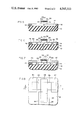
- FIG. 1 is a cross-sectional view of a semicondutor substrate after formation of the first and second layers.
- FIG. 2 shows the same cross-section after definition of an edge in the second layer.
- FIG. 3 shows a subsequent cross-section after removal of all of the second layer except the doped portion.
- FIG. 4 shows a subsequent cross-section after using the second layer as a mask for removal of a portion of the first layer.
- FIG. 5 shows a subsequent cross-section after removal of all of the first layer except for that portion underlying the doped portion of the second layer.
- FIG. 6 shows a subsequent cross-section after formation of oxide along the edges of the remaining first layer.
- FIG. 7 shows a subsequent cross-section after formation of electrical contacts to the emitter and collector.
- Fig. 8 is a top view of the structure shown in FIG. 7.
- FIG. 1 is a cross-sectional view of an integrated circuit structure 10 which may be fabricated using well known techniques.
- a layer of semiconductor material 14 is formed on an insulating substrate 12 .
- Insulating substrate 12 may be any material which is not electrically conductive, and in one embodiment is a silicon dioxide layer formed on the upper surface of other semiconductor materials (not shown).
- Layer 14 will typically be monocrystalline silicon. Using known masking and etching techniques, for example, as taught by Peltzer in U.S. Pat. No. 3,648,125, regions 16 of epitaxial layer 14 are converted to silicon dioxide.
- layer 14 is uniformly doped with P-conductivity type impurity, for example, boron at a concentration of 10 17 atoms per cubic centimeter.
- P-conductivity type impurity for example, boron at a concentration of 10 17 atoms per cubic centimeter.
- layer 14 is 5,000 angstroms thick and is formed using any known technique, for example, silicon on sapphire deposition or by depositing polycrystalline silicon on silicon dioxide and then laser annealing to form single crystal silicon.
- a first region of polycrystalline silicon 21 is deposited.
- Silicon layer 21 will typically be 3000 angstroms thick and formed by chemical vapor deposition processing.
- P+ impurity is then implanted in polycrystalline silicon 21, for example, using boron at a concentration of 10 20 atoms per cubic centimeter. Such implantation typically will be shallow, for example, being performed at 20 to 30 kev.
- a metal silicide 23 for example tungsten silicide, is formed by chemical vapor deposition.
- Layer 26 will be approximately 1000 angstroms thick and fabricated by thermal oxidation of silicide 23, for example, at a temperature between 800° C., and 1000° C., or by vapor deposition of silicon dioxide.
- a second region 30 of polycrystalline silicon is formed on silicon dioxide 26 . This layer will be approximately 3000 angstroms thick and formed using the same process as region 21.
- a region of silicon dioxide 33 is formed on the upper surface of the second polycrystalline silicon region 30, a region of silicon dioxide 33 is formed. This layer typically will be 2000 angstroms thick and formed by oxidizing polycrystalline silicon 30 at a temperature of 1000° C. for one hour.
- the structure in FIG. 2 may be obtained from that shown in FIG. 1.
- the first mask will define an edge 37 in silicon dioxide layer 33 and polycrystalline silicon layer 30.
- edge 37 will be used to define one edge of the base region of the lateral transistor to be formed in P-type silicon region 17.
- suitable impurities 39 for example boron are diffused laterally into layer 30. This may be accomplished using a well-known diffusion process carried out at a temperature of approximately 1000° C.
- the boron 39 will dope the polycrystalline silicon 30 to an impurity concentration of 10 20 atoms per cubic centimeter. Because silicon dioxide layers 26 and 33 are relatively impervious to impurity diffusion, the boron 39 will diffuse into layer 30 and create a doped region 41.
- the diffusion front of impurity 39 in layer 30 is designated by dashed line 43 in FIG. 2.
- a substantial advantage of the invention is that the lateral position of front 43 with respect to edge 37 may be precisely controlled. For example, at a temperature of 1000° C.
- the diffusion front 43 will advance at a rate of approximately 1 micron per hour.
- This relatively slow advance of front 43 permits extremely accurate control of the width of the doped region 41 in layer 30.
- region 41 will be between 2,000 and 5,000 angstroms wide.
- accurate control of the width of doped region 41 permits accurate control of the width of the electrical connection to the base of the lateral transistor, and correspondingly, accurate control of the width of the base of the lateral transistor.
- Oxide layer 33 and the regions of silicon layer 30 not doped by impurity 39 are next removed.
- Oxide layer 33 may be removed using conventional photolithographic technology and then an etchant, typically 10 parts water, 1 part hydrofluoric acid. This solution will also partially or completely remove the oxide layer 26 on the left side of doped polycrystalline silicon 41 not protected by overlying region 30. Removal of part or all of layer 26 will not affect the final structure because any remaining portions of the layer 26 are later removed anyway (See FIG. 4).
- the undoped portions of layer 30 may be removed using a known chemically selective etchant which attacks the undoped portions of layer 30 but not the doped portion 41.
- the structure which results after removal of oxide 33 and the undoped portions of layer 30 is shown in FIG. 3.
- the result of the process sequence through this step has been to create a region of doped polysilicon 41 having a precisely controlled width W as shown.
- oxide 26 is then used as a mask for removal of oxide 26.
- oxide 26 is removed using a known plasma etch process having parameters suitable for removing a layer of silicon dioxide approximately 1000 angstroms thick. The appearance of the structure after removal of the exposed oxide 26 is shown in FIG.
- FIG. 4 The structure of FIG. 4 is then further plasma etched to remove the exposed silicide 23 and the thereby exposed portions of the first region of polycrystalline silicon 21.
- a suitable plasma process for accomplishing this is the known planar plasma etching process.
- edges 37 and 43 will be defined in the regions 21 and 23. These edges are shown by the dashed lines in FIG. 5.
- the resulting structure is then chemically etched, for example, with a mixture of hydrofluoric and nitric acids, to undercut silicon dioxide layer 26, creating overhanging regions 38 and 44. This structure is depicted in FIG. 5. An overhang of 1000 angstroms has been found suitable.
- a layer of silicon dioxide, comprising regions 48 and 49 is then grown across the surface of the silicon layer 14, including any portion of the P-type region 17.
- layer 48 is 1000 angstroms thick and is formed by heating the structure shown in FIG. 5 in an atmosphere containing oxygen to a temperature of 1000° C. for 30 minutes. This oxidation process will also create regions 49 shown in FIG. 6, because the exposed edges of silicon region 21 will also oxidize.
- a plasma etch using a planar plasma etching procedure may then be used to remove the undesired portions 48 of the silicon dioxide. During this process, silicon dioxide layer 26 will serve as a mask to present the removal of oxide regions 49.
- N+ conductivity type impurities for example phosphorus
- regions 52 and 55 have impurity concentrations of approximately 10 20 atoms per cubic centimeter.
- electrical connections 54 and 57 may be provided to the N+ type regions 52 and 55.
- Such connections may be fabricated using aluminum, alloys of aluminum with copper and/or silicon, or with other known integrated circuit metal systems, for example, tungsten-titanium alloys.
- the surface of the structure shown in FIG. 7 may be protected by forming a layer of vapor deposited silicon dioxide (not shown), or other suitable passivating material across its upper surface.
- FIG. 8 is a top view of the structure shown in FIG. 7 with corresponding elements given the same reference numerals.
- Region 61 also metal, is used to make an electrical connection to the doped polycrystalline silicon base contact 21 by electrically connecting to silicide layer 23. That is, in FIG. 8, the region designated 23 has had the overlying oxide 26 removed to enable metal 61 to directly contact silicide 23.
- the lateral transistor structure of this invention offers several advantages over existing structures.
- the structure provides a very narrow base having a self-aligned base contact. This eliminates the need for a buried layer and for a doped region to provide a connection between the buried layer and the surface of the integrated circuit.
- the substantial size reduction in the resulting lateral bipolar transistor allows higher packing densities and lower cost.
- the elimination of any extrinsic base region (the base contact is formed over substantially all of the base) allows faster operating speeds.
- the intrinsic base resistance is very small because the width of the emitter may be determined by the thickness of the epitaxial silicon layer 14. Layers such as layer 14 may be readily fabricated less than 1 micron thick.
- the area of the intrinsic base-collector junction is also small because this area depends upon the thickness of layer 14.
- the base width of the resulting structure is accurately controllable because the extent of the lateral diffusion of P dopants in the polycrystalline layer 30 may be accurately controlled.
- the method of fabricating a lateral transistor described above provides several advantages over existing methods of fabricating such transistors. For example, only two masks are required prior to depositing metal and defining interconnections. The self-aligning electrical contact to the base region, the base region itself, and the PN junctions between the collector and base and between the emitter and base are all formed independent of alignment tolerances.
- the structure of the invention may be fabricated using any method for defining a narrow base.
- One such alternate technique is to use known electron beam mask making apparatus or to expose photoresist directly on the wafer with an electron beam.
Landscapes
- Bipolar Transistors (AREA)
Abstract
Description
Claims (10)
Priority Applications (1)
| Application Number | Priority Date | Filing Date | Title |
|---|---|---|---|
| US06/527,146 US4545113A (en) | 1980-10-23 | 1983-08-29 | Process for fabricating a lateral transistor having self-aligned base and base contact |
Applications Claiming Priority (2)
| Application Number | Priority Date | Filing Date | Title |
|---|---|---|---|
| US19977180A | 1980-10-23 | 1980-10-23 | |
| US06/527,146 US4545113A (en) | 1980-10-23 | 1983-08-29 | Process for fabricating a lateral transistor having self-aligned base and base contact |
Related Parent Applications (1)
| Application Number | Title | Priority Date | Filing Date |
|---|---|---|---|
| US19977180A Division | 1980-10-23 | 1980-10-23 |
Publications (1)
| Publication Number | Publication Date |
|---|---|
| US4545113A true US4545113A (en) | 1985-10-08 |
Family
ID=26895135
Family Applications (1)
| Application Number | Title | Priority Date | Filing Date |
|---|---|---|---|
| US06/527,146 Expired - Lifetime US4545113A (en) | 1980-10-23 | 1983-08-29 | Process for fabricating a lateral transistor having self-aligned base and base contact |
Country Status (1)
| Country | Link |
|---|---|
| US (1) | US4545113A (en) |
Cited By (15)
| Publication number | Priority date | Publication date | Assignee | Title |
|---|---|---|---|---|
| US4740478A (en) * | 1987-01-30 | 1988-04-26 | Motorola Inc. | Integrated circuit method using double implant doping |
| US4748103A (en) * | 1986-03-21 | 1988-05-31 | Advanced Power Technology | Mask-surrogate semiconductor process employing dopant protective region |
| US4837176A (en) * | 1987-01-30 | 1989-06-06 | Motorola Inc. | Integrated circuit structures having polycrystalline electrode contacts and process |
| US5019525A (en) * | 1987-08-18 | 1991-05-28 | Texas Instruments Incorporated | Method for forming a horizontal self-aligned transistor |
| US5039621A (en) * | 1990-06-08 | 1991-08-13 | Texas Instruments Incorporated | Semiconductor over insulator mesa and method of forming the same |
| US5067002A (en) * | 1987-01-30 | 1991-11-19 | Motorola, Inc. | Integrated circuit structures having polycrystalline electrode contacts |
| US5073506A (en) * | 1991-02-14 | 1991-12-17 | Allied-Signal Inc. | Method for making a self-aligned lateral bipolar SOI transistor |
| US5102812A (en) * | 1989-11-09 | 1992-04-07 | Bell Communications Research | Method of making a lateral bipolar heterojunction structure |
| US5136344A (en) * | 1988-11-02 | 1992-08-04 | Universal Energy Systems, Inc. | High energy ion implanted silicon on insulator structure |
| US5242844A (en) * | 1983-12-23 | 1993-09-07 | Sony Corporation | Semiconductor device with polycrystalline silicon active region and method of fabrication thereof |
| US5395775A (en) * | 1993-07-02 | 1995-03-07 | Siemens Aktiengesellschaft | Method for manufacturing lateral bipolar transistors |
| US5407843A (en) * | 1993-07-02 | 1995-04-18 | Siemens Aktiengesellschaft | Method for manufacturing lateral bipolar transistors |
| US5460982A (en) * | 1993-07-02 | 1995-10-24 | Siemens Aktiengesellschaft | Method for manufacturing lateral bipolar transistors |
| US7745301B2 (en) | 2005-08-22 | 2010-06-29 | Terapede, Llc | Methods and apparatus for high-density chip connectivity |
| US8957511B2 (en) | 2005-08-22 | 2015-02-17 | Madhukar B. Vora | Apparatus and methods for high-density chip connectivity |
Citations (12)
| Publication number | Priority date | Publication date | Assignee | Title |
|---|---|---|---|---|
| US3484662A (en) * | 1965-01-15 | 1969-12-16 | North American Rockwell | Thin film transistor on an insulating substrate |
| US3598664A (en) * | 1964-12-29 | 1971-08-10 | Texas Instruments Inc | High frequency transistor and process for fabricating same |
| US3648125A (en) * | 1971-02-02 | 1972-03-07 | Fairchild Camera Instr Co | Method of fabricating integrated circuits with oxidized isolation and the resulting structure |
| US3660732A (en) * | 1971-02-08 | 1972-05-02 | Signetics Corp | Semiconductor structure with dielectric and air isolation and method |
| US3739238A (en) * | 1969-09-24 | 1973-06-12 | Tokyo Shibaura Electric Co | Semiconductor device with a field effect transistor |
| US3890632A (en) * | 1973-12-03 | 1975-06-17 | Rca Corp | Stabilized semiconductor devices and method of making same |
| US3919005A (en) * | 1973-05-07 | 1975-11-11 | Fairchild Camera Instr Co | Method for fabricating double-diffused, lateral transistor |
| US3945857A (en) * | 1974-07-01 | 1976-03-23 | Fairchild Camera And Instrument Corporation | Method for fabricating double-diffused, lateral transistors |
| US4109272A (en) * | 1975-07-04 | 1978-08-22 | Siemens Aktiengesellschaft | Lateral bipolar transistor |
| US4124933A (en) * | 1974-05-21 | 1978-11-14 | U.S. Philips Corporation | Methods of manufacturing semiconductor devices |
| US4298402A (en) * | 1980-02-04 | 1981-11-03 | Fairchild Camera & Instrument Corp. | Method of fabricating self-aligned lateral bipolar transistor utilizing special masking techniques |
| US4329706A (en) * | 1979-03-01 | 1982-05-11 | International Business Machines Corporation | Doped polysilicon silicide semiconductor integrated circuit interconnections |
-
1983
- 1983-08-29 US US06/527,146 patent/US4545113A/en not_active Expired - Lifetime
Patent Citations (12)
| Publication number | Priority date | Publication date | Assignee | Title |
|---|---|---|---|---|
| US3598664A (en) * | 1964-12-29 | 1971-08-10 | Texas Instruments Inc | High frequency transistor and process for fabricating same |
| US3484662A (en) * | 1965-01-15 | 1969-12-16 | North American Rockwell | Thin film transistor on an insulating substrate |
| US3739238A (en) * | 1969-09-24 | 1973-06-12 | Tokyo Shibaura Electric Co | Semiconductor device with a field effect transistor |
| US3648125A (en) * | 1971-02-02 | 1972-03-07 | Fairchild Camera Instr Co | Method of fabricating integrated circuits with oxidized isolation and the resulting structure |
| US3660732A (en) * | 1971-02-08 | 1972-05-02 | Signetics Corp | Semiconductor structure with dielectric and air isolation and method |
| US3919005A (en) * | 1973-05-07 | 1975-11-11 | Fairchild Camera Instr Co | Method for fabricating double-diffused, lateral transistor |
| US3890632A (en) * | 1973-12-03 | 1975-06-17 | Rca Corp | Stabilized semiconductor devices and method of making same |
| US4124933A (en) * | 1974-05-21 | 1978-11-14 | U.S. Philips Corporation | Methods of manufacturing semiconductor devices |
| US3945857A (en) * | 1974-07-01 | 1976-03-23 | Fairchild Camera And Instrument Corporation | Method for fabricating double-diffused, lateral transistors |
| US4109272A (en) * | 1975-07-04 | 1978-08-22 | Siemens Aktiengesellschaft | Lateral bipolar transistor |
| US4329706A (en) * | 1979-03-01 | 1982-05-11 | International Business Machines Corporation | Doped polysilicon silicide semiconductor integrated circuit interconnections |
| US4298402A (en) * | 1980-02-04 | 1981-11-03 | Fairchild Camera & Instrument Corp. | Method of fabricating self-aligned lateral bipolar transistor utilizing special masking techniques |
Cited By (16)
| Publication number | Priority date | Publication date | Assignee | Title |
|---|---|---|---|---|
| US5242844A (en) * | 1983-12-23 | 1993-09-07 | Sony Corporation | Semiconductor device with polycrystalline silicon active region and method of fabrication thereof |
| US4748103A (en) * | 1986-03-21 | 1988-05-31 | Advanced Power Technology | Mask-surrogate semiconductor process employing dopant protective region |
| US4837176A (en) * | 1987-01-30 | 1989-06-06 | Motorola Inc. | Integrated circuit structures having polycrystalline electrode contacts and process |
| US4740478A (en) * | 1987-01-30 | 1988-04-26 | Motorola Inc. | Integrated circuit method using double implant doping |
| US5067002A (en) * | 1987-01-30 | 1991-11-19 | Motorola, Inc. | Integrated circuit structures having polycrystalline electrode contacts |
| US5019525A (en) * | 1987-08-18 | 1991-05-28 | Texas Instruments Incorporated | Method for forming a horizontal self-aligned transistor |
| US5136344A (en) * | 1988-11-02 | 1992-08-04 | Universal Energy Systems, Inc. | High energy ion implanted silicon on insulator structure |
| US5102812A (en) * | 1989-11-09 | 1992-04-07 | Bell Communications Research | Method of making a lateral bipolar heterojunction structure |
| US5039621A (en) * | 1990-06-08 | 1991-08-13 | Texas Instruments Incorporated | Semiconductor over insulator mesa and method of forming the same |
| US5162882A (en) * | 1990-06-08 | 1992-11-10 | Texas Instruments Incorporated | Semiconductor over insulator mesa |
| US5073506A (en) * | 1991-02-14 | 1991-12-17 | Allied-Signal Inc. | Method for making a self-aligned lateral bipolar SOI transistor |
| US5395775A (en) * | 1993-07-02 | 1995-03-07 | Siemens Aktiengesellschaft | Method for manufacturing lateral bipolar transistors |
| US5407843A (en) * | 1993-07-02 | 1995-04-18 | Siemens Aktiengesellschaft | Method for manufacturing lateral bipolar transistors |
| US5460982A (en) * | 1993-07-02 | 1995-10-24 | Siemens Aktiengesellschaft | Method for manufacturing lateral bipolar transistors |
| US7745301B2 (en) | 2005-08-22 | 2010-06-29 | Terapede, Llc | Methods and apparatus for high-density chip connectivity |
| US8957511B2 (en) | 2005-08-22 | 2015-02-17 | Madhukar B. Vora | Apparatus and methods for high-density chip connectivity |
Similar Documents
| Publication | Publication Date | Title |
|---|---|---|
| US4481706A (en) | Process for manufacturing integrated bi-polar transistors of very small dimensions | |
| US4503598A (en) | Method of fabricating power MOSFET structure utilizing self-aligned diffusion and etching techniques | |
| US4693782A (en) | Fabrication method of semiconductor device | |
| US4545113A (en) | Process for fabricating a lateral transistor having self-aligned base and base contact | |
| US3461360A (en) | Semiconductor devices with cup-shaped regions | |
| EP0052038B1 (en) | Method of fabricating integrated circuit structure | |
| US4425379A (en) | Polycrystalline silicon Schottky diode array | |
| US4647958A (en) | Bipolar transistor construction | |
| EP0051534A2 (en) | A method of fabricating a self-aligned integrated circuit structure using differential oxide growth | |
| US3945857A (en) | Method for fabricating double-diffused, lateral transistors | |
| EP0147249B1 (en) | Method of manufacturing transistor structures having junctions bound by insulating layers, and resulting structures | |
| US4803174A (en) | Bipolar transistor integrated circuit and method of manufacturing the same | |
| US4631568A (en) | Bipolar transistor construction | |
| US4244001A (en) | Fabrication of an integrated injection logic device with narrow basewidth | |
| JPS5936432B2 (en) | Manufacturing method of semiconductor device | |
| US4713355A (en) | Bipolar transistor construction | |
| US4628339A (en) | Polycrystalline silicon Schottky diode array | |
| EP0122004A2 (en) | Improved bipolar transistor construction | |
| US4717680A (en) | Fabrication of vertical NPN and PNP bipolar transistors in monolithic substrate | |
| EP0036499B1 (en) | A polysilicon-base self-aligned bipolar transistor process | |
| KR910000020B1 (en) | Manufacturing Method of Semiconductor Device | |
| US5629554A (en) | Semiconductor device with a bipolar transistor formed in a layer of semiconductor material provided on an insulating substrate | |
| US4200878A (en) | Method of fabricating a narrow base-width bipolar device and the product thereof | |
| US3649882A (en) | Diffused alloyed emitter and the like and a method of manufacture thereof | |
| US4609414A (en) | Emitter finger structure in a switching transistor |
Legal Events
| Date | Code | Title | Description |
|---|---|---|---|
| AS | Assignment |
Owner name: FAIRCHILD CAMERA AND INSTRUMENT CORPORATION, 464 E Free format text: ASSIGNMENT OF ASSIGNORS INTEREST.;ASSIGNOR:VORA, MADHUKAR B.;REEL/FRAME:004426/0910 Effective date: 19850709 |
|
| STCF | Information on status: patent grant |
Free format text: PATENTED CASE |
|
| FEPP | Fee payment procedure |
Free format text: PAYOR NUMBER ASSIGNED (ORIGINAL EVENT CODE: ASPN); ENTITY STATUS OF PATENT OWNER: LARGE ENTITY |
|
| FPAY | Fee payment |
Year of fee payment: 4 |
|
| FEPP | Fee payment procedure |
Free format text: PAYER NUMBER DE-ASSIGNED (ORIGINAL EVENT CODE: RMPN); ENTITY STATUS OF PATENT OWNER: LARGE ENTITY Free format text: PAYOR NUMBER ASSIGNED (ORIGINAL EVENT CODE: ASPN); ENTITY STATUS OF PATENT OWNER: LARGE ENTITY |
|
| FPAY | Fee payment |
Year of fee payment: 8 |
|
| AS | Assignment |
Owner name: NATIONAL SEMICONDUCTOR CORPORATION, CALIFORNIA Free format text: ASSIGNMENT OF ASSIGNORS INTEREST;ASSIGNOR:FAIRCHILD SEMICONDUCTOR CORPORATION;REEL/FRAME:008059/0846 Effective date: 19960726 |
|
| FEPP | Fee payment procedure |
Free format text: PAYER NUMBER DE-ASSIGNED (ORIGINAL EVENT CODE: RMPN); ENTITY STATUS OF PATENT OWNER: LARGE ENTITY Free format text: PAYOR NUMBER ASSIGNED (ORIGINAL EVENT CODE: ASPN); ENTITY STATUS OF PATENT OWNER: LARGE ENTITY |
|
| FPAY | Fee payment |
Year of fee payment: 12 |