US4512954A - Crystal growing apparatus - Google Patents
Crystal growing apparatus Download PDFInfo
- Publication number
- US4512954A US4512954A US06/521,826 US52182683A US4512954A US 4512954 A US4512954 A US 4512954A US 52182683 A US52182683 A US 52182683A US 4512954 A US4512954 A US 4512954A
- Authority
- US
- United States
- Prior art keywords
- crystal
- melt
- electrode
- crucible
- pulling
- Prior art date
- Legal status (The legal status is an assumption and is not a legal conclusion. Google has not performed a legal analysis and makes no representation as to the accuracy of the status listed.)
- Expired - Lifetime
Links
- 239000013078 crystal Substances 0.000 title claims abstract description 76
- 239000000155 melt Substances 0.000 claims abstract description 36
- 239000002994 raw material Substances 0.000 claims abstract description 19
- 238000001514 detection method Methods 0.000 claims abstract description 6
- 238000010438 heat treatment Methods 0.000 claims abstract description 4
- HBMJWWWQQXIZIP-UHFFFAOYSA-N silicon carbide Chemical compound [Si+]#[C-] HBMJWWWQQXIZIP-UHFFFAOYSA-N 0.000 claims description 10
- 229910010271 silicon carbide Inorganic materials 0.000 claims description 10
- 238000000034 method Methods 0.000 description 9
- XUIMIQQOPSSXEZ-UHFFFAOYSA-N Silicon Chemical compound [Si] XUIMIQQOPSSXEZ-UHFFFAOYSA-N 0.000 description 6
- 229910052710 silicon Inorganic materials 0.000 description 6
- 239000010703 silicon Substances 0.000 description 6
- 229910021420 polycrystalline silicon Inorganic materials 0.000 description 5
- 229920005591 polysilicon Polymers 0.000 description 5
- 230000001276 controlling effect Effects 0.000 description 4
- 230000007423 decrease Effects 0.000 description 4
- 239000012535 impurity Substances 0.000 description 3
- 239000010453 quartz Substances 0.000 description 3
- VYPSYNLAJGMNEJ-UHFFFAOYSA-N silicon dioxide Inorganic materials O=[Si]=O VYPSYNLAJGMNEJ-UHFFFAOYSA-N 0.000 description 3
- 239000002019 doping agent Substances 0.000 description 2
- 238000002474 experimental method Methods 0.000 description 2
- 238000004519 manufacturing process Methods 0.000 description 2
- 230000007246 mechanism Effects 0.000 description 2
- 239000000843 powder Substances 0.000 description 2
- 230000001105 regulatory effect Effects 0.000 description 2
- ZOXJGFHDIHLPTG-UHFFFAOYSA-N Boron Chemical compound [B] ZOXJGFHDIHLPTG-UHFFFAOYSA-N 0.000 description 1
- OKTJSMMVPCPJKN-UHFFFAOYSA-N Carbon Chemical compound [C] OKTJSMMVPCPJKN-UHFFFAOYSA-N 0.000 description 1
- 239000000654 additive Substances 0.000 description 1
- 230000000996 additive effect Effects 0.000 description 1
- 229910052796 boron Inorganic materials 0.000 description 1
- 238000004033 diameter control Methods 0.000 description 1
- 229910002804 graphite Inorganic materials 0.000 description 1
- 239000010439 graphite Substances 0.000 description 1
- 150000002500 ions Chemical class 0.000 description 1
- WABPQHHGFIMREM-UHFFFAOYSA-N lead(0) Chemical compound [Pb] WABPQHHGFIMREM-UHFFFAOYSA-N 0.000 description 1
- 239000000463 material Substances 0.000 description 1
- 238000005259 measurement Methods 0.000 description 1
- 238000003079 width control Methods 0.000 description 1
Images


Classifications
-
- C—CHEMISTRY; METALLURGY
- C30—CRYSTAL GROWTH
- C30B—SINGLE-CRYSTAL GROWTH; UNIDIRECTIONAL SOLIDIFICATION OF EUTECTIC MATERIAL OR UNIDIRECTIONAL DEMIXING OF EUTECTOID MATERIAL; REFINING BY ZONE-MELTING OF MATERIAL; PRODUCTION OF A HOMOGENEOUS POLYCRYSTALLINE MATERIAL WITH DEFINED STRUCTURE; SINGLE CRYSTALS OR HOMOGENEOUS POLYCRYSTALLINE MATERIAL WITH DEFINED STRUCTURE; AFTER-TREATMENT OF SINGLE CRYSTALS OR A HOMOGENEOUS POLYCRYSTALLINE MATERIAL WITH DEFINED STRUCTURE; APPARATUS THEREFOR
- C30B15/00—Single-crystal growth by pulling from a melt, e.g. Czochralski method
- C30B15/20—Controlling or regulating
- C30B15/22—Stabilisation or shape controlling of the molten zone near the pulled crystal; Controlling the section of the crystal
-
- Y—GENERAL TAGGING OF NEW TECHNOLOGICAL DEVELOPMENTS; GENERAL TAGGING OF CROSS-SECTIONAL TECHNOLOGIES SPANNING OVER SEVERAL SECTIONS OF THE IPC; TECHNICAL SUBJECTS COVERED BY FORMER USPC CROSS-REFERENCE ART COLLECTIONS [XRACs] AND DIGESTS
- Y10—TECHNICAL SUBJECTS COVERED BY FORMER USPC
- Y10T—TECHNICAL SUBJECTS COVERED BY FORMER US CLASSIFICATION
- Y10T117/00—Single-crystal, oriented-crystal, and epitaxy growth processes; non-coating apparatus therefor
- Y10T117/10—Apparatus
- Y10T117/1004—Apparatus with means for measuring, testing, or sensing
- Y10T117/1008—Apparatus with means for measuring, testing, or sensing with responsive control means
-
- Y—GENERAL TAGGING OF NEW TECHNOLOGICAL DEVELOPMENTS; GENERAL TAGGING OF CROSS-SECTIONAL TECHNOLOGIES SPANNING OVER SEVERAL SECTIONS OF THE IPC; TECHNICAL SUBJECTS COVERED BY FORMER USPC CROSS-REFERENCE ART COLLECTIONS [XRACs] AND DIGESTS
- Y10—TECHNICAL SUBJECTS COVERED BY FORMER USPC
- Y10T—TECHNICAL SUBJECTS COVERED BY FORMER US CLASSIFICATION
- Y10T117/00—Single-crystal, oriented-crystal, and epitaxy growth processes; non-coating apparatus therefor
- Y10T117/10—Apparatus
- Y10T117/1024—Apparatus for crystallization from liquid or supercritical state
- Y10T117/1032—Seed pulling
- Y10T117/1036—Seed pulling including solid member shaping means other than seed or product [e.g., EDFG die]
- Y10T117/1044—Seed pulling including solid member shaping means other than seed or product [e.g., EDFG die] including means forming a flat shape [e.g., ribbon]
Definitions
- the present invention relates to a crystal growing apparatus for growing crystals by the Czochralski method or by the ribbon pulling method.
- the Czochralski method or ribbon pulling method is widely applied to the production of a crystal ingot of silicon or the like.
- a crystal growing apparatus adopting the Czochralski method polysilicon and a dopant (impurity) as raw materials are charged in a quartz crucible.
- the crucible is heated to hold a melt of the raw materials therein.
- a seed crystal attached at the lower end of a pulling shaft is brought into contact with the melt held in the crucible while the pulling shaft is gradually pulled upward.
- the sectional shape of a melt is regulated to be rectangular so as to prepare a ribbon-shaped crystal.
- a crystal growing apparatus for growing a crystal by preparing a crystal raw material melt in a crucible, bringing a seed crystal into contact with the melt and pulling the seed crystal, comprising an electrode arranged above the melt at a distance therefrom, means for detecting a change in a resistance of an atmosphere between the electrode and the melt, and means for controlling a pulling speed of the crystal or power supply for heating the melt in accordance with a detection output from the detecting means, thereby controlling a dimension of the crystal.
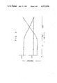
- FIG. 1 is a schematic view showing a crystal growing apparatus according to an embodiment of the present invention
- FIG. 2 is a graph showing the resistance between an electrode and a crystal raw material melt of the apparatus shown in FIG. 1 as a function of the distance therebetween;
- FIG. 3 is a graph showing how the resistance of the electrode changes with time.
- an electrode is arranged above a crystal raw material melt at a distance therefrom. Changes in the resistance of the atmosphere between the electrode and the melt are detected to thereby detect the surface level of the melt. The crystal pulling speed or supply of power for heating the melt is controlled in accordance with the detection result.
- the atmosphere around the crucible is generally Ar gas. According to an experiment conducted by the present inventor, it was found that a current passes through the atmosphere when an electrode is arranged over a melt at a distance therefrom and a voltage is applied between the electrode and the melt. It was also found that the atmospheric resistance increases exponentially in accordance with a descent in the surface level of the melt in the crucible. Although it is not clear whether these results are caused by ion conduction of a high-temperature gas or other mechanisms, the present invention utilizes these empirical results.
- FIG. 1 shows the schematic structure of a crystal growing apparatus according to an embodiment of the present invention.
- reference numeral 1 denotes a quartz crucible; 2, a silicon melt held in the crucible 1; 3, a heater arranged around the crucible 1; 4, a seed crystal shown in contact with the silicon melt 4; 5, a pulling shaft for pulling the seed crystal 4; 6, a crucible shaft rotated by a motor (not shown); and 7, a pulled silicon crystal.
- the basic structure of the apparatus remains the same as that of a conventional apparatus.
- an electrode 9 protected by a quartz tube 8 is arranged above the melt 2 held in the crucible 1.
- a distal end 9A of the electrode 9 consists of a p-type silicon carbide, and the proximal end is guided to the outside of the apparatus to be connected to the positive terminal of a dc power supply 11 through a lead wire 10 and a switch 21.
- the negative terminal of the dc power supply 11 is connected to one input terminal of a logarithmic operational amplifier 12.
- the other input terminal of the amplifier 12 is grounded.
- the crucible shaft 6 is also grounded by means of an electric brush or the like.
- a signal of a current passing in the atmosphere between the electrode 9 and the melt 2 appears at the output terminal of the amplifier 12.
- a reservoir 13 and a funnel 14 for supplying raw materials to the crucible 1 are arranged thereabove.
- the reservoir 13 has a reservoir controller 22 which includes a solenoid coil.
- the reservoir controller 22 controls the tilt angle of the reservoir 13 in accordance with an output signal from the amplifier 12 so as to control the amount of raw materials replenished to the crucible 1.
- Reference numeral 15 denotes a motor controller for regulating a pulling motor 16 which drives the pulling shaft 5
- 17 denotes a heater controller which controls power supply to the heater 3.
- An output signal from the amplifier 12 is selectively supplied to one or both of the controllers 15 and 17 so as to control the diameter of the crystal.
- the output terminal of the amplifier 12 is also connected to a level indicator 18.
- the rotational frequency of the pulling shaft 5 is optimally 6 to 10 rpm, and the pulling speed is preferably 2 mm/min.
- the crucible shaft 6 is rotated by a motor (not shown).
- the crucible shaft 6 is grounded as described above.
- the reservoir controller 22 for controlling the reservoir 13 is operated such that the polysilicon powder is continuously supplied from the reservoir 13 to the crucible 1 from a timing before the diameter of the pulled crystal stabilizes.
- the switch 21 of the dc power supply 11 is turned on to apply a dc bias to the electrode 9.
- the conduction current is amplified by the amplifier 12, and an output signal from the amplifier 12 is supplied to the level indicator 18 which indicates the surface level of the melt.
- the output signal from the amplifier 12 is also supplied to the reservoir controller 22.
- a decrease in the amount of the melt 2 upon the pulling operation of the seed crystal 4 is detected by the electrode 9. Then, the amount of the raw materials supplied to the crucible 1 is controlled in accordance with the relation given above. As a consequence, continuous and stable crystal growth can be performed. Furthermore, in the embodiment of the present invention, since continuous crystal growth can be performed, the length of the ingot can be made extremely long, resulting in a significant increase in the production yield. Since an additive such as an impurity can be supplied in a suitable amount to the reservoir 13 in advance, exponential change in the impurity concentration can be corrected and uniform crystals can be continuously manufactured.
- the diameter of the pulled crystal 7 is large, the surface of the melt 2 near the crucible 1 is inclined.
- the distal end 9A of the electrode 9 then opposes the inclined surface of the melt 2.
- This leads to a decrease in the distance X and hence to an increase in the conduction current.
- data on this is supplied to the motor controller 15 which supplies to the motor 16 a control signal to increase the pulling speed in accordance with the input data. Then, a decrease in the diameter is effected, so that the increase in the diameter is effectively suppressed. In this manner, the diameter of the pulled crystal is kept constant.
- Similar dimension control of a grown crystal can also be performed by controlling supply of power to the heater 3 by means of the heater controller 17.
- the distal end 9A of the electrode 9 consists of a p-type silicon carbide which is stable against use over a long period of time.
- FIG. 3 shows curves (indicated by a circle for the case wherein a p-type silicon carbide is used for the distal end 9A of the electrode 9, indicated by symbol x for the case wherein graphite is used, and indicated by a triangle for the case wherein an n-type silicon carbide is used) representing the changes in resistance as a function of time.
- the present invention is described with reference to a case wherein the distal end 9A of the electrode 9 comprises a p-type silicon carbide. However, if too high durability is not required, a p-type silicon carbide need not be used and other materials may be used.
- the surface level of a crystal raw material melt can be detected with ease and reliability, and dimension control of the pulled crystal can be performed in accordance with the detection result.
- Dimension control means diameter control in the Czochralski method, and thickness and width control in the ribbon pulling method.
- the apparatus of the present invention also facilitates continuous replenishment of the raw materials during crystal growth.
- the electrode since the electrode is arranged so as not to contact the melt, a surface level detector which has a simple structure and which has an excellent durability can be obtained.
- a surface level detector can be obtained which gives rise to only a small change in resistance over time.
Landscapes
- Chemical & Material Sciences (AREA)
- Engineering & Computer Science (AREA)
- Crystallography & Structural Chemistry (AREA)
- Materials Engineering (AREA)
- Metallurgy (AREA)
- Organic Chemistry (AREA)
- Crystals, And After-Treatments Of Crystals (AREA)
- Liquid Deposition Of Substances Of Which Semiconductor Devices Are Composed (AREA)
- Measurement Of Levels Of Liquids Or Fluent Solid Materials (AREA)
Abstract
Description
R=7.5×10.sup.5 exp (1.6×)
Claims (4)
Applications Claiming Priority (2)
| Application Number | Priority Date | Filing Date | Title |
|---|---|---|---|
| JP57143707A JPS5933554B2 (en) | 1982-08-19 | 1982-08-19 | crystal growth equipment |
| JP57-143707 | 1982-08-19 |
Publications (1)
| Publication Number | Publication Date |
|---|---|
| US4512954A true US4512954A (en) | 1985-04-23 |
Family
ID=15345098
Family Applications (1)
| Application Number | Title | Priority Date | Filing Date |
|---|---|---|---|
| US06/521,826 Expired - Lifetime US4512954A (en) | 1982-08-19 | 1983-08-10 | Crystal growing apparatus |
Country Status (2)
| Country | Link |
|---|---|
| US (1) | US4512954A (en) |
| JP (1) | JPS5933554B2 (en) |
Cited By (10)
| Publication number | Priority date | Publication date | Assignee | Title |
|---|---|---|---|---|
| EP0301998A1 (en) * | 1987-07-21 | 1989-02-01 | Shin-Etsu Handotai Company, Limited | Apparatus for adjusting initial position of melt surface |
| US4936947A (en) * | 1987-05-05 | 1990-06-26 | Mobil Solar Energy Corporation | System for controlling apparatus for growing tubular crystalline bodies |
| WO1991014027A1 (en) * | 1990-03-12 | 1991-09-19 | Mobil Solar Energy Corporation | System for controlling crystal growth apparatus and melt replenishment system therefor |
| US5124265A (en) * | 1990-10-15 | 1992-06-23 | Arizona Technology Development Corporation | Method and apparatus for crystallization process control |
| USRE34375E (en) * | 1987-05-05 | 1993-09-14 | Mobil Solar Energy Corporation | System for controlling apparatus for growing tubular crystalline bodies |
| US5357898A (en) * | 1991-10-22 | 1994-10-25 | Hitachi Metals, Ltd. | Method of producing single crystal and apparatus therefor |
| WO2000066817A1 (en) * | 1999-05-03 | 2000-11-09 | Evergreen Solar, Inc. | Melt depth control for semiconductor materials grown from a melt |
| US20040139910A1 (en) * | 2002-10-18 | 2004-07-22 | Sachs Emanuel Michael | Method and apparatus for crystal growth |
| US20050051080A1 (en) * | 2002-10-30 | 2005-03-10 | Wallace Richard Lee | Method and apparatus for growing multiple crystalline ribbons from a single crucible |
| US20110211995A1 (en) * | 2007-07-26 | 2011-09-01 | Calisolar, Inc. | Method and system for forming a silicon ingot using a low-grade silicon feedstock |
Families Citing this family (6)
| Publication number | Priority date | Publication date | Assignee | Title |
|---|---|---|---|---|
| JP2510541B2 (en) * | 1986-12-01 | 1996-06-26 | 株式会社日立製作所 | Magneto-resistive effect magnetic head for magnetic disk |
| JP2812949B2 (en) * | 1988-03-31 | 1998-10-22 | ソニー株式会社 | Magnetic disk device |
| JP2728487B2 (en) * | 1989-02-08 | 1998-03-18 | 株式会社日立製作所 | Recording / playback separation type magnetic head |
| SG71751A1 (en) | 1997-01-25 | 2000-04-18 | Tdk Corp | Thin film magnetic head and method of manufacturing the same |
| DE19983450B4 (en) | 1998-08-07 | 2006-07-20 | Nec Corp. | Semiconductor crystal pulling device and crystal pulling method |
| KR101027258B1 (en) | 2003-10-30 | 2011-06-14 | 주식회사 엘지실트론 | Single Crystal Ingot Growth Apparatus with Electrode Protection Device |
Citations (3)
| Publication number | Priority date | Publication date | Assignee | Title |
|---|---|---|---|---|
| US3980438A (en) * | 1975-08-28 | 1976-09-14 | Arthur D. Little, Inc. | Apparatus for forming semiconductor crystals of essentially uniform diameter |
| US4185076A (en) * | 1977-03-17 | 1980-01-22 | Mobil Tyco Solar Energy Corporation | Apparatus for controlled growth of silicon and germanium crystal ribbons |
| US4350557A (en) * | 1974-06-14 | 1982-09-21 | Ferrofluidics Corporation | Method for circumferential dimension measuring and control in crystal rod pulling |
-
1982
- 1982-08-19 JP JP57143707A patent/JPS5933554B2/en not_active Expired
-
1983
- 1983-08-10 US US06/521,826 patent/US4512954A/en not_active Expired - Lifetime
Patent Citations (3)
| Publication number | Priority date | Publication date | Assignee | Title |
|---|---|---|---|---|
| US4350557A (en) * | 1974-06-14 | 1982-09-21 | Ferrofluidics Corporation | Method for circumferential dimension measuring and control in crystal rod pulling |
| US3980438A (en) * | 1975-08-28 | 1976-09-14 | Arthur D. Little, Inc. | Apparatus for forming semiconductor crystals of essentially uniform diameter |
| US4185076A (en) * | 1977-03-17 | 1980-01-22 | Mobil Tyco Solar Energy Corporation | Apparatus for controlled growth of silicon and germanium crystal ribbons |
Cited By (23)
| Publication number | Priority date | Publication date | Assignee | Title |
|---|---|---|---|---|
| US4936947A (en) * | 1987-05-05 | 1990-06-26 | Mobil Solar Energy Corporation | System for controlling apparatus for growing tubular crystalline bodies |
| US5085728A (en) * | 1987-05-05 | 1992-02-04 | Mobil Solar Energy Corporation | System for controlling crystal growth apparatus and melt replenishment system therefor |
| USRE34375E (en) * | 1987-05-05 | 1993-09-14 | Mobil Solar Energy Corporation | System for controlling apparatus for growing tubular crystalline bodies |
| EP0301998A1 (en) * | 1987-07-21 | 1989-02-01 | Shin-Etsu Handotai Company, Limited | Apparatus for adjusting initial position of melt surface |
| US4915775A (en) * | 1987-07-21 | 1990-04-10 | Shin-Etsu Handotai Company, Ltd. | Apparatus for adjusting initial position of melt surface |
| WO1991014027A1 (en) * | 1990-03-12 | 1991-09-19 | Mobil Solar Energy Corporation | System for controlling crystal growth apparatus and melt replenishment system therefor |
| AU635125B2 (en) * | 1990-03-12 | 1993-03-11 | Schott Solar, Inc. | System for controlling crystal growth apparatus and melt replenishment system therefor |
| US5124265A (en) * | 1990-10-15 | 1992-06-23 | Arizona Technology Development Corporation | Method and apparatus for crystallization process control |
| US5357898A (en) * | 1991-10-22 | 1994-10-25 | Hitachi Metals, Ltd. | Method of producing single crystal and apparatus therefor |
| US6200383B1 (en) | 1999-05-03 | 2001-03-13 | Evergreen Solar, Inc. | Melt depth control for semiconductor materials grown from a melt |
| WO2000066817A1 (en) * | 1999-05-03 | 2000-11-09 | Evergreen Solar, Inc. | Melt depth control for semiconductor materials grown from a melt |
| US7708829B2 (en) | 2002-10-18 | 2010-05-04 | Evergreen Solar, Inc. | Method and apparatus for crystal growth |
| US20060249071A1 (en) * | 2002-10-18 | 2006-11-09 | Evergreen Solar, Inc. | Method and apparatus for crystal growth |
| US20080105193A1 (en) * | 2002-10-18 | 2008-05-08 | Evergreen Solar, Inc. | Method and Apparatus for Crystal Growth |
| US7407550B2 (en) | 2002-10-18 | 2008-08-05 | Evergreen Solar, Inc. | Method and apparatus for crystal growth |
| US20040139910A1 (en) * | 2002-10-18 | 2004-07-22 | Sachs Emanuel Michael | Method and apparatus for crystal growth |
| US7718003B2 (en) | 2002-10-18 | 2010-05-18 | Evergreen Solar, Inc. | Method and apparatus for crystal growth |
| US20050051080A1 (en) * | 2002-10-30 | 2005-03-10 | Wallace Richard Lee | Method and apparatus for growing multiple crystalline ribbons from a single crucible |
| US7022180B2 (en) | 2002-10-30 | 2006-04-04 | Evergreen Solar, Inc. | Method and apparatus for growing multiple crystalline ribbons from a single crucible |
| US20060191470A1 (en) * | 2002-10-30 | 2006-08-31 | Wallace Richard L Jr | Method and apparatus for growing multiple crystalline ribbons from a single crucible |
| US7507291B2 (en) | 2002-10-30 | 2009-03-24 | Evergreen Solar, Inc. | Method and apparatus for growing multiple crystalline ribbons from a single crucible |
| US20110211995A1 (en) * | 2007-07-26 | 2011-09-01 | Calisolar, Inc. | Method and system for forming a silicon ingot using a low-grade silicon feedstock |
| US8882912B2 (en) * | 2007-07-26 | 2014-11-11 | Silicor Materials Inc. | Method and system for forming a silicon ingot using a low-grade silicon feedstock |
Also Published As
| Publication number | Publication date |
|---|---|
| JPS5935088A (en) | 1984-02-25 |
| JPS5933554B2 (en) | 1984-08-16 |
Similar Documents
| Publication | Publication Date | Title |
|---|---|---|
| US4512954A (en) | Crystal growing apparatus | |
| US6241818B1 (en) | Method and system of controlling taper growth in a semiconductor crystal growth process | |
| US3980438A (en) | Apparatus for forming semiconductor crystals of essentially uniform diameter | |
| EP1068375B1 (en) | Open-loop method and system for controlling growth of semiconductor crystal | |
| JPH04149092A (en) | Method and device for controlling growth of cone part | |
| JPH07511B2 (en) | Method for manufacturing semiconductor silicon single crystal | |
| CN1329682A (en) | Method and apparatus for accurately pulling crystal | |
| US5096677A (en) | Single crystal pulling apparatus | |
| JPH08193975A (en) | Method and device for measuring and controlling oxygen concentration in fused silicon material | |
| JP2966322B2 (en) | Silicon single crystal ingot and manufacturing method thereof | |
| US4157373A (en) | Apparatus for the production of ribbon shaped crystals | |
| US3700412A (en) | Crystal pulling apparatus having means for maintaining liquid solid crystal interface at a constant temperature | |
| JP2008254946A (en) | Single crystal manufacturing apparatus, single crystal material, electronic component and single crystal manufacturing method | |
| JP2520925B2 (en) | Method for controlling oxygen concentration in silicon single crystal | |
| JPS5933553B2 (en) | crystal growth equipment | |
| US20050211157A1 (en) | Process control system for controlling a crystal-growing apparatus | |
| JP4815766B2 (en) | Silicon single crystal manufacturing apparatus and manufacturing method | |
| JP2003327494A (en) | Method for manufacturing silicon single crystal, program for operating silicon single crystal production, and apparatus for manufacturing silicon single crystal | |
| JP2520926B2 (en) | Method for controlling oxygen concentration in silicon single crystal | |
| JP2583811B2 (en) | Compound semiconductor single crystal growth method | |
| JPH0639353B2 (en) | Silicon single crystal pulling device | |
| JPS59121192A (en) | Preparation of single crystal of iii-v group compound semiconductor | |
| JP2582582B2 (en) | Silicon single crystal pulling equipment | |
| Batra et al. | Growth and characteristics of single crystals of lithium niobate | |
| JP2821962B2 (en) | Single crystal manufacturing equipment |
Legal Events
| Date | Code | Title | Description |
|---|---|---|---|
| AS | Assignment |
Owner name: TOKYO SHIBAURA DENKI KABUSHIKI KAISHA, 72 HORIKAWA Free format text: ASSIGNMENT OF ASSIGNORS INTEREST.;ASSIGNOR:MATSUI, TOSHIRO;REEL/FRAME:004162/0969 Effective date: 19830714 |
|
| STCF | Information on status: patent grant |
Free format text: PATENTED CASE |
|
| AS | Assignment |
Owner name: NEW ENERGY DEVELOPMENT ORGANIZATION, 1-1, 3-CHOME, Free format text: ASSIGNMENT OF ASSIGNORS INTEREST.;ASSIGNOR:KABUSHIKI KAISHA TOSHIBA;REEL/FRAME:004550/0308 Effective date: 19860506 Owner name: NEW ENERGY DEVELOPMENT ORGANIZATION, JAPAN Free format text: ASSIGNMENT OF ASSIGNORS INTEREST;ASSIGNOR:KABUSHIKI KAISHA TOSHIBA;REEL/FRAME:004550/0308 Effective date: 19860506 |
|
| FEPP | Fee payment procedure |
Free format text: PAYOR NUMBER ASSIGNED (ORIGINAL EVENT CODE: ASPN); ENTITY STATUS OF PATENT OWNER: LARGE ENTITY |
|
| FPAY | Fee payment |
Year of fee payment: 4 |
|
| FPAY | Fee payment |
Year of fee payment: 8 |
|
| FPAY | Fee payment |
Year of fee payment: 12 |