US4479174A - Efficiency increasing circuit for switching power supplies operating at low power levels - Google Patents
Efficiency increasing circuit for switching power supplies operating at low power levels Download PDFInfo
- Publication number
- US4479174A US4479174A US06/438,798 US43879882A US4479174A US 4479174 A US4479174 A US 4479174A US 43879882 A US43879882 A US 43879882A US 4479174 A US4479174 A US 4479174A
- Authority
- US
- United States
- Prior art keywords
- signal
- shift control
- generating
- control signal
- frequency shift
- Prior art date
- Legal status (The legal status is an assumption and is not a legal conclusion. Google has not performed a legal analysis and makes no representation as to the accuracy of the status listed.)
- Expired - Fee Related
Links
Images

Classifications
-
- H—ELECTRICITY
- H02—GENERATION; CONVERSION OR DISTRIBUTION OF ELECTRIC POWER
- H02M—APPARATUS FOR CONVERSION BETWEEN AC AND AC, BETWEEN AC AND DC, OR BETWEEN DC AND DC, AND FOR USE WITH MAINS OR SIMILAR POWER SUPPLY SYSTEMS; CONVERSION OF DC OR AC INPUT POWER INTO SURGE OUTPUT POWER; CONTROL OR REGULATION THEREOF
- H02M3/00—Conversion of DC power input into DC power output
- H02M3/22—Conversion of DC power input into DC power output with intermediate conversion into AC
- H02M3/24—Conversion of DC power input into DC power output with intermediate conversion into AC by static converters
- H02M3/28—Conversion of DC power input into DC power output with intermediate conversion into AC by static converters using discharge tubes with control electrode or semiconductor devices with control electrode to produce the intermediate AC
- H02M3/325—Conversion of DC power input into DC power output with intermediate conversion into AC by static converters using discharge tubes with control electrode or semiconductor devices with control electrode to produce the intermediate AC using devices of a triode or a transistor type requiring continuous application of a control signal
- H02M3/335—Conversion of DC power input into DC power output with intermediate conversion into AC by static converters using discharge tubes with control electrode or semiconductor devices with control electrode to produce the intermediate AC using devices of a triode or a transistor type requiring continuous application of a control signal using semiconductor devices only
- H02M3/33507—Conversion of DC power input into DC power output with intermediate conversion into AC by static converters using discharge tubes with control electrode or semiconductor devices with control electrode to produce the intermediate AC using devices of a triode or a transistor type requiring continuous application of a control signal using semiconductor devices only with automatic control of the output voltage or current, e.g. flyback converters
Definitions
- This invention relates to switching type power supplies and more particularly to a circuit adapted for use therein which increases the efficiency of the supply when it operates at or below some predetermined low power level.
- Switching type power supplies are used in the telephone art to provide a variety of voltages to a load.
- a switching type power supply in the form of a d-c to d-c converter may be used to provide ringing voltage and current (power) to the subscribers of a central office powered multichannel subscriber carrier system.
- the converter may have to provide a peak load power which is substantially higher than the relatively low load power it normally provides.
- Such converters are designed to have a relatively high efficiency and good stability when they provide such peak power. When such a converter provides the normal and relatively low load power, the efficiency and stability both decrease by substantial amounts.
- a circuit adapted for use in a switching converter of the type which utilizes pulse width modulations to generate, from a source of high frequency, signals whose width is dependent on the load connected to the supply.
- the circuit increases the efficiency and stability of the converter when it operates at or below some predetermined low power level.
- the circuit has a first means which includes a comparator which is responsive to a signal representative of converter output power level and a signal representative of the predetermined low power level for generating a frequency shift control which has a first amplitude when the output power level is above the reference and a second amplitude when that level is at least equal to if not less than the reference.
- the circuit also has a second means which responds to the frequency shift control signal and the high frequency signal for generating a signal which has a first and substantially constant waveform when the shift control signal has its first amplitude and a second waveform which is related to the predetermined waveform of the high frequency signal when the shift control signal has its second amplitude.
- the circuit has means to connect the efficiency increasing signal to the pulses in a manner such that the signal has no effect on the pulses when it has a constant waveform and eliminates pulses in a predetermined manner when it has the second waveform. The elimination of the pulses increases the efficiency of the supply at low power levels.
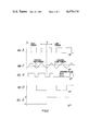
- FIG. 1 is a schematic diagram of a typical switching power converter which includes the circuit of the present invention.
- FIGS. 2(A) to (E) are waveforms of the voltages present at various designated locations in the circuit of FIG. 1.
- FIG. 1 there is shown a schematic circuit diagram of a d-c to d-c switching power supply 10 in accordance with the present invention.
- Supply 10 includes conventional switching converter 20 which uses the well-known pulse width modulation (p.w.m.) technique to drive power switching transistor Q1 to thereby provide from a d-c input voltage a regulated d-c output voltage across a load.
- the load is represented by the resistor R10.
- conventional converter 20 compares a d-c control voltage at analog comparator 22 to a sawtooth waveform whose frequency is typically 20 Khz or higher to thereby generate the drive signal in the form of pulses to transistor Q1.
- the sawtooth waveform is derived from a squarewave by the integrating circuit made up of resistor R8 and capacitor C2.
- the d-c control voltage is derived as a result of a comparison of a signal representative of the output voltage of the converter with a reference signal.
- the well-known circuitry used to generate the squarewave and provide the d-c control voltage at one input to comparator 22 has been omitted from FIG. 1.
- FIG. 2 there is shown in (A) thereof the high frequency squarewave from which the sawtooth waveform is derived.
- the sawtooth waveform is shown in (B) thereof.
- the squarewave appears in switching converter 20 at the junction designated by the letter “A” and after integration appears as the sawtooth waveform at the junction designated by the letter “B”.
- the sawtooth waveform is therefore connected to one input of comparator 22.
- the d-c control voltage which is applied to the other input of the comparator is also shown in FIG. 2(B).
- the amplitude of the d-c control voltage is dependent upon the load connected to supply 10 and decreases as supply 10 approaches essentially full load operation.
- the pulsed waveform is applied to the base of switching transistor Q1.
- Each pulse causes the transistor to conduct.
- the transistor conducts for a longer period of time for such operation as compared to its time of conduction for loads which are less than full loads.
- a transformer T1 is used to couple the voltage at the collector of the switching transistor to rectifying diode Dl and capacitor C3 to thereby provide a regulated d-c voltage at load resistor R10.
- the base of the transistor is connected to circuit common (COM).
- the values for the various circuit components used in conventional converter 20 are selected such that converter 20 has some desired efficiency and stability.
- the converter is designed for essentially full load operation.
- the circuit components are usually selected such that the converter has the desired efficiency and stability when it operates at essentially full load.
- the converter begins to operate at some lower power level which is less than the high power level associated with full load operation, its efficiency and stability suffer.
- the width of the drive pulses to transistor Q1 decreases. It is this decrease in pulse width which causes the drop in converter efficiency and stability at such low power levels.
- switching supply 10 includes input current or power level detector circuit 30 and frequency shifting circuit 40.
- circuits 30 and 40 function together in a manner so as to eliminate every other drive pulse to transistor Q1. The width of the remaining pulses must therefore increase in order that the transistor conduct for a period of time sufficient to supply the regulated voltage and meet the current requirements of the load. This increased drive pulse width allows switching supply 10 to operate with a more desirable efficiency and stability even at low power levels. Circuits 30 and 40 can be considered as functioning in combination as an efficiency and stability increasing circuit.
- FIGS. 2(A) to (C) show, as described above, the high frequency squarewave, the sawtooth waveform derived therefrom by the integrator and the drive pulses to transistor Q1.
- FIG. 2 shows, as described above, the high frequency squarewave, the sawtooth waveform derived therefrom by the integrator and the drive pulses to transistor Q1.
- Circuit 30 includes the series combination of resistors R2 and R3 which is connected between the relatively constant d-c input voltage to the supply and COM. The midpoint of the series combination is connected to the noninverting input of comparator 32. This connection provides a reference voltage to the noninverting input.
- a resistor R1 is connected in the manner illustrated between the input to supply 10 and the inverting input of comparator 32. The resistor R1 provides a voltage representative of the input current to supply 10 to the inverting input of the comparator. The input current varies with load and decreases as the load decreases. This connection therefore provides to the comparator a signal representative of the power level at which the supply operates.
- circuit 30 provides at the output of the comparator a signal which has a negative amplitude at high power levels and an essentially zero amplitude at low power levels.
- the signal at the output of the comparator is connected to frequency shift circuit 40 and will, therefore, be referred to hereinafter as the frequency shift control signal.
- circuit 30 has been shown as including a resistor R1 to provide from the input current a voltage representative of the power level at which the supply operates, it should be appreciated that this voltage may also be obtained by the use of suitably arranged circuitry which senses current at the load.
- Circuit 40 includes an input 46 which is connected to the output of comparator 32.
- a capacitor C1 connects input 46 to COM.
- the series combination of resistors R4 and R5 also connects input 46 to COM.
- the midpoint of this series combination designated by the capital letter “E"
- the frequency shift control signal is shown in FIG. 2(E) as it appears at midpoint E.
- the capacitor C1 provides smoothing for the signal at the output of comparator 32. The smoothing ensures that the signal has a relatively fast transition between its two amplitudes. Therefore, the signal at the output of the comparator 32 is essentially a scaled version and unsmoothed version of the signal shown in FIG. 2(E). Thus, the frequency shift control signal appears at the inverting input to comparator 44.
- the noninverting input of comparator 44 designated by the capital letter “D” is connected by a resistor R6 to the output of divide-by-2 circuit 42.
- the input of circuit 42 is connected to the junction A and therefore to the high frequency squarewave shown in FIG. 2(A).
- Circuit 42 divides the frequency of the squarewave by two such that a squarewave identical to that shown in FIG. 2(A) but at half the frequency shown therein appears at the noninverting input to comparator 44. This squarewave is shown in FIG. 2(D).
- Circuit 42 may be embodied by a flip-flop.
- the noninverting input of the comparator is also connected by a resistor R7 to COM.
- Circuit 40 operates in the following manner.
- the frequency shift control signal has the negative amplitude shown in FIG. 2(E) for the times between T0 and T1. This negative amplitude appears at the inverting input of comparator 44.
- the comparator is of the type which has an open collector at its output when its inverting input is held negative, the output of the comparator remains high independent of the squarewave appearing at its noninverting input. The high output of comparator 44 has no effect on the width modulated pulses appearing at junction C.
- the following example may provide further appreciation of the effect that the circuit of the present invention has on increasing the efficiency of a conventional switching converter when that converter operates at lower power levels.
- a converter designed to convert 20 V d-c to about 300 V d-c and deliver 14 watts of peak power the efficiency at that power level was over 80%.
- the efficiency decreased to about 63%.
- the circuit of the present invention was then added to the converter.
- the low power level at which that circuit began to operate and thereby improve converter efficiency was set at three (3) watts.
- a resistor of 1 ohm resistance was used for R1. With the circuit added the efficiency of the supply increased to about 75% at the three (3) watt level.
- circuit of the present invention has been described as increasing efficiency by eliminating every other drive pulse at low power levels, it should be appreciated that the circuit may be designed to eliminate pulses in some other predetermined manner.
- the use of a different circuit for divider 42 may allow for every third drive pulse to be eliminated. In any case, it is the elimination of the drive pulses in a predetermined manner for low power levels and the attendant increase in width of the remaining pulses which increases the efficiency of the converter at such power levels.
Landscapes
- Engineering & Computer Science (AREA)
- Power Engineering (AREA)
- Dc-Dc Converters (AREA)
Abstract
Description
Claims (8)
Priority Applications (1)
| Application Number | Priority Date | Filing Date | Title |
|---|---|---|---|
| US06/438,798 US4479174A (en) | 1982-11-03 | 1982-11-03 | Efficiency increasing circuit for switching power supplies operating at low power levels |
Applications Claiming Priority (1)
| Application Number | Priority Date | Filing Date | Title |
|---|---|---|---|
| US06/438,798 US4479174A (en) | 1982-11-03 | 1982-11-03 | Efficiency increasing circuit for switching power supplies operating at low power levels |
Publications (1)
| Publication Number | Publication Date |
|---|---|
| US4479174A true US4479174A (en) | 1984-10-23 |
Family
ID=23742061
Family Applications (1)
| Application Number | Title | Priority Date | Filing Date |
|---|---|---|---|
| US06/438,798 Expired - Fee Related US4479174A (en) | 1982-11-03 | 1982-11-03 | Efficiency increasing circuit for switching power supplies operating at low power levels |
Country Status (1)
| Country | Link |
|---|---|
| US (1) | US4479174A (en) |
Cited By (18)
| Publication number | Priority date | Publication date | Assignee | Title |
|---|---|---|---|---|
| US4772995A (en) * | 1987-01-08 | 1988-09-20 | Veeco Instruments Inc. | Switching supply with pulse width and rate modulation |
| US5949226A (en) * | 1995-04-10 | 1999-09-07 | Kabushiki Kaisha Toyoda Jidoshokki Seisakush | DC/DC converter with reduced power consumpton and improved efficiency |
| US5994885A (en) * | 1993-03-23 | 1999-11-30 | Linear Technology Corporation | Control circuit and method for maintaining high efficiency over broad current ranges in a switching regulator circuit |
| US6127815A (en) * | 1999-03-01 | 2000-10-03 | Linear Technology Corp. | Circuit and method for reducing quiescent current in a switching regulator |
| US6130528A (en) * | 1997-05-09 | 2000-10-10 | Kabushiki Kaisha Toyoda Jidoshokki Seisakusho | Switching regulator controlling system having a light load mode of operation based on a voltage feedback signal |
| US6195429B1 (en) * | 1997-04-23 | 2001-02-27 | Telefonaktiebolaget Lm Ericsson | Arrangement in a subscriber line interface circuit |
| US6307356B1 (en) | 1998-06-18 | 2001-10-23 | Linear Technology Corporation | Voltage mode feedback burst mode circuit |
| US6476589B2 (en) | 2001-04-06 | 2002-11-05 | Linear Technology Corporation | Circuits and methods for synchronizing non-constant frequency switching regulators with a phase locked loop |
| US6674274B2 (en) | 2001-02-08 | 2004-01-06 | Linear Technology Corporation | Multiple phase switching regulators with stage shedding |
| US20040095100A1 (en) * | 2002-11-19 | 2004-05-20 | Richard Thompson | Electrosurgical generator and method with voltage and frequency regulated high-voltage current mode power supply |
| US20050152164A1 (en) * | 1999-09-24 | 2005-07-14 | Balu Balakrishnan | Method and apparatus providing a multi-function terminal for a power supply controller |
| US7019507B1 (en) | 2003-11-26 | 2006-03-28 | Linear Technology Corporation | Methods and circuits for programmable current limit protection |
| US7030596B1 (en) | 2003-12-03 | 2006-04-18 | Linear Technology Corporation | Methods and circuits for programmable automatic burst mode control using average output current |
| US20070075790A1 (en) * | 2005-10-03 | 2007-04-05 | Linear Technology Corp. | Switching regulator duty cycle control in a fixed frequency operation |
| US8725218B2 (en) | 2011-03-25 | 2014-05-13 | R2 Semiconductor, Inc. | Multimode operation DC-DC converter |
| US9069365B2 (en) | 2012-02-18 | 2015-06-30 | R2 Semiconductor, Inc. | DC-DC converter enabling rapid output voltage changes |
| US9621036B2 (en) | 2014-01-09 | 2017-04-11 | Allegro Microsystems, Llc | Circuits and techniques for improving regulation in a regulator having more than one mode of operation |
| US10528072B2 (en) * | 2016-03-18 | 2020-01-07 | Ntn Corporation | Input voltage control device having three power lines |
Citations (3)
| Publication number | Priority date | Publication date | Assignee | Title |
|---|---|---|---|---|
| US3562668A (en) * | 1968-07-18 | 1971-02-09 | Gulf & Western Industries | Variable load controlled blocking oscillator power converter |
| US3978393A (en) * | 1975-04-21 | 1976-08-31 | Burroughs Corporation | High efficiency switching regulator |
| US4160945A (en) * | 1977-09-16 | 1979-07-10 | Wescom, Inc. | High efficiency switching regulator |
-
1982
- 1982-11-03 US US06/438,798 patent/US4479174A/en not_active Expired - Fee Related
Patent Citations (3)
| Publication number | Priority date | Publication date | Assignee | Title |
|---|---|---|---|---|
| US3562668A (en) * | 1968-07-18 | 1971-02-09 | Gulf & Western Industries | Variable load controlled blocking oscillator power converter |
| US3978393A (en) * | 1975-04-21 | 1976-08-31 | Burroughs Corporation | High efficiency switching regulator |
| US4160945A (en) * | 1977-09-16 | 1979-07-10 | Wescom, Inc. | High efficiency switching regulator |
Cited By (35)
| Publication number | Priority date | Publication date | Assignee | Title |
|---|---|---|---|---|
| US4772995A (en) * | 1987-01-08 | 1988-09-20 | Veeco Instruments Inc. | Switching supply with pulse width and rate modulation |
| US6304066B1 (en) | 1993-03-23 | 2001-10-16 | Linear Technology Corporation | Control circuit and method for maintaining high efficiency over broad current ranges in a switching regular circuit |
| US5994885A (en) * | 1993-03-23 | 1999-11-30 | Linear Technology Corporation | Control circuit and method for maintaining high efficiency over broad current ranges in a switching regulator circuit |
| US6580258B2 (en) | 1993-03-23 | 2003-06-17 | Linear Technology Corporation | Control circuit and method for maintaining high efficiency over broad current ranges in a switching regulator circuit |
| US5949226A (en) * | 1995-04-10 | 1999-09-07 | Kabushiki Kaisha Toyoda Jidoshokki Seisakush | DC/DC converter with reduced power consumpton and improved efficiency |
| US6157182A (en) * | 1995-04-10 | 2000-12-05 | Kabushiki Kaisha Toyoda | DC/DC converter with multiple operating modes |
| US6195429B1 (en) * | 1997-04-23 | 2001-02-27 | Telefonaktiebolaget Lm Ericsson | Arrangement in a subscriber line interface circuit |
| US6130528A (en) * | 1997-05-09 | 2000-10-10 | Kabushiki Kaisha Toyoda Jidoshokki Seisakusho | Switching regulator controlling system having a light load mode of operation based on a voltage feedback signal |
| US6307356B1 (en) | 1998-06-18 | 2001-10-23 | Linear Technology Corporation | Voltage mode feedback burst mode circuit |
| US6366066B1 (en) | 1999-03-01 | 2002-04-02 | Milton E. Wilcox | Circuit and method for reducing quiescent current in a switching regulator |
| US6127815A (en) * | 1999-03-01 | 2000-10-03 | Linear Technology Corp. | Circuit and method for reducing quiescent current in a switching regulator |
| US8482938B2 (en) | 1999-09-24 | 2013-07-09 | Power Integrations, Inc. | Method and apparatus providing a multi-function terminal for a power supply controller |
| US7876587B2 (en) | 1999-09-24 | 2011-01-25 | Power Integrations, Inc, | Method and apparatus providing a multi-function terminal for a power supply controller |
| US7253997B2 (en) | 1999-09-24 | 2007-08-07 | Power Integrations, Inc. | Method and apparatus providing a multi-function terminal for a power supply controller |
| US20090310389A1 (en) * | 1999-09-24 | 2009-12-17 | Power Integrations, Inc. | Method and apparatus providing a multi-function terminal for a power supply controller |
| US7596005B2 (en) | 1999-09-24 | 2009-09-29 | Power Integrations, Inc. | Method and apparatus providing a multi-function terminal for a power supply controller |
| US20050152164A1 (en) * | 1999-09-24 | 2005-07-14 | Balu Balakrishnan | Method and apparatus providing a multi-function terminal for a power supply controller |
| US20080186747A1 (en) * | 1999-09-24 | 2008-08-07 | Balu Balakrishnan | Method and apparatus providing a multi-function terminal for a power supply controller |
| US6674274B2 (en) | 2001-02-08 | 2004-01-06 | Linear Technology Corporation | Multiple phase switching regulators with stage shedding |
| US20050001602A1 (en) * | 2001-04-06 | 2005-01-06 | Linear Technology Corporation | Circuits and methods for synchronizing non-constant frequency switching regulators with a phase locked loop |
| US6774611B2 (en) | 2001-04-06 | 2004-08-10 | Linear Technology Corporation | Circuits and methods for synchronizing non-constant frequency switching regulators with a phase locked loop |
| US6476589B2 (en) | 2001-04-06 | 2002-11-05 | Linear Technology Corporation | Circuits and methods for synchronizing non-constant frequency switching regulators with a phase locked loop |
| US20020180413A1 (en) * | 2001-04-06 | 2002-12-05 | Linear Technology Corporation | Circuits and methods for synchronizing non-constant frequency switching regulators with a phase locked loop |
| US7019497B2 (en) | 2001-04-06 | 2006-03-28 | Linear Technology Corporation | Circuits and methods for synchronizing non-constant frequency switching regulators with a phase locked loop |
| US6939347B2 (en) | 2002-11-19 | 2005-09-06 | Conmed Corporation | Electrosurgical generator and method with voltage and frequency regulated high-voltage current mode power supply |
| US20040095100A1 (en) * | 2002-11-19 | 2004-05-20 | Richard Thompson | Electrosurgical generator and method with voltage and frequency regulated high-voltage current mode power supply |
| US7019507B1 (en) | 2003-11-26 | 2006-03-28 | Linear Technology Corporation | Methods and circuits for programmable current limit protection |
| US7030596B1 (en) | 2003-12-03 | 2006-04-18 | Linear Technology Corporation | Methods and circuits for programmable automatic burst mode control using average output current |
| US7388444B2 (en) | 2005-10-03 | 2008-06-17 | Linear Technology Corporation | Switching regulator duty cycle control in a fixed frequency operation |
| US20070075790A1 (en) * | 2005-10-03 | 2007-04-05 | Linear Technology Corp. | Switching regulator duty cycle control in a fixed frequency operation |
| US8725218B2 (en) | 2011-03-25 | 2014-05-13 | R2 Semiconductor, Inc. | Multimode operation DC-DC converter |
| US8843180B2 (en) | 2011-03-25 | 2014-09-23 | R2 Semiconductor, Inc. | Multimode operation DC-DC converter |
| US9069365B2 (en) | 2012-02-18 | 2015-06-30 | R2 Semiconductor, Inc. | DC-DC converter enabling rapid output voltage changes |
| US9621036B2 (en) | 2014-01-09 | 2017-04-11 | Allegro Microsystems, Llc | Circuits and techniques for improving regulation in a regulator having more than one mode of operation |
| US10528072B2 (en) * | 2016-03-18 | 2020-01-07 | Ntn Corporation | Input voltage control device having three power lines |
Similar Documents
| Publication | Publication Date | Title |
|---|---|---|
| US4479174A (en) | Efficiency increasing circuit for switching power supplies operating at low power levels | |
| US4980812A (en) | Uninterrupted power supply system having improved power factor correction circuit | |
| US4672518A (en) | Current mode control arrangement with load dependent ramp signal added to sensed current waveform | |
| US5003454A (en) | Power supply with improved power factor correction | |
| US5264780A (en) | On time control and gain circuit | |
| US4326245A (en) | Current foldback circuit for a DC power supply | |
| US5367247A (en) | Critically continuous boost converter | |
| US4412277A (en) | AC-DC Converter having an improved power factor | |
| US4302717A (en) | Power supply with increased dynamic range | |
| EP0582814B1 (en) | Dropout recovery circuit | |
| US4641233A (en) | AC to DC converter with voltage regulation | |
| US4493017A (en) | Single drive transformer with regenerative winding for p.w.m. supply having alternately conducting power devices | |
| US4220826A (en) | Ringing generator | |
| US5260996A (en) | Current limited electronic ringing generator | |
| US4293902A (en) | Transformerless fast current limiter with symetry correction for a switched-mode power supply | |
| US4309650A (en) | Average current controlled switching regulator utilizing digital control techniques | |
| US4628429A (en) | DC-DC converter with galvanically isolated feedback voltage regulation | |
| GB2195842A (en) | Controller for a resonant converter | |
| GB1468750A (en) | Regulation and stabilizing in a switching power supply | |
| US4631361A (en) | Programmable ring generator | |
| US7199562B2 (en) | Line frequency switching regulator | |
| EP0144344B1 (en) | Ringing signal generator | |
| US5070439A (en) | DC to DC converter apparatus employing push-pull oscillators | |
| US4788451A (en) | AC voltage stabilizer easily convertible into uninterruptible power supply (UPS) | |
| US5239453A (en) | DC to DC converter employing a free-running single stage blocking oscillator |
Legal Events
| Date | Code | Title | Description |
|---|---|---|---|
| AS | Assignment |
Owner name: RELIANCE ELECTRIC COMPANY, A CORP. OF DEL. Free format text: ASSIGNMENT OF ASSIGNORS INTEREST.;ASSIGNOR:CATES, ROBERT P.;REEL/FRAME:004064/0219 Effective date: 19821028 Owner name: RELIANCE ELECTRIC COMPANY, A CORP. OF DEL., STATEL Free format text: ASSIGNMENT OF ASSIGNORS INTEREST;ASSIGNOR:CATES, ROBERT P.;REEL/FRAME:004064/0219 Effective date: 19821028 |
|
| AS | Assignment |
Owner name: RELIANCE COMM/TEC CORPORATION, 8600 W. BRYN MAWR, Free format text: ASSIGNMENT OF ASSIGNORS INTEREST. EFFECTIVE DEC. 31, 1986.;ASSIGNOR:RELIANCE ELECTRIC COMPANY, A DE. CORP.;REEL/FRAME:004683/0435 Effective date: 19870310 |
|
| FPAY | Fee payment |
Year of fee payment: 4 |
|
| REMI | Maintenance fee reminder mailed | ||
| LAPS | Lapse for failure to pay maintenance fees | ||
| FP | Lapsed due to failure to pay maintenance fee |
Effective date: 19921025 |
|
| STCH | Information on status: patent discontinuation |
Free format text: PATENT EXPIRED DUE TO NONPAYMENT OF MAINTENANCE FEES UNDER 37 CFR 1.362 |