US4456879A - Method and apparatus for determining the doping profile in epitaxial layers of semiconductors - Google Patents
Method and apparatus for determining the doping profile in epitaxial layers of semiconductors Download PDFInfo
- Publication number
- US4456879A US4456879A US06/298,581 US29858181A US4456879A US 4456879 A US4456879 A US 4456879A US 29858181 A US29858181 A US 29858181A US 4456879 A US4456879 A US 4456879A
- Authority
- US
- United States
- Prior art keywords
- layer
- epitaxial layer
- variations
- laser beam
- photocurrent
- Prior art date
- Legal status (The legal status is an assumption and is not a legal conclusion. Google has not performed a legal analysis and makes no representation as to the accuracy of the status listed.)
- Expired - Lifetime
Links
Images


Classifications
-
- G—PHYSICS
- G01—MEASURING; TESTING
- G01R—MEASURING ELECTRIC VARIABLES; MEASURING MAGNETIC VARIABLES
- G01R31/00—Arrangements for testing electric properties; Arrangements for locating electric faults; Arrangements for electrical testing characterised by what is being tested not provided for elsewhere
- G01R31/26—Testing of individual semiconductor devices
- G01R31/265—Contactless testing
- G01R31/2656—Contactless testing using non-ionising electromagnetic radiation, e.g. optical radiation
-
- Y—GENERAL TAGGING OF NEW TECHNOLOGICAL DEVELOPMENTS; GENERAL TAGGING OF CROSS-SECTIONAL TECHNOLOGIES SPANNING OVER SEVERAL SECTIONS OF THE IPC; TECHNICAL SUBJECTS COVERED BY FORMER USPC CROSS-REFERENCE ART COLLECTIONS [XRACs] AND DIGESTS
- Y10—TECHNICAL SUBJECTS COVERED BY FORMER USPC
- Y10S—TECHNICAL SUBJECTS COVERED BY FORMER USPC CROSS-REFERENCE ART COLLECTIONS [XRACs] AND DIGESTS
- Y10S148/00—Metal treatment
- Y10S148/093—Laser beam treatment in general
Definitions
- This invention relates to the determination of the doping profile in epitaxial layers of semiconductors.
- an epitaxial layer is approximately 50-100 ⁇ m thick and it provides the basis for the active part of the device. Accordingly, the epitaxial layer is doped during growth from the gas phase in a very precise and well-defined way in order to obtain the required doping profile across the epitaxial layer. For example, for an NPN transistor, located near the substrate, one has an intrinsic layer as a collector field region followed by a P-type base region and an N-type emitter region. It is very important to control and monitor the doping profile for such a transistor very accurately.
- Monitoring the doping profile can be done, for example, by sacrificing one wafer from each batch that is being processed and grinding a beveled edge through the epitaxial layer of such a wafer.
- the conductivity is measured across the epitaxial layer with a 2-point probe technique by which 10-100 points are used for the conductivity measurements.
- a 2-point probe technique by which 10-100 points are used for the conductivity measurements.
- the present invention provides for an apparatus and method for determining the doping profile in epitaxial layers of semiconductors by modifying a direct current flowing through the epitaxial layer with photocurrents generated by a focused laser beam modulated at high frequencies in the order of 20 MHz. A change in the flow of d.c. current effected by the laser generated photocurrent is monitored to determine the resistivity for each of a plurality of points to which the laser beam is directed.
- FIG. 1 is a schematic of the prior art technique using a 2-point probe to determine a doping profile
- FIG. 2 is a schematic of an apparatus of one embodiment of the present invention.
- FIG. 3 is a schematic of a model of a portion of an epitaxial layer for illustrating the principle of the present invention
- FIG. 4 is a schematic of a modification of the epitaxial layer for practicing the invention.
- FIG. 5 is a schematic of another modification of the epitaxial layer for practicing the invention.
- FIG. 6 is a typical plot of resistivity plotted against the depth illustrating the invention.
- FIG. 1 illustrating a device on which a 2-point probe is used to generate a doping profile as described, for example, in the above-identified Modern Microelectronics text.
- a semiconductor body such as a wafer 10 includes a substrate 12 and an epitaxial layer 14.
- a bevel 16 is provided in the surface to increase the resolution of the doping profile. The bevel is achieved by a technique known as angle lapping which is costly.
- a pair of probes 18 and 20 are positioned to contact the surface portion 16 of the epitaxial layer 14. D.C. measurements with apparatus, not shown, are made by applying a d.c. voltage across the probes 18 and 20. The probes are repositioned at various locations along the surface 16 with measurements being made at each location.
- the resistivity (or, if desired, conductivity) is determined by calculation and plotted in a suitable manner to generate what is known as a doping profile.
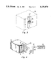
- a wafer 20 having a substrate 22 and an epitaxial layer 24 is provided with a metallic layer 26 on an exposed surface of the epitaxial layer 24 and a metallic conductive layer 28 on the bottom surface of the substrate 22.
- the wafer is cut to form a flat surface 30.
- monocrystalline layers such as silicon layers with their planar surfaces oriented parallel to the (110) plane the wafer 20 may be simply broken to provide the surface 30.
- an angle lap of the wafer 20 may be provided similar to that as shown in FIG. 1.
- the embodiment being described comprises a wafer formed of silicon. Nevertheless, it should be understood that the invention may be used to determine the doping profile of wafers formed of germanium, gallium arsenide or other semiconductor materials.
- a direct current voltage source 32 such as the battery having a terminal voltage V 0 , is connected to the metallic layer 26 and to the substrate conductor layer 28 through a resistor 34 at the common ground 36.
- a laser 38 suitably a red He-Ne laser at a wavelength of 0.6328 ⁇ m, provides a beam 40, passed through an optical modulator 42 and thence through a pair of lenses 44 and 46, such as a beam expander 47, and thence to a lens 48, such as as a microscope objective.
- These optical components are arranged to generate a very fine beam 50 of modulated laser light that is oriented to impinge on a surface portion 52 (in general, portion P) of the surface 30.
- Apparatus (not shown) provides a means to move either the wafer 20 or the light beam apparatus to cause the beam 50 to be directed to any one of a series of points located along the surface 30.
- the modulator 42 provides a modulated beam of at least 1 MHz, but preferably at 20 MHz as will be explained hereinafter.
- the size or diameter of the focused beam 50 is typically 1 ⁇ m or less.
- the photocurrent generated by the laser beam is monitored according to the invention by a capacitor 54 coupling the voltage across resistor 34 to a detector 56 whose output is coupled to a meter 58.
- Detector 56 is a suitable detector such as a filter, a phase sensitive detection amplifier or a heterodyning circuit, as known in the art for detecting a high frequency variation in a d.c. signal. Detector 56 thus provides a current signal from which the conductivity or resistivity of the material at the particular point 52 to which the laser beam 50 was directed can be determined.
- the meter 58 will indicate the current (j 1 ) or, if desired, the doping concentration (N L ) as will be explained.
- the resistivity (or conductivity) is calculated, as well known in the art, from the (1) carrier mobility, (2) doping concentration and (3) electron charge.
- any other device such as a computer plotter 59 (or printer) can be coupled to the detector 56 to provide a plot or print out of the resistivity (or conductivity) directly.
- the beam position is provided to the plotter (from beam-positioning means not shown) so that the plotter 59 can relate the resistivity in ohm-cm with the laser scanned surface of the depth in microns.
- FIG. 6 for a plot of a typical doping profile using data that is generated by the apparatus of FIG. 2.
- a doping profile curve 60 is generated by the individual points PI . . . PN to which the beam 50 was in sequence directed.
- the resistivity in ohm-cm versus the depth along surface distance is shown plotted in microns.
- the beam 50 when directed to the surface 30 at each point P, generates a photocurrent caused by a decrease of the resistance in the layer 24 due to the photogeneration of the electrons and holes at each point P.
- the effect of the photocarriers generated at each point P depends on the dark resistance and the doping at the location P. In particular, the effect of the photogeneration will be large if the resistance is high, and the doping concentration is low. The converse is true if the resistance is low and the doping concentration is high. Accordingly, the change of the current I due to the laser irradiation by beam 50 is used as a measure for the doping at each location P exposed to the laser beam spot. The change in the current I is often called the photocurrent.
- spacial resolution of this testing procedure is not as fine as the focus of the laser beam 50 because the cloud of electrons and holes spreads and broadens by the diffusion process. If one were to use laser light that was unmodulated and of constant intensity, the spreading effect would be characterized by the minority diffusion length
- the wavelength of the laser 38 is chosen such that the light penetration into the silicon material of the epitaxial layer 24 is large enough to have a reasonable effect on the photocurrent. Moreover, the wavelength sould not be so large as to sacrifice focus and spacial resolution.
- the preferred form of laser according to these guidelines for silicon is a He-Ne laser with a wavelength of 0.6328 ⁇ m.
- the penetration of the beam 50 from such a laser into silicon is about 3 ⁇ m, which value it will be noticed, is equal to the solution of equation (2) described above.
- the filament 62 in reality is embedded in a real sample as represented by the dashed lines 64 of about 100 times the width and 100 times the depth.
- the model calculation of equation (3) is reduced by a factor of 10 4 , resulting in the value of the ratio j 1 /J>5 ⁇ 10 -7 .
- Such a current ratio value is large enough to be detected by state-of-the-art electronic filtering techniques as illustrated by detector 56 in FIG. 2.
- the high frequency photocurrent j 1 is inversely proportional to the square of the doping concentration at the light spot position.
- FIG. 4 illustrating a modification of the wafer arrangement for determining the doping profile according to the invention.
- a wafer 70 having an epitaxial layer 72, is provided with a pair of metallic striped coatings 74 and 76 serving as the metallic contacts.
- a voltage source 78 is connected to terminal 74 and to ground.
- the other contact 76 is connected to a resistor 80 and a capacitor 82.
- the capacitor 82 is connected to the measuring apparatus 84 such as detector 56 and meter 58 illustrated in FIG. 2.
- the pair of striped contacts 74 and 76 are applied to a cleaved, cross-sectioned or beveled surface 73 of the epitaxial layer 72.
- the laser beam 50 is directed to the surface portion 82 between the conductors 74 and 76 in sequence at various points. At each position of the beam 50 a measurement is made of the photocurrent variations. It will be noticed that the current flow generated by the arrangement of FIG. 4 is parallel to the plane of the epitaxial layer 72 as along dotted line 85. Nevertheless, a photoconductor component of the current due to the modulated laser beam 50 is measured.
- FIG. 5 illustrating another arrangement for the measurement of a doping profile.
- a wafer 86 has an epitaxial layer 88 and a highly conductive substrate 90.
- a metallic contact 92 is applied to the extremity of a negative-beveled surface 94.
- the laser beam 50 is applied to the surface 94 in sequence at different locations to develop the doping profile.
- the current flow will follow generally the contoured lines 96.
- the sensitivity of the profile measurements is increased by constraining the current 96 to the surface 94 in the negatively beveled sample.
Landscapes
- Physics & Mathematics (AREA)
- Health & Medical Sciences (AREA)
- Electromagnetism (AREA)
- Toxicology (AREA)
- General Physics & Mathematics (AREA)
- Testing Or Measuring Of Semiconductors Or The Like (AREA)
Abstract
Description
L=√Dτ (1)
L.sub.eff =√D/2πf (2)
Claims (18)
Priority Applications (1)
| Application Number | Priority Date | Filing Date | Title |
|---|---|---|---|
| US06/298,581 US4456879A (en) | 1981-09-02 | 1981-09-02 | Method and apparatus for determining the doping profile in epitaxial layers of semiconductors |
Applications Claiming Priority (1)
| Application Number | Priority Date | Filing Date | Title |
|---|---|---|---|
| US06/298,581 US4456879A (en) | 1981-09-02 | 1981-09-02 | Method and apparatus for determining the doping profile in epitaxial layers of semiconductors |
Publications (1)
| Publication Number | Publication Date |
|---|---|
| US4456879A true US4456879A (en) | 1984-06-26 |
Family
ID=23151141
Family Applications (1)
| Application Number | Title | Priority Date | Filing Date |
|---|---|---|---|
| US06/298,581 Expired - Lifetime US4456879A (en) | 1981-09-02 | 1981-09-02 | Method and apparatus for determining the doping profile in epitaxial layers of semiconductors |
Country Status (1)
| Country | Link |
|---|---|
| US (1) | US4456879A (en) |
Cited By (20)
| Publication number | Priority date | Publication date | Assignee | Title |
|---|---|---|---|---|
| US4564808A (en) * | 1983-03-11 | 1986-01-14 | The United States Of America As Represented By The United States Department Of Energy | Direct determination of quantum efficiency of semiconducting films |
| US4581576A (en) * | 1984-04-23 | 1986-04-08 | Hewlett-Packard Company | Nondestructive method for profiling imperfection levels in high resistivity semiconductor wafers |
| USH111H (en) | 1985-11-21 | 1986-08-05 | The United States Of America As Represented By The Secretary Of The Navy | Gallium arsenide material and process evaluation by means of pulsed photoconductance in test devices |
| US4777146A (en) * | 1987-02-24 | 1988-10-11 | American Telephone And Telegraph Company, At&T Bell Laboratories | Fabrication process involving semi-insulating material |
| US4891582A (en) * | 1986-09-24 | 1990-01-02 | Technion Research & Development Foundation | Optical apparatus and method for photocarrier diffusion length measurement |
| US5082792A (en) * | 1990-08-15 | 1992-01-21 | Lsi Logic Corporation | Forming a physical structure on an integrated circuit device and determining its size by measurement of resistance |
| US5171399A (en) * | 1990-08-15 | 1992-12-15 | The United States Of America As Represented By The United States Department Of Energy | Reflection mass spectrometry technique for monitoring and controlling composition during molecular beam epitaxy |
| US5200693A (en) * | 1991-02-26 | 1993-04-06 | Cornell Research Foundation, Inc. | Method for determining characteristics of pn semiconductor structures |
| US5217907A (en) * | 1992-01-28 | 1993-06-08 | National Semiconductor Corporation | Array spreading resistance probe (ASRP) method for profile extraction from semiconductor chips of cellular construction |
| US5442297A (en) * | 1994-06-30 | 1995-08-15 | International Business Machines Corporation | Contactless sheet resistance measurement method and apparatus |
| US5504016A (en) * | 1991-03-29 | 1996-04-02 | National Semiconductor Corporation | Method of manufacturing semiconductor device structures utilizing predictive dopant-dopant interactions |
| US5519334A (en) * | 1994-09-29 | 1996-05-21 | Advanced Micro Devices, Inc. | System and method for measuring charge traps within a dielectric layer formed on a semiconductor wafer |
| US6005400A (en) * | 1997-08-22 | 1999-12-21 | Lockheed Martin Energy Research Corporation | High resolution three-dimensional doping profiler |
| KR20000073640A (en) * | 1999-05-13 | 2000-12-05 | 황인길 | Apparatus and for measuring doping profile |
| US6218848B1 (en) * | 1998-02-25 | 2001-04-17 | Micron Technology, Inc. | Semiconductor probe card having resistance measuring circuitry and method of fabrication |
| US6297653B1 (en) | 1999-06-28 | 2001-10-02 | Micron Technology, Inc. | Interconnect and carrier with resistivity measuring contacts for testing semiconductor components |
| US6664797B1 (en) * | 1999-10-29 | 2003-12-16 | Advanced Micro Devices, Inc. | Method for profiling semiconductor device junctions using a voltage contrast scanning electron microscope |
| US7512499B1 (en) | 2006-12-20 | 2009-03-31 | National Semiconductor Corporation | System and method for determining substrate doping density in metal oxide semiconductor devices |
| CN102856225A (en) * | 2012-08-16 | 2013-01-02 | 顺德中山大学太阳能研究院 | Detection method of selective doping region property |
| CN110118725A (en) * | 2018-02-07 | 2019-08-13 | 清华大学 | Photoelectric current scanning system |
Citations (4)
| Publication number | Priority date | Publication date | Assignee | Title |
|---|---|---|---|---|
| US3518545A (en) * | 1968-04-25 | 1970-06-30 | Bell Telephone Labor Inc | Methods and apparatus for measuring semiconductor doping profiles by determining second harmonic content |
| US3745454A (en) * | 1971-12-03 | 1973-07-10 | Motorola Inc | Method and means for measuring carrier lifetime in epitaxial films |
| US4180784A (en) * | 1977-09-19 | 1979-12-25 | The Boeing Company | Frequency modulated electrical discharge laser |
| US4205265A (en) * | 1978-08-21 | 1980-05-27 | Rca Corporation | Laser beam apparatus and method for analyzing solar cells |
-
1981
- 1981-09-02 US US06/298,581 patent/US4456879A/en not_active Expired - Lifetime
Patent Citations (4)
| Publication number | Priority date | Publication date | Assignee | Title |
|---|---|---|---|---|
| US3518545A (en) * | 1968-04-25 | 1970-06-30 | Bell Telephone Labor Inc | Methods and apparatus for measuring semiconductor doping profiles by determining second harmonic content |
| US3745454A (en) * | 1971-12-03 | 1973-07-10 | Motorola Inc | Method and means for measuring carrier lifetime in epitaxial films |
| US4180784A (en) * | 1977-09-19 | 1979-12-25 | The Boeing Company | Frequency modulated electrical discharge laser |
| US4205265A (en) * | 1978-08-21 | 1980-05-27 | Rca Corporation | Laser beam apparatus and method for analyzing solar cells |
Non-Patent Citations (2)
| Title |
|---|
| Modern Microelectronics, by Max Fogiel, Research and Education Association, New York, N.Y., 1972, pp. 376 379; 412 413. * |
| Modern Microelectronics, by Max Fogiel, Research and Education Association, New York, N.Y., 1972, pp. 376-379; 412-413. |
Cited By (22)
| Publication number | Priority date | Publication date | Assignee | Title |
|---|---|---|---|---|
| US4564808A (en) * | 1983-03-11 | 1986-01-14 | The United States Of America As Represented By The United States Department Of Energy | Direct determination of quantum efficiency of semiconducting films |
| US4581576A (en) * | 1984-04-23 | 1986-04-08 | Hewlett-Packard Company | Nondestructive method for profiling imperfection levels in high resistivity semiconductor wafers |
| USH111H (en) | 1985-11-21 | 1986-08-05 | The United States Of America As Represented By The Secretary Of The Navy | Gallium arsenide material and process evaluation by means of pulsed photoconductance in test devices |
| US4891582A (en) * | 1986-09-24 | 1990-01-02 | Technion Research & Development Foundation | Optical apparatus and method for photocarrier diffusion length measurement |
| US4777146A (en) * | 1987-02-24 | 1988-10-11 | American Telephone And Telegraph Company, At&T Bell Laboratories | Fabrication process involving semi-insulating material |
| US5082792A (en) * | 1990-08-15 | 1992-01-21 | Lsi Logic Corporation | Forming a physical structure on an integrated circuit device and determining its size by measurement of resistance |
| US5171399A (en) * | 1990-08-15 | 1992-12-15 | The United States Of America As Represented By The United States Department Of Energy | Reflection mass spectrometry technique for monitoring and controlling composition during molecular beam epitaxy |
| US5200693A (en) * | 1991-02-26 | 1993-04-06 | Cornell Research Foundation, Inc. | Method for determining characteristics of pn semiconductor structures |
| US5504016A (en) * | 1991-03-29 | 1996-04-02 | National Semiconductor Corporation | Method of manufacturing semiconductor device structures utilizing predictive dopant-dopant interactions |
| US5217907A (en) * | 1992-01-28 | 1993-06-08 | National Semiconductor Corporation | Array spreading resistance probe (ASRP) method for profile extraction from semiconductor chips of cellular construction |
| US5442297A (en) * | 1994-06-30 | 1995-08-15 | International Business Machines Corporation | Contactless sheet resistance measurement method and apparatus |
| US5519334A (en) * | 1994-09-29 | 1996-05-21 | Advanced Micro Devices, Inc. | System and method for measuring charge traps within a dielectric layer formed on a semiconductor wafer |
| US6005400A (en) * | 1997-08-22 | 1999-12-21 | Lockheed Martin Energy Research Corporation | High resolution three-dimensional doping profiler |
| US6218848B1 (en) * | 1998-02-25 | 2001-04-17 | Micron Technology, Inc. | Semiconductor probe card having resistance measuring circuitry and method of fabrication |
| KR20000073640A (en) * | 1999-05-13 | 2000-12-05 | 황인길 | Apparatus and for measuring doping profile |
| US6297653B1 (en) | 1999-06-28 | 2001-10-02 | Micron Technology, Inc. | Interconnect and carrier with resistivity measuring contacts for testing semiconductor components |
| US6664797B1 (en) * | 1999-10-29 | 2003-12-16 | Advanced Micro Devices, Inc. | Method for profiling semiconductor device junctions using a voltage contrast scanning electron microscope |
| US7512499B1 (en) | 2006-12-20 | 2009-03-31 | National Semiconductor Corporation | System and method for determining substrate doping density in metal oxide semiconductor devices |
| CN102856225A (en) * | 2012-08-16 | 2013-01-02 | 顺德中山大学太阳能研究院 | Detection method of selective doping region property |
| CN102856225B (en) * | 2012-08-16 | 2015-09-09 | 顺德中山大学太阳能研究院 | A kind of detection method of selective doping region characteristic |
| CN110118725A (en) * | 2018-02-07 | 2019-08-13 | 清华大学 | Photoelectric current scanning system |
| US11190132B2 (en) * | 2018-02-07 | 2021-11-30 | Tsinghua University | Photocurrent scanning system |
Similar Documents
| Publication | Publication Date | Title |
|---|---|---|
| US4456879A (en) | Method and apparatus for determining the doping profile in epitaxial layers of semiconductors | |
| US4287473A (en) | Nondestructive method for detecting defects in photodetector and solar cell devices | |
| US4758786A (en) | Method of analyzing semiconductor systems | |
| US4949034A (en) | Method for contactless evaluation of characteristics of semiconductor wafers and devices | |
| US4473795A (en) | System for resist defect measurement | |
| US4563642A (en) | Apparatus for nondestructively measuring characteristics of a semiconductor wafer with a junction | |
| US9880200B2 (en) | Method and apparatus for non-contact measurement of forward voltage, saturation current density, ideality factor and I-V curves in P-N junctions | |
| US4839588A (en) | Method for the examination of electrically active impurities of semiconductor materials or structures and measuring arrangement for carrying out the method | |
| US9110127B2 (en) | Apparatus and method for electrical characterization by selecting and adjusting the light for a target depth of a semiconductor | |
| US4464627A (en) | Device for measuring semiconductor characteristics | |
| US4168212A (en) | Determining semiconductor characteristic | |
| US7642772B1 (en) | Non-contact method and apparatus for measurement of leakage current of p-n junctions in IC product wafers | |
| CN110940860A (en) | Optical method for measuring resistivity of silicon wafer in non-contact mode | |
| US4028207A (en) | Measuring arrangements | |
| CA1225435A (en) | System for measuring carrier lifetime of semiconductor wafers | |
| US9921261B2 (en) | Method and apparatus for non-contact measurement of sheet resistance and shunt resistance of p-n junctions | |
| MacDonald et al. | Direct measurement of the depletion layer width variation vs applied bias for ap‐n junction | |
| US7414409B1 (en) | Non-contact method and apparatus for measurement of leakage current of p-n junctions in IC product wafers | |
| Bajaj et al. | Remote contact LBIC imaging of defects in semiconductors | |
| US4494069A (en) | Optical scanning method of testing material defects | |
| JPH0697252A (en) | Method and apparatus for decision of thickness of polysilicon/silicon interface oxide film | |
| US3039056A (en) | Testing of semiconductors | |
| JPH07240450A (en) | Method for measuring carrier life | |
| US4238686A (en) | Method of analyzing localized nonuniformities in luminescing materials | |
| JPH113923A (en) | Method for detecting metal contaminants in submicron silicon surface layer of semiconductor |
Legal Events
| Date | Code | Title | Description |
|---|---|---|---|
| AS | Assignment |
Owner name: RCA CORPORATION, A CORP. OF DE. Free format text: ASSIGNMENT OF ASSIGNORS INTEREST.;ASSIGNOR:KLEINKNECHT, HANS P.;REEL/FRAME:003917/0094 Effective date: 19810828 Owner name: RCA CORPORATION, A CORP. OF DE., STATELESS Free format text: ASSIGNMENT OF ASSIGNORS INTEREST;ASSIGNOR:KLEINKNECHT, HANS P.;REEL/FRAME:003917/0094 Effective date: 19810828 |
|
| STCF | Information on status: patent grant |
Free format text: PATENTED CASE |
|
| FPAY | Fee payment |
Year of fee payment: 4 |
|
| FPAY | Fee payment |
Year of fee payment: 8 |
|
| FEPP | Fee payment procedure |
Free format text: PAYOR NUMBER ASSIGNED (ORIGINAL EVENT CODE: ASPN); ENTITY STATUS OF PATENT OWNER: LARGE ENTITY |
|
| FPAY | Fee payment |
Year of fee payment: 12 |
|
| AS | Assignment |
Owner name: INTERSIL CORPORATION, FLORIDA Free format text: ASSIGNMENT OF ASSIGNORS INTEREST;ASSIGNOR:HARRIS SEMICONDUCTOR PATENTS, INC.;REEL/FRAME:010247/0161 Effective date: 19990813 |
|
| AS | Assignment |
Owner name: CREDIT SUISSE FIRST BOSTON, AS COLLATERAL AGENT, N Free format text: SECURITY INTEREST;ASSIGNOR:INTERSIL CORPORATION;REEL/FRAME:010351/0410 Effective date: 19990813 |