US4430564A - Image conversion apparatus with gas discharge switching - Google Patents
Image conversion apparatus with gas discharge switching Download PDFInfo
- Publication number
- US4430564A US4430564A US06/271,620 US27162081A US4430564A US 4430564 A US4430564 A US 4430564A US 27162081 A US27162081 A US 27162081A US 4430564 A US4430564 A US 4430564A
- Authority
- US
- United States
- Prior art keywords
- gas
- array
- capacitor
- electrodes
- insulating layer
- Prior art date
- Legal status (The legal status is an assumption and is not a legal conclusion. Google has not performed a legal analysis and makes no representation as to the accuracy of the status listed.)
- Expired - Fee Related
Links
Images


Classifications
-
- H—ELECTRICITY
- H01—ELECTRIC ELEMENTS
- H01J—ELECTRIC DISCHARGE TUBES OR DISCHARGE LAMPS
- H01J17/00—Gas-filled discharge tubes with solid cathode
- H01J17/38—Cold-cathode tubes
Definitions
- This invention relates to image conversion apparatus; more particularly it relates to an image conversion apparatus of high resolution having a line array of light responsive circuits each of which responds to light from a discrete point along a line of a relatively moving original document to be scanned; and specifically to an image conversion apparatus wherein each of said circuits comprises the capacitance defined by an elemental area of a photoconductive insulating layer connected in series with a capacitor across a voltage source with a gas space arranged, when ignited, to short said capacitor whereby the resulting charging current to the capacitance of the associated photoconductive insulating layer, proportional to the quantity of light incident thereon, is measured.
- Apparatus for horizontally scanning strips of an original image point by point for conversion to electrical signals using a linear array of charge coupled devices (CCD's) consisting of a shift register arrangement with 1728 devices are known.
- CCD's charge coupled devices
- a resolution of 8 dots per millimeter can be obtained.
- the length of such an array is on the order of 25 mm, to scan the DIN A 4 size page requires optical reduction of the image and, as optics require significant space, the advantage due to the small size of the CCD's is not realized.
- the construction of a CCD array differs from the construction of known apparatus for recording the serial dot video signals generated at the output of the CCD array.
- the different constructions require different manufacturing techniques which preclude cost efficiencies.
- an array of discrete light responsive circuits comprising the capacitance of a photoconductive insulator in series with a capacitor which is shunted by a switch. All of the circuits are arranged in parallel and connected across a voltage source. According to the dot resolution desired the ground plate of the capacitor and the insulating layer between the plates of the capacitor are preforated to define gas gaps each of which is in communication with an associated gas chamber bounded by the ground plate of the capacitor and a discrete electrode spaced from the ground plate.
- both the capacitance of the photoconductive insulating layer and the capacitor With source voltage applied and light incident on the circuits, both the capacitance of the photoconductive insulating layer and the capacitor will be charged to levels determined by the intensity and period of application of the incident light.
- a switch associated with a discrete light responsive circuit When a switch associated with a discrete light responsive circuit is closed and its capacitor is discharged, the level of charge stored in the capacitance of the photoconductive insulator will rise to the voltage of the source, with the magnitude of the change representing the light incident on the discrete circuit.
- a current will flow over the switch open interval in an amount proportional to light, reducing the charge stored in the capacitance of the photoconductive insulator and increasing the charge in the capacitor until the switch is again closed to read out its associated circuit.
- the light responsive circuits of the array are scanned or read out in turn by applying read pulses to three switching lines. More particularly, the first, fourth, seventh, etc. circuits are connected to one switching line, the second, fifth, eighth, etc., to a second switching line, and the third, sixth, ninth, etc. to a third switching line. Three phase displaced trains of voltage pulses of sufficient magnitude are applied to the switching lines to discharge the gas chambers and effect switch closures from left to right in turn.
- channels connecting gas chambers in the array are provided to carry ions from a discharged gas chamber into the next following gas chamber.
- ions are introduced into the first gas chamber of the array of circuits to lower its breakdown potential whereby discharge will occur upon application of a read voltage pulse of a magnitude normally insufficient to effect discharge.
- the discharge in the first gas chamber will prime the second gas chamber with discharge therein priming the third, etc., whereby the image exposed array is serially scanned.
- An object of the invention is in the provision of a 1:1 image converter.
- Another object of the invention is in the provision of a 1:1 image converter capable of high resolution without the necessity for optical reduction of the image to be converted.
- a further object of the invention is in the provision of a visual to electronic image converter capable of high speed line-scanning.
- a further object of the invention is to provide an image converter having parts common to a recorder to enable cost efficient manufacture of both units.
- FIG. 1 is a schematic diagram of an image converter comprising an array of light responsive circuits in accordance with the invention
- FIG. 2 is cross sectional view showing the physical construction of a portion of an image converter schematically shown in FIG. 1.
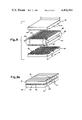
- FIG. 3 is an exploded perspective view showing details of the construction shown in FIG. 2;
- FIG. 4 is a pulse timing diagram for reading out or scanning each circuit in the array from left to right in turn;
- FIG. 5 is a cross-sectional view taken along lines 5--5 of FIG. 2 showing light sources for illuminating an original and fiber optics for conveying light reflected from the original to the circuits of the array;
- FIG. 6 is an elevational view of the image converter apparatus
- FIG. 7 is a schematic circuit diagram of a reproduction array known to the art.
- FIG. 8 is an elevational view showing the physical construction, in accordance with the invention, of a portion of the reproduction array schematically shown in FIG. 7;
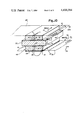
- FIGS. 9 and 9a are views showing the method of making fiber optic and/or recording pin support sub-assemblies of the image converting and reproduction arrays.
- FIG. 10 is a perspective view of an image converting and reproduction array on a common support particularly suited to a copy machine application.
- FIG. 1 a light to electrical image converter comprising an array of light responsive circuits generally designated by reference numerals 1, 2, 3, 4, 5, 6 - - - n.
- Each of the light responsive circuits comprises the capacitance C ph and parallel resistance R ph of a discrete area of a layer of a photoconductive insulator in series with a capacitor C, which is shunted by a switch S.
- the circuits 1-n are connected in parallel across a d-c source voltage V via a common series resistance R.
- the switches S 1 -S n associated with light responsive circuit 1-n are briefly closed, in turn, once each line scan. The closure of a switch S shorts its associated capacitor C with the result that it discharges and its associated capacitance C ph charges to the source voltage V over the interval of closure of switch S.
- FIGS. 2 and 3 there is shown the construction of an image converter according to a preferred embodiment of the invention comprising an array of parallel fiber optic rods 7 of discrete cross sectional area fixed, in a manner hereinafter described, in a fabricated glass assembly 8.
- a transparent conductive coating 9 on which a layer 11 of photoconductive insulating material is deposited.
- Coating 9 constitutes the upper plate of the parallel capacitances C ph .
- coatings of conductive material constituting floating electrodes 12 are deposited over discrete areas coextensive with the cross sectional area of the fiber optic rods 7.
- the floating electrodes 12 associated with each circuit represent the lower plate of capacitor C ph , the upper plate of capacitor C and the left terminal of switch S.
- a conductive coating 13 representing the lower plate of capacitor C or ground electrode is separated from the floating electrodes 12 by an insulating layer 14 of a material such as SiO 2 . Opposite the center of each of the floating electrodes 12, the insulating layer 14 and the ground electrode 13 are etched through to the floating electrode 12, creating gas gaps 15 which, in conducting state, assume the function of switches S.
- the conductance of gas gaps 15 is controlled by gas discharges initiated in a gas chambers 16 which are controlled by application of negative read voltage pulses ⁇ 1 , ⁇ 2 , ⁇ 3 to electrodes 17 coated on a lower glass support plate 18.
- Electrodes 17 are positioned in alignment with floating electrodes 12 and are spaced from ground electrode 13 by the thickness of a perforated conductive plate 21 whose perforations 22 define the gas chambers 16 which are bounded vertically by electrodes 17 and ground electrode 13 and bounded laterally by the walls 23 of the perforations 22 in the plate 21.
- channels 24 are etched through the walls 23 between perforations 22 of the plate 21 and connect one gas chamber 16 to its adjacent gas chambers 16.
- the perforated plate 21 is insulated from support plate 18 by insulating spacers 25.
- the relative dimensions are greatly enlarged for purpose of clarity of explanation.
- the gas chambers 16 are on the order of 50-100 microns square and 30-50 microns high.
- a gas discharge will occur between an electrode 17 as cathode and a grounded electrode 13 or perforated plate 21 as anode.
- the penetration of the discharge from cathode 17 to the floating electrode 12 is very small and the gas gap 15 is virtually decoupled from all processes in the gas chamber 16, unless there is a difference in potential between the floating and ground electrodes 12 and 13.
- a stray field from the edges of electrode 13 is effective into the gas gap 15 towards floating electrode 12.
- This causes a transport of charge carriers from the gas discharge in gas chamber 16 towards the electrode 12 until the potential difference between the electrodes 12 and 13 is equalized.
- the charging current produces a voltage drop proportional to the intensity of light incident on the discrete area of the photoconductive insulating layer 11 during a scan interval which is coupled to signal output terminal T via a coupling capacity C K . Since the measured signal is proportional to the quantity of incident light, a continuous halftone image reproduction is possible.
- the time required to equalize the difference in potential between the floating and grounds electrodes 12 and 13 is a few hundred nano seconds so that the duration of the read pulses ⁇ 1 , ⁇ 2 , ⁇ 3 applied to electrodes 17 to read or scan the circuits 1-n can be less than one microsecond.
- the statistical potential deviation remaining at the floating electrode 12 after the gas discharge versus the electrode 13 at ground potential is less than 10 mV. As the useful signals are roughly 10 volts, signal-to-noise ratios of approx. 1000:1 (60 dB) can be realized.
- a 1:1 image converter in accordance with the invention will be as wide as the width of an original document to be scanned.
- the image converter will be 21 centimeters wide and, to realize a resolution of 10 dots per millimeter, will have 2100 discrete light responsive circuits 1-n arranged at 0.1 millimeter intervals.
- three lines 26, 27 and 28 are employed as shown in FIG. 1 to carry three phase read pulses ⁇ 1 , ⁇ 2 , and ⁇ 3 .
- the sequence of negative pulses ⁇ 1 , ⁇ 2 and ⁇ 3 each, for example, of one microsecond duration as shown in FIG. 4, will read out the circuits 1-n at a one megahertz rate. More particularly, line 26 is connected to the first, fourth, seventh, etc. electrodes 17, line 27 is connected to the 2nd, 5th, 8th, etc. electrodes 17 and line 28 is connected to the 3rd, 6th, 9th etc. electrodes 17.
- the magnitude of the negative pulses ⁇ 1 , ⁇ 2 , ⁇ 3 on lines 26, 27, and 28 is normally less than the breakdown potential of the gas chambers 16 and thus will not cause a discharge unless the gas chambers 16 are primed.
- ions from a previously ignited gas chamber 16 are introduced into the next to be ignited gas chamber 16.
- the gas chamber 16 of the first circuit 1 is primed to initiate a line scan, by ions from a starting gas chamber 31 (FIGS.
- the negative magnitude of the pulse ⁇ s is chosen to exceed the breakdown potential of starting gas chamber 31 whereby a discharge from electrodes 17 to 13 thereof occurs without delay, in that electrons are made available at the cathode 17 by field emission.
- the discharge thus triggered is completed after a few hundred nanoseconds.
- Sufficient ions from this starting gas chamber 31 are diffused through the channel 24 between the starting gas chamber 31 and the first gas chamber 16 of the circuit array, lowering its threshold of breakdown.
- the starting voltage pulse ⁇ s is discontinued and a read voltage pulse ⁇ 1 , of lower magnitude than pulse ⁇ s , is applied at time t 1 to line 26. Due to the diffusion of charge via channel 24 between the start gas chamber 31 and the gas chamber 16 of the first circuit in the array, the voltage pulse ⁇ 1 on line 26 is sufficient to initiate a discharge in the first gas chamber 16. It is, however, insufficient to initiate breakdown in the gas chambers 16 associated with sensor circuits 4, 7, 10 etc., which not having being primed, continue to have a breakdown potential higher than the magnitude of the pulses ⁇ 1 applied to line 26.
- the discharge in the gas chamber 16 associated with the first circuit 1 brings its floating electrode 12 to ground potential, and at the same time ions diffuse through the channel 24 between the gas chamber 16 of the first circuit in the array to the gas chamber 16 of the second circuit 2 in the array.
- the voltage pulse ⁇ 1 is no longer applied to line 26.
- the information stored in the primed second circuit 2 in the array is thus read out and the third circuit 3 is primed to be read, etc. with the pulses ⁇ 1 - ⁇ 3 on lines 26, 27 and 28 causing gas discharges to shift from the gas chamber 16 of one sensor to another from left to right in turn.
- the gas chamber 16 of fourth circuit 4 in the array is primed and read upon receipt of a pulse ⁇ 1 at time t 4 on line 26, via which circuit 1 was read out earlier.
- circuit 1 is not again read, as any ions still present in its gas chamber 16, after its extinction at time t 1 , is neutralized at the walls 23 thereof. Due to the very small size of the gas chambers 16, this process of neutralization is completed very quickly before the application of the next pulse on a given line, thus enabling the step-by-step continuation of the gas discharges with only three phase pulses ⁇ 1 , ⁇ 2 and ⁇ 3 to be realized.
- a switch S can be closed only if an immediately previous switch S has been closed.
- a voltage pulse ⁇ s is again applied on start line 32 to initiate another scan of the array.
- capacitors C ph are recharged consecutively to the level of the source voltage V from the decreased levels obtained during open switch intervals, thus producing individual signals at the output terminal, T, proportional to the intensity of light incident on discrete areas of the photoconductive insulating layer 11 during a line scan time. Accordingly, a line image is resolved or split into n discrete points with line feed being accomplished by moving the original being scanned.
- the scanning array with an integrated space saving lighting system which makes a distortion free 1:1 exposure possible to the edges of a document 33.
- the upper glass plate 8 which is fabricated as will hereinafter appear with reference to FIG. 9, supports the fiber optic glass rods 7 opposite elemental areas of the photoconductive insulating layer 11 to be read out.
- the chambers 35 and 36 extend to either side of the line array of fiber optic rods 7 and the light therefrom is directed toward the original 33 and is reflected therefrom through the fiber optic rods 7 and transparent electrode 9 to thereby expose the underlying discrete elemental area of the photoconductive insulating layer 11. Further, as shown in FIG. 5 a light absorbing coating 38 is applied to the upper glass plate 8 except where the fiber optic rods 7 penetrate the surface of the glass assembly 8. Due to the close spacing of the light sources 35 and 36 (3 mm approx.) the intensity of the exposure of the original 33 is relatively high.
- the fabricated glass assembly 8 supporting the fiber optic rods 7 is adjusted over and glued to the glass support plate 18 by means of an epoxy resin 41, after which gas chambers 16 in the assembly are evacuated through a pump nipple 42, and filled with gas, such as neon +0.1% argon to approximately 1 atmosphere of pressure after which the pump nipple 42 is melted off.
- gas such as neon +0.1% argon to approximately 1 atmosphere of pressure after which the pump nipple 42 is melted off.
- the leads applied to the glass assembly 8 and support plate 18 in the form of thin films, as described with reference to FIGS. 1, 2, and 3 run below the epoxy resin layer 41 and form external terminals collectively designated by reference 43.
- FIG. 7 there is shown a schematic of a reproduction unit, generally designated by reference numeral 44 for recording signals generated by the image converter.
- the reproduction unit 44 comprises an array of metal recording pins 45 corresponding in number to the circuits 1-n of the image converter.
- the pins 45 are selected in turn, after a negative start pulse ⁇ s is applied, by application of three phase negative pulses ⁇ 1 , ⁇ 2 , ⁇ 3 to cathodes 46 to effect gas discharges to a common anode 47 in a manner similar to that described with reference to the scanning array of FIGS. 1 and 2.
- the operation of such a reproduction array 44 is more particularly described in the IEEE Transactions on Electron Devices, Vol. Ed.-21 No.
- the recording pins 45 are spaced a short distance from a dielectric paper copy sheet 48 on a conductive plate electrode 51 to which the serially generated dot video signals from the output terminal T (FIG. 1) of the image converter to be recorded are applied.
- the recording pins 45 are maintained during discharge at a voltage higher than the cathode 46 and, if the potential between a recording pin 45 and electrode 51 exceeds the breakdown potential of the air gap between recording pin and recording paper 48, discharge occurs with the result the dielectric paper 48 is charged in an amount related to the magnitude of the dot video signal.
- the charge pattern can later be developed as known in electrophotography.
- FIG. 8 there is shown a portion of the physical construction of a reproduction unit, including a recording pin 45, in accordance with the invention.
- the cathodes 46 comprise films of discrete area deposited on a glass support plate 53.
- the perforations in the plate 55 which constitutes the anode 47 in FIG.
- each gas chamber 57 communicates with adjacent chambers 57 by means of interconnecting channels 58 whereby each chamber 57 may be primed in turn by discharge in an earlier chamber 57 in the array as described in the image scanning array of FIG. 2.
- a starting gas chamber 59 (FIG. 7) to the left of the recording pin array starts a scan when a pulse ⁇ s is applied to its cathode 46.
- the construction of the reproduction unit 44 as shown has elements identical in construction and geometry to elements of the image converter of FIG. 2. More particularly, the glass support plate 53, cathodes 46, gas chambers 57, perforated plate 55 with channels 58 to diffuse ions, and the insulating spacers 56 of FIG. 8, are identical to the glass support plate 18, cathodes 17, gas chambers 16, perforated plate 21, channels 24 and insulating spacers 25 of FIG. 2, thus offering manufacturing efficiencies.
- the recording pins 45 are supported in a fabricated glass assembly 60 which is substantially similar to the glass assembly 8 supporting the fiber optic rods 7. Both therefore lend themselves to fabrication by the same production technique as shown in FIGS. 9 and 9a to which reference is now made.
- One surface each of the plates 61-64 is provided, using photolithographic techniques, with grooves 65, the depth of which is smaller than the radius of strands 66 (fiber optic or metal wire strands) used, and the width of which roughly matches the diameter of the strands 66.
- the center distance of the grooves 65 corresponds to the specified dot resolution, i.e. 10 grooves/mm, for instance.
- the middle plates 62 and 63 are fixed so that their grooves 65 face outwardly.
- the radius of the fixtures 67 and 68 is greater than the smallest permissible bending radius of the strands 66 used.
- the grooves 65 are filled with epoxy resin 69 and wound with a continuous strand 66 so that a length of the strand 66 is placed in each groove 65.
- the grooves 65 of plates 61 and 64 are also filled with epoxy resin and pressed groove side toward the strand wound plates 62 and 63 so that the wound strand 66 fits in the grooves 65 of plates 61 and 64.
- the plates 61 and 64 are provided with parallel, transverse slots 71 approx. 1 mm wide 0.5 mm deep, and approx. 3 mm apart.
- FIG. 9a One pair, 61-62, is shown in FIG. 9a from which strips 72 are sawed at right angles to the strands 66 in the transverse slots 65. After grinding and polishing the sawed surfaces, more than 100 fabricated glass strip assemblies are obtained as shown in FIG. 9a whose cut strands, either fiber optic rod 7 or metal pin 45, are supported at the proper spacing by the grooves 65. Each strip assembly thus constitutes either the fiber optic rod assembly 8 of FIG. 2 or the metal pin assembly 60 of FIG. 8.
- the structures of the image converter not common to the reproduction array are produced by well known thin-film techniques and photolithographic methods.
- FIG. 10 there is shown a back to back arrangement of an image converting unit and a reproduction unit 44 carried on the upper and lower surfaces of a common support plate 73. Signals at the output terminal T of the converter are connected over line 74 to electrode 51 of the reproduction unit 44.
- an original document 33 to be scanned or read will be moved, message side down, across the line of the array of fiber optic rods 7 and a copy document 75 on which the message on the original document is to be reproduced will be moved, message side up, across the line of the array of recording pins 45.
- the original and copy documents 33 and 75 are moved in the same direction indicated by arrows 76, the original document 33 will, as viewed in FIG. 10, be read or scanned in a left to right direction 77, and the copy document 75 written on in a right to left direction 78 in order that a right reading copy of the message 79 on document 33 will be recorded.
- the original and copy documents 33 and 75 are moved in opposite directions the original and copy documents will both be read and written in the same left to right direction to produce a right reading copy document.
- the direction of the gas discharges can be controlled from n-1 as well as from 1-n simply by providing auxiliary starting gas chambers 35 at both ends of the arrays.
- the auxiliary starting gas chamber on the right side is ignited for each start and the pulse sequence ⁇ 1 , ⁇ 2 , ⁇ 3 reversed to ⁇ 3 , ⁇ 2 , ⁇ 1 .
Landscapes
- Facsimile Heads (AREA)
Abstract
Description
Claims (9)
Priority Applications (1)
| Application Number | Priority Date | Filing Date | Title |
|---|---|---|---|
| US06/271,620 US4430564A (en) | 1981-06-08 | 1981-06-08 | Image conversion apparatus with gas discharge switching |
Applications Claiming Priority (1)
| Application Number | Priority Date | Filing Date | Title |
|---|---|---|---|
| US06/271,620 US4430564A (en) | 1981-06-08 | 1981-06-08 | Image conversion apparatus with gas discharge switching |
Publications (1)
| Publication Number | Publication Date |
|---|---|
| US4430564A true US4430564A (en) | 1984-02-07 |
Family
ID=23036342
Family Applications (1)
| Application Number | Title | Priority Date | Filing Date |
|---|---|---|---|
| US06/271,620 Expired - Fee Related US4430564A (en) | 1981-06-08 | 1981-06-08 | Image conversion apparatus with gas discharge switching |
Country Status (1)
| Country | Link |
|---|---|
| US (1) | US4430564A (en) |
Cited By (6)
| Publication number | Priority date | Publication date | Assignee | Title |
|---|---|---|---|---|
| US4531062A (en) * | 1981-11-20 | 1985-07-23 | Triumph-Adler Aktiengesellschaft Fur Buro- Und Informationstechnik | Document scanning apparatus |
| US4551622A (en) * | 1982-04-02 | 1985-11-05 | Triumph-Adler Aktiengesellschaft Fur Buro- Und Informationstechnik | Document scanning apparatus with photosensor and gas discharge readout |
| US4583126A (en) * | 1982-11-18 | 1986-04-15 | Xerox Corporation | Raster input/output scanner |
| US4672221A (en) * | 1982-11-01 | 1987-06-09 | Tokyo Shibaura Denki Kabushiki Kaisha | Photoelectric conversion element with light shielding conductive layer |
| US4783651A (en) * | 1983-10-03 | 1988-11-08 | Ta Triumph-Alder Aktiengesellschaft | Linear D.C. gas discharge displays and addressing techniques therefor |
| US6784069B1 (en) * | 2003-08-29 | 2004-08-31 | Micron Technology, Inc. | Permeable capacitor electrode |
Citations (2)
| Publication number | Priority date | Publication date | Assignee | Title |
|---|---|---|---|---|
| US2925530A (en) | 1956-11-28 | 1960-02-16 | Digital Tech Inc | Luminous display device |
| US4079422A (en) | 1976-10-12 | 1978-03-14 | Eastman Kodak Company | Charge injection device readout |
-
1981
- 1981-06-08 US US06/271,620 patent/US4430564A/en not_active Expired - Fee Related
Patent Citations (2)
| Publication number | Priority date | Publication date | Assignee | Title |
|---|---|---|---|---|
| US2925530A (en) | 1956-11-28 | 1960-02-16 | Digital Tech Inc | Luminous display device |
| US4079422A (en) | 1976-10-12 | 1978-03-14 | Eastman Kodak Company | Charge injection device readout |
Cited By (9)
| Publication number | Priority date | Publication date | Assignee | Title |
|---|---|---|---|---|
| US4531062A (en) * | 1981-11-20 | 1985-07-23 | Triumph-Adler Aktiengesellschaft Fur Buro- Und Informationstechnik | Document scanning apparatus |
| US4551622A (en) * | 1982-04-02 | 1985-11-05 | Triumph-Adler Aktiengesellschaft Fur Buro- Und Informationstechnik | Document scanning apparatus with photosensor and gas discharge readout |
| US4672221A (en) * | 1982-11-01 | 1987-06-09 | Tokyo Shibaura Denki Kabushiki Kaisha | Photoelectric conversion element with light shielding conductive layer |
| US4583126A (en) * | 1982-11-18 | 1986-04-15 | Xerox Corporation | Raster input/output scanner |
| US4783651A (en) * | 1983-10-03 | 1988-11-08 | Ta Triumph-Alder Aktiengesellschaft | Linear D.C. gas discharge displays and addressing techniques therefor |
| US6784069B1 (en) * | 2003-08-29 | 2004-08-31 | Micron Technology, Inc. | Permeable capacitor electrode |
| US20060192239A1 (en) * | 2003-08-29 | 2006-08-31 | Patraw Robert D | Permeable capacitor electrode |
| US7179706B2 (en) | 2003-08-29 | 2007-02-20 | Micron Technology, Inc. | Permeable capacitor electrode |
| US7329917B2 (en) | 2003-08-29 | 2008-02-12 | Micron Technology, Inc. | Permeable capacitor electrode |
Similar Documents
| Publication | Publication Date | Title |
|---|---|---|
| KR940004689A (en) | Bi-channel electrode structure of address structure using ionizable gas medium and its operation method | |
| CA2210402A1 (en) | Flat panel detector and image sensor | |
| EP0806689A2 (en) | Methods and apparatus for a multi-electrode micromechanical optical modulator | |
| EP0030292A2 (en) | Charge transfer device incorporating Laplacian thresholding with a time delay and integration imaging array | |
| US3158430A (en) | Transducing apparatus | |
| US4103204A (en) | Flat display device with beam guide | |
| US3611019A (en) | Gas panel apparatus and method | |
| US2247684A (en) | Photoelectric sorting apparatus | |
| US4837631A (en) | Electronic still camera tube | |
| GB1153673A (en) | Improvements in or relating to Electrical Discharge Display Devices | |
| US3890500A (en) | Apparatus for sensing radiation and providing electrical readout | |
| US3870257A (en) | Electrostatic recording using discharge space potential | |
| JPS5999649A (en) | Flat type image reproducing device | |
| US5500572A (en) | High resolution image source | |
| US3840740A (en) | Imaging device having solid-state target | |
| US4607269A (en) | Electrostatic print head | |
| DE1614911A1 (en) | Display and storage device | |
| US3633064A (en) | Signal converting system using barrier grid-type storage tube | |
| US3750190A (en) | Electrostatic recording device utilizing the electric potential in a discharge space | |
| JPH0229269B2 (en) | ||
| US3676732A (en) | Photo-electronic imaging apparatus | |
| US4392194A (en) | Circuit arrangement for controlling a large number of printing electrodes for non-mechanical printing | |
| JPS5518151A (en) | Input device of photo electric conversion information | |
| US4783651A (en) | Linear D.C. gas discharge displays and addressing techniques therefor | |
| US3445589A (en) | Electrical scanning apparatus |
Legal Events
| Date | Code | Title | Description |
|---|---|---|---|
| AS | Assignment |
Owner name: TRIUMPH-ADLER A.G.FUR BURO-UND INFORMATIONSTECHNIK Free format text: ASSIGNMENT OF ASSIGNORS INTEREST.;ASSIGNOR:FISCHER, DIETER;REEL/FRAME:003894/0052 Effective date: 19810504 |
|
| AS | Assignment |
Owner name: RESIDENCE INN COMPANY,THE, A TENNESSEE GENERAL PAR Free format text: ASSIGNMENT OF ASSIGNORS INTEREST.;ASSIGNOR:BROCK RESIDENCE INNS,INC.;REEL/FRAME:004367/0089 Effective date: 19850110 |
|
| MAFP | Maintenance fee payment |
Free format text: PAYMENT OF MAINTENANCE FEE, 4TH YEAR, PL 96-517 (ORIGINAL EVENT CODE: M170); ENTITY STATUS OF PATENT OWNER: LARGE ENTITY Year of fee payment: 4 |
|
| FEPP | Fee payment procedure |
Free format text: PAYOR NUMBER ASSIGNED (ORIGINAL EVENT CODE: ASPN); ENTITY STATUS OF PATENT OWNER: LARGE ENTITY |
|
| MAFP | Maintenance fee payment |
Free format text: PAYMENT OF MAINTENANCE FEE, 8TH YEAR, PL 96-517 (ORIGINAL EVENT CODE: M171); ENTITY STATUS OF PATENT OWNER: LARGE ENTITY Year of fee payment: 8 |
|
| FEPP | Fee payment procedure |
Free format text: MAINTENANCE FEE REMINDER MAILED (ORIGINAL EVENT CODE: REM.); ENTITY STATUS OF PATENT OWNER: LARGE ENTITY |
|
| LAPS | Lapse for failure to pay maintenance fees | ||
| FP | Lapsed due to failure to pay maintenance fee |
Effective date: 19960207 |
|
| STCH | Information on status: patent discontinuation |
Free format text: PATENT EXPIRED DUE TO NONPAYMENT OF MAINTENANCE FEES UNDER 37 CFR 1.362 |