US4400813A - Crenelated-ridge waveguide laser - Google Patents
Crenelated-ridge waveguide laser Download PDFInfo
- Publication number
- US4400813A US4400813A US06/285,253 US28525381A US4400813A US 4400813 A US4400813 A US 4400813A US 28525381 A US28525381 A US 28525381A US 4400813 A US4400813 A US 4400813A
- Authority
- US
- United States
- Prior art keywords
- ridge
- notched
- semiconductor laser
- layer
- regions
- Prior art date
- Legal status (The legal status is an assumption and is not a legal conclusion. Google has not performed a legal analysis and makes no representation as to the accuracy of the status listed.)
- Expired - Lifetime
Links
- 230000000737 periodic effect Effects 0.000 claims abstract description 14
- 239000004065 semiconductor Substances 0.000 claims description 17
- GPXJNWSHGFTCBW-UHFFFAOYSA-N Indium phosphide Chemical compound [In]#P GPXJNWSHGFTCBW-UHFFFAOYSA-N 0.000 claims description 6
- 239000000758 substrate Substances 0.000 claims description 4
- 239000000463 material Substances 0.000 claims description 3
- GYHNNYVSQQEPJS-UHFFFAOYSA-N Gallium Chemical compound [Ga] GYHNNYVSQQEPJS-UHFFFAOYSA-N 0.000 claims 1
- OAICVXFJPJFONN-UHFFFAOYSA-N Phosphorus Chemical compound [P] OAICVXFJPJFONN-UHFFFAOYSA-N 0.000 claims 1
- 229910052785 arsenic Inorganic materials 0.000 claims 1
- RQNWIZPPADIBDY-UHFFFAOYSA-N arsenic atom Chemical compound [As] RQNWIZPPADIBDY-UHFFFAOYSA-N 0.000 claims 1
- 229910052733 gallium Inorganic materials 0.000 claims 1
- 229910052738 indium Inorganic materials 0.000 claims 1
- APFVFJFRJDLVQX-UHFFFAOYSA-N indium atom Chemical compound [In] APFVFJFRJDLVQX-UHFFFAOYSA-N 0.000 claims 1
- 229910052698 phosphorus Inorganic materials 0.000 claims 1
- 239000011574 phosphorus Substances 0.000 claims 1
- 229910000530 Gallium indium arsenide Inorganic materials 0.000 description 4
- VYPSYNLAJGMNEJ-UHFFFAOYSA-N Silicium dioxide Chemical compound O=[Si]=O VYPSYNLAJGMNEJ-UHFFFAOYSA-N 0.000 description 4
- KXNLCSXBJCPWGL-UHFFFAOYSA-N [Ga].[As].[In] Chemical compound [Ga].[As].[In] KXNLCSXBJCPWGL-UHFFFAOYSA-N 0.000 description 4
- 238000005253 cladding Methods 0.000 description 4
- 238000000034 method Methods 0.000 description 3
- 230000003287 optical effect Effects 0.000 description 3
- 238000000992 sputter etching Methods 0.000 description 3
- RTAQQCXQSZGOHL-UHFFFAOYSA-N Titanium Chemical compound [Ti] RTAQQCXQSZGOHL-UHFFFAOYSA-N 0.000 description 2
- 229910010967 Ti—Sn Inorganic materials 0.000 description 2
- HCHKCACWOHOZIP-UHFFFAOYSA-N Zinc Chemical compound [Zn] HCHKCACWOHOZIP-UHFFFAOYSA-N 0.000 description 2
- PCHJSUWPFVWCPO-UHFFFAOYSA-N gold Chemical compound [Au] PCHJSUWPFVWCPO-UHFFFAOYSA-N 0.000 description 2
- 229910052737 gold Inorganic materials 0.000 description 2
- 239000010931 gold Substances 0.000 description 2
- 229920002120 photoresistant polymer Polymers 0.000 description 2
- 238000005086 pumping Methods 0.000 description 2
- 239000000377 silicon dioxide Substances 0.000 description 2
- 229910052719 titanium Inorganic materials 0.000 description 2
- 239000010936 titanium Substances 0.000 description 2
- 229910052725 zinc Inorganic materials 0.000 description 2
- 239000011701 zinc Substances 0.000 description 2
- 229910015363 Au—Sn Inorganic materials 0.000 description 1
- 229910003944 H3 PO4 Inorganic materials 0.000 description 1
- ATJFFYVFTNAWJD-UHFFFAOYSA-N Tin Chemical compound [Sn] ATJFFYVFTNAWJD-UHFFFAOYSA-N 0.000 description 1
- 239000002253 acid Substances 0.000 description 1
- 229910052681 coesite Inorganic materials 0.000 description 1
- 229910052906 cristobalite Inorganic materials 0.000 description 1
- 238000000151 deposition Methods 0.000 description 1
- 239000011810 insulating material Substances 0.000 description 1
- 239000007791 liquid phase Substances 0.000 description 1
- 238000004519 manufacturing process Methods 0.000 description 1
- 230000010355 oscillation Effects 0.000 description 1
- 235000012239 silicon dioxide Nutrition 0.000 description 1
- 239000002904 solvent Substances 0.000 description 1
- 230000006641 stabilisation Effects 0.000 description 1
- 238000011105 stabilization Methods 0.000 description 1
- 229910052682 stishovite Inorganic materials 0.000 description 1
- 229910052905 tridymite Inorganic materials 0.000 description 1
Images

Classifications
-
- H—ELECTRICITY
- H01—ELECTRIC ELEMENTS
- H01S—DEVICES USING THE PROCESS OF LIGHT AMPLIFICATION BY STIMULATED EMISSION OF RADIATION [LASER] TO AMPLIFY OR GENERATE LIGHT; DEVICES USING STIMULATED EMISSION OF ELECTROMAGNETIC RADIATION IN WAVE RANGES OTHER THAN OPTICAL
- H01S5/00—Semiconductor lasers
- H01S5/04—Processes or apparatus for excitation, e.g. pumping, e.g. by electron beams
- H01S5/042—Electrical excitation ; Circuits therefor
- H01S5/0425—Electrodes, e.g. characterised by the structure
- H01S5/04256—Electrodes, e.g. characterised by the structure characterised by the configuration
-
- H—ELECTRICITY
- H01—ELECTRIC ELEMENTS
- H01S—DEVICES USING THE PROCESS OF LIGHT AMPLIFICATION BY STIMULATED EMISSION OF RADIATION [LASER] TO AMPLIFY OR GENERATE LIGHT; DEVICES USING STIMULATED EMISSION OF ELECTROMAGNETIC RADIATION IN WAVE RANGES OTHER THAN OPTICAL
- H01S5/00—Semiconductor lasers
- H01S5/20—Structure or shape of the semiconductor body to guide the optical wave ; Confining structures perpendicular to the optical axis, e.g. index or gain guiding, stripe geometry, broad area lasers, gain tailoring, transverse or lateral reflectors, special cladding structures, MQW barrier reflection layers
- H01S5/22—Structure or shape of the semiconductor body to guide the optical wave ; Confining structures perpendicular to the optical axis, e.g. index or gain guiding, stripe geometry, broad area lasers, gain tailoring, transverse or lateral reflectors, special cladding structures, MQW barrier reflection layers having a ridge or stripe structure
-
- H—ELECTRICITY
- H01—ELECTRIC ELEMENTS
- H01S—DEVICES USING THE PROCESS OF LIGHT AMPLIFICATION BY STIMULATED EMISSION OF RADIATION [LASER] TO AMPLIFY OR GENERATE LIGHT; DEVICES USING STIMULATED EMISSION OF ELECTROMAGNETIC RADIATION IN WAVE RANGES OTHER THAN OPTICAL
- H01S5/00—Semiconductor lasers
- H01S5/06—Arrangements for controlling the laser output parameters, e.g. by operating on the active medium
- H01S5/062—Arrangements for controlling the laser output parameters, e.g. by operating on the active medium by varying the potential of the electrodes
- H01S5/0625—Arrangements for controlling the laser output parameters, e.g. by operating on the active medium by varying the potential of the electrodes in multi-section lasers
-
- H—ELECTRICITY
- H01—ELECTRIC ELEMENTS
- H01S—DEVICES USING THE PROCESS OF LIGHT AMPLIFICATION BY STIMULATED EMISSION OF RADIATION [LASER] TO AMPLIFY OR GENERATE LIGHT; DEVICES USING STIMULATED EMISSION OF ELECTROMAGNETIC RADIATION IN WAVE RANGES OTHER THAN OPTICAL
- H01S5/00—Semiconductor lasers
- H01S5/06—Arrangements for controlling the laser output parameters, e.g. by operating on the active medium
- H01S5/065—Mode locking; Mode suppression; Mode selection ; Self pulsating
- H01S5/0651—Mode control
- H01S5/0653—Mode suppression, e.g. specific multimode
- H01S5/0654—Single longitudinal mode emission
-
- H—ELECTRICITY
- H01—ELECTRIC ELEMENTS
- H01S—DEVICES USING THE PROCESS OF LIGHT AMPLIFICATION BY STIMULATED EMISSION OF RADIATION [LASER] TO AMPLIFY OR GENERATE LIGHT; DEVICES USING STIMULATED EMISSION OF ELECTROMAGNETIC RADIATION IN WAVE RANGES OTHER THAN OPTICAL
- H01S5/00—Semiconductor lasers
- H01S5/10—Construction or shape of the optical resonator, e.g. extended or external cavity, coupled cavities, bent-guide, varying width, thickness or composition of the active region
- H01S5/12—Construction or shape of the optical resonator, e.g. extended or external cavity, coupled cavities, bent-guide, varying width, thickness or composition of the active region the resonator having a periodic structure, e.g. in distributed feedback [DFB] lasers
- H01S5/1228—DFB lasers with a complex coupled grating, e.g. gain or loss coupling
Definitions
- This invention relates to semiconductor lasers and, more particularly, to semiconductor lasers that incorporate some means of longitudinal mode control.
- Single longitudinal mode operation of semiconductor lasers is a desirable property which can be obtained with distributed feedback structures as long as the feedback is obtained totally from the distributed structure and not from any cleaved end.
- Such lasers are disclosed in U.S. Pat. No. 3,675,157 issued July 4, 1972 to H. W. Kogelnik et al. Fabrication of distributed feedback lasers is difficult in some cases and their threshold currents have generally been found to be higher than for lasers with cleaved mirrors.
- Longitudinal mode stabilization is achieved in accordance with the present invention wherein the ridge of a ridge waveguide laser is notched at periodic intervals along the entire length of the laser in order to create a crenelated structure over the active region. Contacts are alloyed only at the topmost points of the ridge and insulating material is coated elsewhere. The entire surface is then covered with an electrode. With this type of structure the laser is pumped at periodic spatial regions along the length of the laser, and the laser is permitted to operate only in the longitudinal modes whose amplitude maxima coincide with the pumped regions of the laser. The periodic ridge-loading encourages similar longitudinal mode selection.
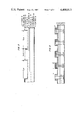
- FIG. 1 is a pictorial view of a semiconductor laser constructed in accordance with the present invention.
- FIGS. 2 and 3 are cross sectional views of the semiconductor laser shown in FIG. 1.
- the embodiment which was constructed in accordance with the present invention uses a ridge-type structure in order to achieve lateral mode confinement in a laser that operates at a wavelength of about 1.55 micrometers.
- a similar laser with a continuous ridge is disclosed in the article entitled "Single-Mode C.W. Ridge-Waveguide Laser Emitting At 1.55 ⁇ m,” by I. P. Kaminow et al., Electronics Letters, Nov. 8, 1979, Vol. 15, No. 23, pp. 763-765.
- the laser constructed in accordance with the present invention is similar to the ridge-type laser in the Kaminow et al. article except that the ridge in accordance with the present embodiment is notched along the entire length in order to produce a crenelated-ridge structure.
- a multilayered liquid phase epitaxial structure is constructed by depositing an indium phosphide n-type cladding layer 21 on the ⁇ 100> surface of an n-type indium phosphide substrate 20 as indicated in FIG. 2.
- An undoped indium gallium arsenide phosphide active layer 22 is then grown with a thickness of about 0.3 ⁇ m followed by a p-type indium gallium arsenide phosphide buffer layer 23 grown with a thickness of about 0.3 ⁇ m.
- the buffer layer is then followed by a p-type indium phosphide cladding layer 24 having a thickness of about 1 ⁇ m and a p-type indium gallium arsenide phosphide cap layer 25 grown with a thickness of about 0.5 ⁇ m.
- the lattice-matched quaternary active layer has a bandgap corresponding to 1.55 ⁇ m and the cap and buffer layers each have bandgaps of 1.13 ⁇ m.
- the grown p-type layers are zinc doped and the n-type layers are tin doped. Additional zinc is diffused into the cap layer 25 in order to increase its conductivity.
- the crenelated ridge structure is then constructed by photolithographically creating a mask on the top surface of the wafer which has windows in all of the areas that are to be protected during an ion milling step that follows. Titanium is then deposited through these windows in the areas which will eventually correspond to the topmost regions of the crenelated-ridge structure. Ion milling is then used to erode away the cap layer in regions that are 20 micrometers wide on each side of the ridge structure and in the notches that are between the teeth of the crenelated-ridge structure.
- the mask is constructed so that a 10 micrometer wide ridge is notched along its length with a periodicity of 10 micrometers ( ⁇ ) thereby causing each tooth of the ridge to be 5 micrometers long and 10 micrometers wide with a spacing of 5 micrometers between adjacent teeth.
- an HCl-H 3 PO 4 stop etch is used to remove the remainder of the indium phosphide cladding layer 24 up to the quaternary buffer layer 23.
- This process produces well-defined teeth in the crenelated ridge structure with near vertical walls giving an appearance for each semiconductor laser 10 of the type illustrated in FIG. 1.
- the titanium mask is then removed with an HF acid etch.
- a 0.3 micrometer thick silicon dioxide insulating layer 26 is sputtered over the entire surface taking care to cover all of the exposed sides of the teeth and the exposed quaternary buffer layer 23. Then a photoresist mask is created with windows over the tops of each of the teeth in the crenelated ridge structure. A plasma etch is used to remove the insulating layer in the windows. The photoresist is then washed away with solvent. A Ti-Sn layer is evaporated over the SiO 2 layer 26 and a thin gold layer is then evaporated over the Ti-Sn layer to create electrode 27.
- Electrode 28 is coated over the bottom surface of the wafer and alloyed thereby creating electrode 28 on the bottom surface of the wafer, and an electroplated gold pad (not shown in the drawing) approximately 10 micrometers thick is deposited over the entire electrode structure 27 in FIG. 1.
- each ridge period ⁇ will contain an integral number of half guide wavelengths when the condition above is satisfied. This fact can be expressed by the following equation:
- ⁇ is the optical wavelength
- n is the index of refraction of the active medium
- m is an integer.
- the indium gallium arsenide phosphide system has a gain width of about 150 A. Assuming that the laser may be subjected to temperature variations of 40 degrees C. and that the gain peak can be shifted by about 4 A/C, the peak can be tuned over a range of about 160 A. Accordingly, the total lasing range for a laser in this material system is about 300 A. As indicated in the above table using an electrode structure with a period of 5 ⁇ m, there is a rather low probability that the laser can be made to oscillate with a guide half-wavelength equal to a sub-harmonic of ⁇ . A ridge structure having a period of 20 micrometers on the other hand will certainly satisfy Eq. (1) once or twice somewhere within the range of lasing wavelengths.
Landscapes
- Physics & Mathematics (AREA)
- Condensed Matter Physics & Semiconductors (AREA)
- General Physics & Mathematics (AREA)
- Electromagnetism (AREA)
- Optics & Photonics (AREA)
- Geometry (AREA)
- Semiconductor Lasers (AREA)
Abstract
Description
Λ=mλ/2n (1)
∂λ/∂m=λ.sup.2 /2nΛ(2)
______________________________________
        Λ
              ∂λ
______________________________________
        5 μm
              720 A
        10 μmm
              360 A
        20 μm
              180 A
______________________________________
Claims (8)
Priority Applications (1)
| Application Number | Priority Date | Filing Date | Title |
|---|---|---|---|
| US06/285,253 US4400813A (en) | 1981-07-20 | 1981-07-20 | Crenelated-ridge waveguide laser |
Applications Claiming Priority (1)
| Application Number | Priority Date | Filing Date | Title |
|---|---|---|---|
| US06/285,253 US4400813A (en) | 1981-07-20 | 1981-07-20 | Crenelated-ridge waveguide laser |
Publications (1)
| Publication Number | Publication Date |
|---|---|
| US4400813A true US4400813A (en) | 1983-08-23 |
Family
ID=23093444
Family Applications (1)
| Application Number | Title | Priority Date | Filing Date |
|---|---|---|---|
| US06/285,253 Expired - Lifetime US4400813A (en) | 1981-07-20 | 1981-07-20 | Crenelated-ridge waveguide laser |
Country Status (1)
| Country | Link |
|---|---|
| US (1) | US4400813A (en) |
Cited By (13)
| Publication number | Priority date | Publication date | Assignee | Title |
|---|---|---|---|---|
| EP0156566A1 (en) * | 1984-03-12 | 1985-10-02 | BRITISH TELECOMMUNICATIONS public limited company | Semiconductor devices |
| WO1985005504A1 (en) * | 1984-05-24 | 1985-12-05 | American Telephone & Telegraph Company | Method of making heteroepitaxial ridge overgrown laser |
| US4573163A (en) * | 1982-09-13 | 1986-02-25 | At&T Bell Laboratories | Longitudinal mode stabilized laser |
| US4720836A (en) * | 1984-09-28 | 1988-01-19 | Hitachi, Ltd. | Distributed feedback semiconductor laser |
| US4830986A (en) * | 1985-05-15 | 1989-05-16 | Itt Corporation | Laser manufacture |
| DE3923354A1 (en) * | 1989-07-14 | 1991-01-24 | Licentia Gmbh | SEMICONDUCTOR LASER |
| US5243669A (en) * | 1992-04-07 | 1993-09-07 | At&T Bell Laboratories | Asymmetric, periodically loaded waveguide for polarization rotation |
| WO1996037933A1 (en) * | 1995-05-23 | 1996-11-28 | Antoine Labeyrie | Laser transmitting or receiving devices and method, for optically transmitting information |
| US5770468A (en) * | 1993-01-12 | 1998-06-23 | Mitsubishi Denki Kabushiki Kaisha | Process for mounting a semiconductor chip to a chip carrier by exposing a solder layer to a reducing atmosphere |
| US20040081214A1 (en) * | 2002-10-24 | 2004-04-29 | Mawst Luke J. | Narrow lateral waveguide laser |
| WO2011012100A1 (en) * | 2009-07-31 | 2011-02-03 | Osram Opto Semiconductors Gmbh | Broad area laser having an epitaxial stack of layers and method for the production thereof |
| JP2018518053A (en) * | 2015-06-05 | 2018-07-05 | ザ ガバメント オブ ザ ユナイテッド ステイツ オブ アメリカ,アズ リプレゼンテッド バイ ザ セクレタリー オブ ザ ネイビー | Inter-band cascade laser with low fill factor top contact to reduce losses |
| US11133649B2 (en) * | 2019-06-21 | 2021-09-28 | Palo Alto Research Center Incorporated | Index and gain coupled distributed feedback laser |
Citations (4)
| Publication number | Priority date | Publication date | Assignee | Title |
|---|---|---|---|---|
| US3760292A (en) * | 1970-12-22 | 1973-09-18 | Bell Telephone Labor Inc | Integrated feedback laser |
| US3891302A (en) * | 1973-09-28 | 1975-06-24 | Western Electric Co | Method of filtering modes in optical waveguides |
| US4257011A (en) * | 1977-08-01 | 1981-03-17 | Hitachi, Ltd. | Semiconductor laser device |
| US4375686A (en) * | 1979-12-13 | 1983-03-01 | U.S. Philips Corporation | Semiconductor laser |
-
1981
- 1981-07-20 US US06/285,253 patent/US4400813A/en not_active Expired - Lifetime
Patent Citations (4)
| Publication number | Priority date | Publication date | Assignee | Title |
|---|---|---|---|---|
| US3760292A (en) * | 1970-12-22 | 1973-09-18 | Bell Telephone Labor Inc | Integrated feedback laser |
| US3891302A (en) * | 1973-09-28 | 1975-06-24 | Western Electric Co | Method of filtering modes in optical waveguides |
| US4257011A (en) * | 1977-08-01 | 1981-03-17 | Hitachi, Ltd. | Semiconductor laser device |
| US4375686A (en) * | 1979-12-13 | 1983-03-01 | U.S. Philips Corporation | Semiconductor laser |
Non-Patent Citations (7)
| Title |
|---|
| de Waard, "A Novel Single Mode Laser Having Periodic Variations in the Stripe Width," Proceedings of Optical Comm. Conf., Amsterdam, Netherlands, Sep. 17-19, 1979, pp. 1-11. * |
| Doi et al., "InGaAsP/InP Distributed-Feedback Injection Lasers Fabricated by One-Step Liquid Phase Epitaxy," Sep. 15, 1979, Appl. Phys. Lett. vol. 35, No. 6, pp. 441-443. * |
| Kaminow et al., "Single-Mode C. W. Ridge-Waveguide Laser Emitting at 1.55 pm, " Elect. Lett. vol. 15, No. 23, Nov. 8, 1979, pp. 73-74. * |
| Lasher, "Analysis of a Proposed Bistable Injection Laser," 1964, Solid-State Elect., vol. 7, pp. 707-716. * |
| Lee et al., "Repetitively Q-Switched Light Pulses from GaAs Injection Lasers with Tandem Double-Section Stripe Geometry," IEEE J. of Quant. Elect. vol. QE-6, No. 6, Jun. 1970, pp. 339-352. * |
| Nathan et al, "GaAs Injection Laser with Novel Mode Control and Switching Properties," Feb. 1965, J. Appl. Phys., vol. 36, No. 2, pp. 473-480. * |
| Shubert, "Theory of Optical-Waveguide Distributed Lasers with Nonuniform Gain and Coupling," J. Appl. Phys. Jan. 1974, vol. 45, No. 1, pp. 209-216. * |
Cited By (22)
| Publication number | Priority date | Publication date | Assignee | Title |
|---|---|---|---|---|
| US4573163A (en) * | 1982-09-13 | 1986-02-25 | At&T Bell Laboratories | Longitudinal mode stabilized laser |
| EP0156566A1 (en) * | 1984-03-12 | 1985-10-02 | BRITISH TELECOMMUNICATIONS public limited company | Semiconductor devices |
| US4805184A (en) * | 1984-03-12 | 1989-02-14 | British Telecommunications, Plc | Ridge waveguide optical devices |
| WO1985005504A1 (en) * | 1984-05-24 | 1985-12-05 | American Telephone & Telegraph Company | Method of making heteroepitaxial ridge overgrown laser |
| US4720836A (en) * | 1984-09-28 | 1988-01-19 | Hitachi, Ltd. | Distributed feedback semiconductor laser |
| US4830986A (en) * | 1985-05-15 | 1989-05-16 | Itt Corporation | Laser manufacture |
| DE3923354A1 (en) * | 1989-07-14 | 1991-01-24 | Licentia Gmbh | SEMICONDUCTOR LASER |
| US5243669A (en) * | 1992-04-07 | 1993-09-07 | At&T Bell Laboratories | Asymmetric, periodically loaded waveguide for polarization rotation |
| US5770468A (en) * | 1993-01-12 | 1998-06-23 | Mitsubishi Denki Kabushiki Kaisha | Process for mounting a semiconductor chip to a chip carrier by exposing a solder layer to a reducing atmosphere |
| FR2734676A1 (en) * | 1995-05-23 | 1996-11-29 | Labeyrie Antoine | LASER EMISSION OR RECEPTION METHOD AND DEVICES FOR OPTICAL TRANSMISSION OF INFORMATION |
| WO1996037933A1 (en) * | 1995-05-23 | 1996-11-28 | Antoine Labeyrie | Laser transmitting or receiving devices and method, for optically transmitting information |
| US6044102A (en) * | 1995-05-23 | 2000-03-28 | Labeyrie; Antoine | Laser transmitting or receiving devices and method for optically transmitting information |
| US20040081214A1 (en) * | 2002-10-24 | 2004-04-29 | Mawst Luke J. | Narrow lateral waveguide laser |
| US6845116B2 (en) | 2002-10-24 | 2005-01-18 | Wisconsin Alumni Research Foundation | Narrow lateral waveguide laser |
| CN102474078A (en) * | 2009-07-31 | 2012-05-23 | 奥斯兰姆奥普托半导体有限责任公司 | Wide stripe laser with epitaxial layer stack and method of manufacturing the same |
| WO2011012100A1 (en) * | 2009-07-31 | 2011-02-03 | Osram Opto Semiconductors Gmbh | Broad area laser having an epitaxial stack of layers and method for the production thereof |
| JP2013501347A (en) * | 2009-07-31 | 2013-01-10 | オスラム オプト セミコンダクターズ ゲゼルシャフト ミット ベシュレンクテル ハフツング | Broad area laser with epitaxial laminate and method for manufacturing broad area laser |
| US8619833B2 (en) | 2009-07-31 | 2013-12-31 | Osram Opto Semiconductors Gmbh | Broad area laser having an epitaxial stack of layers and method for the production thereof |
| CN102474078B (en) * | 2009-07-31 | 2014-09-17 | 奥斯兰姆奥普托半导体有限责任公司 | Wide stripe laser with epitaxial layer stack and method of manufacturing the same |
| JP2018518053A (en) * | 2015-06-05 | 2018-07-05 | ザ ガバメント オブ ザ ユナイテッド ステイツ オブ アメリカ,アズ リプレゼンテッド バイ ザ セクレタリー オブ ザ ネイビー | Inter-band cascade laser with low fill factor top contact to reduce losses |
| US11133649B2 (en) * | 2019-06-21 | 2021-09-28 | Palo Alto Research Center Incorporated | Index and gain coupled distributed feedback laser |
| US20210391692A1 (en) * | 2019-06-21 | 2021-12-16 | Palo Alto Research Center Incorporated | Index and gain coupled distributed feedback laser |
Similar Documents
| Publication | Publication Date | Title |
|---|---|---|
| US5147825A (en) | Photonic-integrated-circuit fabrication process | |
| US4503540A (en) | Phase-locked semiconductor laser device | |
| US4728628A (en) | Method of making ridge waveguide lasers | |
| US4257011A (en) | Semiconductor laser device | |
| EP0375021B1 (en) | Tunable semiconductor diode laser with distributed reflection and method of manufacturing such a semiconductor diode laser | |
| CA1150810A (en) | Semiconductor laser device | |
| US4400813A (en) | Crenelated-ridge waveguide laser | |
| JPH0666509B2 (en) | Distributed feedback semiconductor laser device | |
| US4775980A (en) | Distributed-feedback semiconductor laser device | |
| US4575851A (en) | Double channel planar buried heterostructure laser with periodic structure formed in guide layer | |
| JPH0582889A (en) | Semiconductor laser and manufacturing method thereof | |
| US4674096A (en) | Lateral coupled cavity semiconductor laser | |
| US4488307A (en) | Three-mirror active-passive semiconductor laser | |
| EP0187718B1 (en) | A distributed feedback semiconductor laser device | |
| GB2112201A (en) | Constricted double heterostructure semiconductor laser | |
| EP0206745B1 (en) | A semiconductor laser apparatus | |
| KR20030069879A (en) | Method of producing a semiconductor laser and optical integrated semiconductor device including the same | |
| JPS6328520B2 (en) | ||
| US5027368A (en) | Semiconductor laser device | |
| US5105431A (en) | Semiconductor laser | |
| US20050078724A1 (en) | Single mode distributed feedback lasers | |
| JPS6329596A (en) | Semiconductor laser | |
| JPS58158988A (en) | Distributed feedback type semiconductor laser | |
| JPS60165782A (en) | Semiconductor laser | |
| EP1309050A1 (en) | Laser device and method therefor |
Legal Events
| Date | Code | Title | Description |
|---|---|---|---|
| AS | Assignment |
Owner name: BELL TELEPHONE LABORATORIES INCORPORATED, 600 MOUN Free format text: ASSIGNMENT OF ASSIGNORS INTEREST.;ASSIGNOR:KAMINOW, IVAN P.;REEL/FRAME:003901/0280 Effective date: 19810717 |
|
| STCF | Information on status: patent grant |
Free format text: PATENTED CASE |
|
| MAFP | Maintenance fee payment |
Free format text: PAYMENT OF MAINTENANCE FEE, 4TH YEAR, PL 96-517 (ORIGINAL EVENT CODE: M170); ENTITY STATUS OF PATENT OWNER: LARGE ENTITY Year of fee payment: 4 |
|
| FEPP | Fee payment procedure |
Free format text: PAYOR NUMBER ASSIGNED (ORIGINAL EVENT CODE: ASPN); ENTITY STATUS OF PATENT OWNER: LARGE ENTITY |
|
| MAFP | Maintenance fee payment |
Free format text: PAYMENT OF MAINTENANCE FEE, 8TH YEAR, PL 96-517 (ORIGINAL EVENT CODE: M171); ENTITY STATUS OF PATENT OWNER: LARGE ENTITY Year of fee payment: 8 |
|
| MAFP | Maintenance fee payment |
Free format text: PAYMENT OF MAINTENANCE FEE, 12TH YEAR, LARGE ENTITY (ORIGINAL EVENT CODE: M185); ENTITY STATUS OF PATENT OWNER: LARGE ENTITY Year of fee payment: 12 |