US4397014A - Bidirectional pulse generator for video disc stylus deflector transducer - Google Patents
Bidirectional pulse generator for video disc stylus deflector transducer Download PDFInfo
- Publication number
- US4397014A US4397014A US06/290,498 US29049881A US4397014A US 4397014 A US4397014 A US 4397014A US 29049881 A US29049881 A US 29049881A US 4397014 A US4397014 A US 4397014A
- Authority
- US
- United States
- Prior art keywords
- amplifier
- potential
- inverting
- inverting input
- signal
- Prior art date
- Legal status (The legal status is an assumption and is not a legal conclusion. Google has not performed a legal analysis and makes no representation as to the accuracy of the status listed.)
- Expired - Lifetime
Links
- 230000002457 bidirectional effect Effects 0.000 title claims abstract description 11
- 239000003990 capacitor Substances 0.000 claims description 12
- 230000001143 conditioned effect Effects 0.000 claims description 3
- 238000005513 bias potential Methods 0.000 claims description 2
- 238000007599 discharging Methods 0.000 claims 1
- 230000003750 conditioning effect Effects 0.000 abstract description 2
- 230000007704 transition Effects 0.000 description 8
- 241001422033 Thestylus Species 0.000 description 4
- 230000014616 translation Effects 0.000 description 3
- 238000013519 translation Methods 0.000 description 3
- 238000010586 diagram Methods 0.000 description 2
- 230000000644 propagated effect Effects 0.000 description 2
- 241000630329 Scomberesox saurus saurus Species 0.000 description 1
- 230000002547 anomalous effect Effects 0.000 description 1
- 230000000295 complement effect Effects 0.000 description 1
- 239000002131 composite material Substances 0.000 description 1
- 239000013078 crystal Substances 0.000 description 1
- 230000000694 effects Effects 0.000 description 1
- 230000001747 exhibiting effect Effects 0.000 description 1
- 102220170674 rs112939575 Human genes 0.000 description 1
Images
Classifications
-
- G—PHYSICS
- G11—INFORMATION STORAGE
- G11B—INFORMATION STORAGE BASED ON RELATIVE MOVEMENT BETWEEN RECORD CARRIER AND TRANSDUCER
- G11B21/00—Head arrangements not specific to the method of recording or reproducing
- G11B21/02—Driving or moving of heads
-
- H—ELECTRICITY
- H03—ELECTRONIC CIRCUITRY
- H03K—PULSE TECHNIQUE
- H03K4/00—Generating pulses having essentially a finite slope or stepped portions
- H03K4/06—Generating pulses having essentially a finite slope or stepped portions having triangular shape
- H03K4/08—Generating pulses having essentially a finite slope or stepped portions having triangular shape having sawtooth shape
- H03K4/48—Generating pulses having essentially a finite slope or stepped portions having triangular shape having sawtooth shape using as active elements semiconductor devices
- H03K4/60—Generating pulses having essentially a finite slope or stepped portions having triangular shape having sawtooth shape using as active elements semiconductor devices in which a sawtooth current is produced through an inductor
- H03K4/69—Generating pulses having essentially a finite slope or stepped portions having triangular shape having sawtooth shape using as active elements semiconductor devices in which a sawtooth current is produced through an inductor using a semiconductor device operating as an amplifier
- H03K4/72—Generating pulses having essentially a finite slope or stepped portions having triangular shape having sawtooth shape using as active elements semiconductor devices in which a sawtooth current is produced through an inductor using a semiconductor device operating as an amplifier combined with means for generating the driving pulses
- H03K4/725—Push-pull amplifier circuits
-
- H—ELECTRICITY
- H03—ELECTRONIC CIRCUITRY
- H03K—PULSE TECHNIQUE
- H03K4/00—Generating pulses having essentially a finite slope or stepped portions
- H03K4/94—Generating pulses having essentially a finite slope or stepped portions having trapezoidal shape
Definitions
- This invention relates to pulse generators and in particular to a circuit for producing bidirectional pulses.
- Bidirectional pulse generators of the type described herein have been found useful for driving a video disc stylus deflector transducer.
- Certain video disc player systems employ a track following signal pickup stylus for recovering prerecorded information from information-bearing tracks disposed on a record disc.
- the stylus is secured to a stylus arm which is compliantly mounted in an arm carriage assembly for translating the stylus/stylus arm radially across the disc in synchronism with the rate of advance of the information due to rotation of the disc.
- a stylus deflector is incorporated with the carriage and stylus arm to correct for anomalous radial stylus movement (inward or outward) or to produce special effects such as stop motion, slow motion, record preview, etc.
- a typical deflector transducer comprises a permanent magnet secured to the stylus arm disposed between two electromagnetic coils secured to the carriage assembly. Energizing the coils produces a magnetic field therebetween to induce a relatively precise translation of the permanent magnet and thereby a radial translation of the stylus/stylus arm. See for example U.S. Pat. No. 4,262,174, filed May 15, 1979, by J. C. Bleazey and entitled, "Track Skipper for Video Disc" assigned to the common assignee with this invention.
- the present invention is a circuit suitable for producing energizing pulses for the deflector coils capable of providing stylus translations or deflections of varying distance in both the inward and outward radial direction.
- a waveform generator responsive to a first control signal generates a signal having a prescribed waveshape, the amplitude of which being proportional to the duration of the first control signal.
- Signal from the waveform generator is selectively applied to either the inverting or non-inverting input terminal of a differential amplifier depending upon the desired polarity of drive signal.
- the amplifier input terminal signal selection is controlled by a second control signal whch concurrently establishes the quiescent bias potentials of the amplifier input terminals and thereby the amplifier output quiescent potential. For example, if a negative-going drive pulse is desired the second control signal conditions the amplifier non-inverting input terminal potential bias at a relatively high potential and conditions the inverting input terminal to receive signal from the waveform generator.
- the amplifier quiescent output potential assumes a relatively high potential responsive to such bias and upon the occurrence of a first control signal pulse the signal applied by the waveform generator to the inverting input terminal is amplified and inverted at the amplifier output.
- the amplifier output potential goes through a negative excursion from the relatively high quiescent potential tending toward the relatively low supply potential.
- the second control signal conditions the bias at the non-inverting input terminal relatively low (and thereby the amplifier output quiescent potential low) and conditions the non-inverting input terminal to receive signal from the waveform generator. In this case the output drive signal excursion is positive going, from the relatively low quiescent output potential toward the relatively high supply potential.
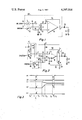
- FIGS. 1 and 2 are circuit schematic diagrams of bidirectional pulse generators embodying the present invention.
- FIG. 3 is a time versus voltage waveform diagram relating the output potential of the FIG. 2 circuit to the applied control voltages.
- a transducer 22 e.g., an electromagnetic coil, piezoelectric crystal, etc.
- Capacitor 23 serves the purpose of isolating the DC potential at connection 13 from the transducer 22 so that positive-going signals and negative-going signals with prescribed minimum frequency components are coupled to the transducer having an average DC potential about reference potential 20.
- the pulse generator 100 is responsive to two control signals, a deflection pulse applied to terminal 18 and a direction signal applied to terminal 19. In normal operation, transitions of the two control signals do not occur simultaneously but rather the state of the direction signal is established with the pulse generator response thereto completed before the occurrence of a deflection pulse.
- a differential amplifier 10 has a non-inverting input connection 15 connected to the output terminal 16 of waveform generator 11 by a resistor R4 and connected to reference potential 20 by resistor R5.
- An inverting input connection 14 of the differential amplifier 10 is connected to waveform generator 11 by the serially connected resistors R2 and R3 and is connected to the output connection 13 by feedback resistor R1.
- a first diode D1 connects the intersection of resistors R2 and R3 to the direction signal buffer circuit 12 and a second diode D2 connects the non-inverting input connection 15 of amplifier 10 to circuit 12.
- the output impedance of both the waveform generator 11 and the direction signal buffer circuit 12 are relatively low compared to the resistances of R3 and R4.
- the direction signal applied to terminal 19 is one of two levels, high or low. These levels are buffered by circuit 12 to produce a signal which is applied to the interconnection 21 of diodes D1 and D2.
- diode D2 In the presence of a relatively high potential at connection 21, diode D2 is conditioned to conduct thereby imposing the relatively high potential at connection 21 on the non-inverting input connection 15 (less a forward diode drop). Concurrently diode D1 is reverse biased or cut off effectively eliminating it from the circuit.
- terminal 16 is substantially at reference potential, configuring the circuit as a non-inverting amplifier with a relatively high DC potential signal at its input, and exhibiting a DC gain at its output terminal 13 of (1+R1/(R2+R3)) producing a relatively high output potential where R1, R2 and R3 are the respective resistance values of the corresponding resistors.
- a deflection pulse to terminal 18 conditions the waveform generator 11 to output a positive-going pulse of prescribed amplitude and waveshape to terminal 16, which pulse is coupled by resistors R2 and R3 to the inverting input connection 14 of amplifier 10.
- the pulse applied to terminal 16 is precluded from modulating the non-inverting input connection 15 by the clamping action of forward-biased diode D2.
- the amplifier 10 inverts the sense of the pulse applied to its inverting input.
- the pulse is propagated through the amplifier appearing at the output connection 13 inverted and modified by the gain factor R1/(R2+R3).
- the output pulse at connection 13 commences at the relative high DC level established by the direction signal and tends toward the opposite or relatively low supply potential.
- connection 15 is pulled near reference potential, e.g., ground, by the conduction path provided by resistor R5.
- the potential offset of the amplifier is arranged so that under these circumstances the output potential, though relatively low, when translated back by the resistors R1 and R2 is sufficient to condition diode D1 to conduct.
- a deflection pulse such pulse is precluded from modulating the inverting input connection 14 by the clamping action of diode D1, but is coupled to the non-inverting input connection 15 by resistor R4.
- the pulse is propagated to the output non-inverted, and modified by the gain factor (1+R1/R2).
- the output pulse at connection 13 commences at the relatively low DC potential established by the low direction signal and goes through an excursion tending toward the positive or relatively high supply potential.
- amplifier 30 driving complementary transistor emitter followers Q1 and Q2 forms a composite differential amplifier 60 with negative feedback provided by resistor R10.
- the output signal at connection 40 from amplifier 60 is coupled via capacitor C2 to a transducer 22.
- a direction signal buffer circuit 12' comprising transistor Q4 and resistors R14 and R18 is responsive to a bilevel direction signal applied to terminal 49 to generate a potential for selectively conditioning diodes D1 and D2 to conduct.
- a low potential signal applied to terminal 49 conditions Q4 to be non-conducting so that the potential at interconnection 41 is determined by the ratio R14/(R14+R18) times the value of the supply potential V.
- the potential at interconnection 41 is relatively high where R14 and R18 are the respective resistance values of the corresponding resistors.
- transistor Q4 to conduct essentially clamping interconnection 41 to ground potential, i.e., a relatively low potential.
- the dynamic impedance looking into the buffer circuit 12' from interconnection 41 is the saturation resistance of Q4 when conducting, or the impedance of the parallel connection of resistors R18 and R14, i.e. R18 ⁇ R14/(R18+R14), the latter impedance being substantially smaller than the resistance of resistor R13.
- application of DC potentials to the interconnection of the diodes selectively establishes the DC bias of the amplifier and determines which of the inverting and non-inverting amplifier input terminals receives signal applied by waveform generator 11'.
- Waveform generator 11' comprises transistor Q3, resistors R17, R19 and capacitor C1.
- the resistance of R19 is small compared to the resistance of R17 and is included to improve the fall time at terminal 42 and to limit dissipation in transistor Q3 when it conducts initially to discharge capacitor C1.
- the potential at input terminal 48 is normally sufficiently high to condition transistor Q3 to be conducting in saturation, thereby grounding terminal 42.
- the potential at connection 43 discharges through resistor R19 to a value V1 equal to R19/(R17+R19) times V supply.
- Such charging produces a fairly linear positive going ramp potential signal for a relatively large portion of the potential excursion from potential V1 to V supply.
- the potential V43 at connection 43 is approximated by:
- R17 and C1 are the respective resistance and capacitance values of the corresponding devices and from which it can be seen that the longer the duration of time t the larger the amplitude of potential V43.
- the time t corresponds to the duration of the deflection pulse, i.e., the time Q3 is non-conducting.
- the potential V43 is coupled via resistor R19 to the terminal 42 from which it is applied to the non-inverting terminal 46 or inverting terminal 45 of amplifier 30 depending on which diode is conducting.
- the resistors R16 and R15 form a potential divider to bias connection 46 slightly positive for diode D2 non-conducting. This potential is chosen such that when amplified by amplifier 60 and fed back to connection 44 via resistors R10 and R11 it conditions diode D1 to conduct. Thus for connection 46 at a relatively low potential, diode D1 is forward biased and clamps the input signal to the inverting signal terminal 45 at a DC potential.
- waveform 3(a) corresponds to the deflection pulse applied to terminal 48
- waveform 3(b) is the potential produced at terminal 42.
- transistor Q3 is conducting and terminal 42 is clamped to ground.
- the deflection pulses goes negative turning off transistor Q3 and allowing connection 43 and thereby terminal 42 to charge toward the positive supply potential, the longer the charging time the higher the resulting potential, as demonstrated by the broken lines in the figure.
- the deflection pulse terminates, transistor Q3 again conducts and terminal 42 is clamped to ground.
- the potential at terminal 42 is applied to the amplifier non-inverting input terminal 46 with a positive-going signal appearing at output connection 40 (waveform 3(d)) which is coupled by capacitor C2 to transducer 22 (waveform 3(e)).
- Waveform 3(c) represents the direction signal applied to terminal 49.
- transistor Q4 conducts and node 41 is low with the consequence of biasing the ouput at connection 40 low.
- the direction pulse is going through a transition from high toward low, turning Q4 off, and biasing connection 46 relatively high, etc. From waveform 3(d) it is seen that the subsequent deflection signal at node 42 is inverted (time T6-T7).
- the transition (T4-T5) of the direction signal is relatively long compared with the signal transition (T6-T7) to prevent the DC potential transition at connection 40 from being coupled in sufficient amplitude by capacitor C2 to energize the transducer 22.
- Table 1 is a list of device values for a particular realization of the FIG. 2 circuit.
Landscapes
- Details Of Television Scanning (AREA)
Abstract
Description
V43=V supply (1-exp(-t/R17C1)) (1)
              TABLE 1
______________________________________
Resistor       Resistance
______________________________________
R10            100K Ohm
R11             15K Ohm
R12             51K Ohm
R13            330K Ohm
R14             10K Ohm
R15            110K Ohm
R16            1.3M Ohm
R17             15K Ohm
R18             12K Ohm
R19             1K Ohm
Capacitor      Capacitance
Cl             0.1μ Farad
Diode D1, D2   IN914
Transistors Q3, Q4
               MPSA17             Motorola
Transistor Q1  MPSU01             transistors
Transistor Q2  MPSU51
Amplifier 30   CA324
______________________________________
Claims (6)
Priority Applications (1)
| Application Number | Priority Date | Filing Date | Title |
|---|---|---|---|
| US06/290,498 US4397014A (en) | 1979-11-28 | 1981-08-06 | Bidirectional pulse generator for video disc stylus deflector transducer |
Applications Claiming Priority (2)
| Application Number | Priority Date | Filing Date | Title |
|---|---|---|---|
| US9824379A | 1979-11-28 | 1979-11-28 | |
| US06/290,498 US4397014A (en) | 1979-11-28 | 1981-08-06 | Bidirectional pulse generator for video disc stylus deflector transducer |
Related Parent Applications (1)
| Application Number | Title | Priority Date | Filing Date |
|---|---|---|---|
| US9824379A Continuation | 1979-11-19 | 1979-11-28 |
Publications (1)
| Publication Number | Publication Date |
|---|---|
| US4397014A true US4397014A (en) | 1983-08-02 |
Family
ID=26794484
Family Applications (1)
| Application Number | Title | Priority Date | Filing Date |
|---|---|---|---|
| US06/290,498 Expired - Lifetime US4397014A (en) | 1979-11-28 | 1981-08-06 | Bidirectional pulse generator for video disc stylus deflector transducer |
Country Status (1)
| Country | Link |
|---|---|
| US (1) | US4397014A (en) |
-
1981
- 1981-08-06 US US06/290,498 patent/US4397014A/en not_active Expired - Lifetime
Similar Documents
| Publication | Publication Date | Title |
|---|---|---|
| US3959817A (en) | Switching circuit for connecting a magnetic head in a magnetic recording and reproducing apparatus | |
| US4338529A (en) | Cue signal generating circuit | |
| JP3623963B2 (en) | Information signal recording device | |
| US3568094A (en) | Pulse width modulator | |
| US4397014A (en) | Bidirectional pulse generator for video disc stylus deflector transducer | |
| JPS59123321A (en) | Switch circuit | |
| CA1149948A (en) | Bidirectional pulse generator for video disc stylus deflector transducer | |
| JPS6055905B2 (en) | Piezoelectric element control device for positioning | |
| US5894237A (en) | Write driver with buffer circuits between pull-up resistors and upper drive transistors | |
| US4868691A (en) | Recording or reproducing apparatus | |
| US5677647A (en) | High power pulse waveform generator | |
| US4533965A (en) | Magnetic read/write circuit | |
| US4750061A (en) | Amplitude limiter circuit | |
| GB2064252A (en) | Bidirectional pulse generator | |
| US3143658A (en) | Method and apparatus for producing and recording a pulse frequency modulated signal | |
| US3797038A (en) | Data or audio recording and playback apparatus | |
| US4313062A (en) | Bidirectional deflector driver for video disc | |
| US3550117A (en) | Timing apparatus | |
| US4254346A (en) | Monostable multivibrator | |
| US3441747A (en) | Detector for bipolar digital signals | |
| US3261004A (en) | Read-write amplifier circuit | |
| US3438054A (en) | Write driver circuit for a digital magnetic recording head | |
| US2682578A (en) | Demagnetization system for magnetic recorder-reproducer | |
| US3056119A (en) | Recording circuit | |
| KR0182968B1 (en) | Flip-flop buffer circuit of hard disk driver |
Legal Events
| Date | Code | Title | Description |
|---|---|---|---|
| STCF | Information on status: patent grant |
Free format text: PATENTED CASE |
|
| CC | Certificate of correction | ||
| MAFP | Maintenance fee payment |
Free format text: PAYMENT OF MAINTENANCE FEE, 4TH YEAR, PL 96-517 (ORIGINAL EVENT CODE: M170); ENTITY STATUS OF PATENT OWNER: LARGE ENTITY Year of fee payment: 4 |
|
| FEPP | Fee payment procedure |
Free format text: MAINTENANCE FEE REMINDER MAILED (ORIGINAL EVENT CODE: REM.); ENTITY STATUS OF PATENT OWNER: LARGE ENTITY |
|
| FEPP | Fee payment procedure |
Free format text: SURCHARGE FOR LATE PAYMENT, PL 96-517 (ORIGINAL EVENT CODE: M176); ENTITY STATUS OF PATENT OWNER: LARGE ENTITY |
|
| MAFP | Maintenance fee payment |
Free format text: PAYMENT OF MAINTENANCE FEE, 8TH YEAR, PL 96-517 (ORIGINAL EVENT CODE: M171); ENTITY STATUS OF PATENT OWNER: LARGE ENTITY Year of fee payment: 8 |
|
| MAFP | Maintenance fee payment |
Free format text: PAYMENT OF MAINTENANCE FEE, 12TH YEAR, LARGE ENTITY (ORIGINAL EVENT CODE: M185); ENTITY STATUS OF PATENT OWNER: LARGE ENTITY Year of fee payment: 12 |