US4051473A - Input tracking threshold detector - Google Patents
Input tracking threshold detector Download PDFInfo
- Publication number
- US4051473A US4051473A US05/727,112 US72711276A US4051473A US 4051473 A US4051473 A US 4051473A US 72711276 A US72711276 A US 72711276A US 4051473 A US4051473 A US 4051473A
- Authority
- US
- United States
- Prior art keywords
- signal
- detector
- radar system
- circuit
- receiving
- Prior art date
- Legal status (The legal status is an assumption and is not a legal conclusion. Google has not performed a legal analysis and makes no representation as to the accuracy of the status listed.)
- Expired - Lifetime
Links
- 238000001514 detection method Methods 0.000 description 5
- 230000035945 sensitivity Effects 0.000 description 5
- 230000004048 modification Effects 0.000 description 4
- 238000012986 modification Methods 0.000 description 4
- 238000010586 diagram Methods 0.000 description 3
- 230000000694 effects Effects 0.000 description 3
- 230000002452 interceptive effect Effects 0.000 description 2
- 208000019300 CLIPPERS Diseases 0.000 description 1
- 238000006424 Flood reaction Methods 0.000 description 1
- 230000032683 aging Effects 0.000 description 1
- 208000021930 chronic lymphocytic inflammation with pontine perivascular enhancement responsive to steroids Diseases 0.000 description 1
- 230000007423 decrease Effects 0.000 description 1
- 230000003247 decreasing effect Effects 0.000 description 1
- 230000003111 delayed effect Effects 0.000 description 1
- 230000007613 environmental effect Effects 0.000 description 1
- 239000000284 extract Substances 0.000 description 1
- 238000002955 isolation Methods 0.000 description 1
- 238000010606 normalization Methods 0.000 description 1
- 230000001360 synchronised effect Effects 0.000 description 1
- 230000001960 triggered effect Effects 0.000 description 1
Images


Classifications
-
- G—PHYSICS
- G01—MEASURING; TESTING
- G01S—RADIO DIRECTION-FINDING; RADIO NAVIGATION; DETERMINING DISTANCE OR VELOCITY BY USE OF RADIO WAVES; LOCATING OR PRESENCE-DETECTING BY USE OF THE REFLECTION OR RERADIATION OF RADIO WAVES; ANALOGOUS ARRANGEMENTS USING OTHER WAVES
- G01S7/00—Details of systems according to groups G01S13/00, G01S15/00, G01S17/00
- G01S7/02—Details of systems according to groups G01S13/00, G01S15/00, G01S17/00 of systems according to group G01S13/00
- G01S7/28—Details of pulse systems
- G01S7/285—Receivers
- G01S7/292—Extracting wanted echo-signals
- G01S7/2923—Extracting wanted echo-signals based on data belonging to a number of consecutive radar periods
- G01S7/2927—Extracting wanted echo-signals based on data belonging to a number of consecutive radar periods by deriving and controlling a threshold value
-
- G—PHYSICS
- G01—MEASURING; TESTING
- G01S—RADIO DIRECTION-FINDING; RADIO NAVIGATION; DETERMINING DISTANCE OR VELOCITY BY USE OF RADIO WAVES; LOCATING OR PRESENCE-DETECTING BY USE OF THE REFLECTION OR RERADIATION OF RADIO WAVES; ANALOGOUS ARRANGEMENTS USING OTHER WAVES
- G01S7/00—Details of systems according to groups G01S13/00, G01S15/00, G01S17/00
- G01S7/02—Details of systems according to groups G01S13/00, G01S15/00, G01S17/00 of systems according to group G01S13/00
- G01S7/28—Details of pulse systems
- G01S7/285—Receivers
- G01S7/34—Gain of receiver varied automatically during pulse-recurrence period, e.g. anti-clutter gain control
Definitions
- This invention generally relates to electronics and to signal detection. More particularly, in its presently preferred application, this invention relates to a noise tracking threshold detector for a radar system.
- the optimum detection of the radar signal is achieved when the threshold of detection is adjusted such that only a few noise blips appear on the radar display.
- the threshold When the threshold is adjusted lower, noise floods the display obscuring and making indistinguishable any real targets which may be present.
- a noise tracking threshold circuit is frequently used to control the threshold level.
- Previous tracking circuits have been of the analog filter type wherein a long time constant low-pass filter extracts the average value of the receiver noise. This amplitude is then scaled to provide the necessary threshold level to maintain the desired number of noise blips on the display.
- This type of circuit can compensate for variations in receiver gain or voltages by adjusting the threshold accordingly.
- this type of circuit cannot compensate for bandwidth or detector variations and noise distribution changes. Because the circuit cannot compensate for these variations, the maximum sensitivity is not achieved and the system performance is degraded due to environmental conditions and/or aging.
- noise tracking threshold detector which compensates for variations due to voltage shift, gain, bandwidth, noise characteristics, and/or noise distribution.
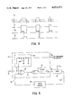
- FIG. 1 is a block circuit diagram illustrating the presently preferred embodiment and application
- FIG. 2 is a circuit diagram illustrating item 11 of FIG. 1 in more detail
- FIGS. 3 and 4 show waveforms useful in explaining the operation of the apparatus of FIGS. 1 and 2, and
- FIG. 5 is a circuit diagram illustrating an alternative implementation of item 11 of FIG. 1.
- threshold detector 11 receives video signal S i produced by the envelope detection of the receiver IF output. Threshold detector 11 also receives a gating signal S g which has predetermined enablement intervals.
- Timing signal generator 13 which comprises conventional frequency dividers driven by a conventional master oscillator, generates S g and the transmitter modulating pulse signal S t . S g and S t are appropriately synchronized with one another.
- Threshold detector 11 comprises a gated output comparison circuit 15 and an integrating circuit 17.
- Circuit 15, which receives S i , the integrator output signal S f , and the gating signal S g , outputs a two-level or binary signal S n which during S g enablement intervals alternates between two levels as a function of the relative amplitudes of S i and S f .
- Circuit 17, from S n produces S f whose amplitude depends on the ratio of S n first level time to S n second level time, i.e., the duty cycle of S n .
- Signal S m the non-gated output of comparison circuit 19, contains the radar return information and may be subjected to further signal processing downstream, or if so desired, S m may be used directly to provide Z-axis modulation for a CRT display.
- S m is one of 3 binary signals which together represent S i in digitized form, and more particularly quantize S i into 4 levels. These 3 binary signals are further processed in a digital processor which is the subject of my U.S. Patent application Ser. No. 720,165 entitled "Radar Signal Processor,” filed Sept. 2, 1976.
- S i is also fed to two non-tracking, comparator-type threshold detectors (not shown) having different threshold levels, both being higher than S f .
- the tracking threshold detector herein is presently employed only on the signal closest to the noise.
- the comparison circuit 19 is seen to comprise a differential input operational amplifier 23 followed by a digital filter 25.
- Op-amp 23 operated as a unipolar output comparator so as to produce a signal S c which is a logic "1" when S i >S f , and a logic of "0" when S i ⁇ S f .
- Digital filter 25 includes a one-shot 27 which when triggered by the op-amp output signal S c outputs at Q a logic "1" pulse and at Q a logic "0" pulse, each of width ⁇ .
- comparison circuit 19 is graphically set forth in FIG. 3 which for purposes of illustration assumes a constant S f level.
- filter 25 is a low-pass filter and prevents contribution by S i to S m unless S i exceeds S f for at least a time slightly greater than ⁇ .
- filter 25 prevents the frequency components in S i which exceed approximately (1/ ⁇ ) Hz from contributing to S m , S n , and thus S f . It is presently preferred that ⁇ be about one half the transmitted pulse width and thus for present embodiments ⁇ is approximately 3 microseconds.
- Gate 21 comprises a NAND gate 31 and a switch 33.
- NAND gate 31 receives S m and S g and drives switch 33 between V volts and ground.
- Switch 33 ensures that in the gate output signal S n , a logic "0" always corresponds to 0 volts and a logic "1" always corresponds to a constant V volts, and thus ensures, as will become more apparent hereinbelow, that the charge and discharge rates of integrating circuit 17 remain constant.
- Switch 33 may be variously embodied and presently comprises a conventional transistor switch.
- Integrating circuit 17 comprises an op-amp type integrator 41, a buffer amplifier 43 and an output attenuation network 45.
- the op-amp integrator 41 is connected to produce different rise and fall rates in S f , the rise rate depending on the value of R a xC, and the fall rate depending on the value of R b xC.
- R a , R b , and C are approximately 22 kilohms, 1 megohm, and 1 microfarad respectively.
- Buffer amplifier 43 provides load isolation and attenuator network 45 provides a level or gain adjustment of the feedback signal S f .
- each S g enablement interval is delayed from the preceding transmitted pulse by at least a time interval corresponding to the maximum radar range. Furthermore, each S g enablement interval is ended before or at the succeeding transmitter pulse. In other words, the S g enablement intervals are controlled to occur during time intervals in which it is expected that S i will contain only noise.
- the time interval corresponding to maximum radar range is approximately 1/(2xPRF) (or 5 milliseconds since PRF is approximately 100Hz) and each S g enablement interval occupies approximately the last one half (or last 5 milliseconds) of each pulse repetition period.
- S n Prior to the S g enablement intervals, S n is forced to its zero volt or ground level, and the output signal S f of integrating circuit 17 decays from an initial and previously attained value according to a predetermined slope or rate K 1 .
- S n is substantially a duplicate of S m and alternates between ground and V volts as S m alternates between logic 0 and logic 1.
- S f increases from its last preceding level according to a predetermined rate K 2 , where K 2 >K 1 .
- K 2 >K 1 At the end of a V-level occurrence, S f resumes its decay according to K 1 .
- the initial S f level at the beginning of any transmitter pulse repetition period is an indication of S n duty cycle recently prior to such time and during such pulse period S f automatically updates or adjusts itself according to the S n duty cycle for such pulse repetition period.
- S f acts to maintain the S n duty cycle constant. If as expected S n is indicative of noise only, then the threshold to noise ratio remains virtually constant even though noise level fluctuates, the noise on S m per unit time remains virtually constant, and optimum sensitivity is maintained. Even in the presence of interfering signals, sensitivity is improved relative to prior art tracking detectors because, as is explained below, the amplitude of the S i components has relatively little effect on the amplitude of the tracking threshold signal S f .
- S f may range from 0 volts to about 10 volts.
- swings in S f per pulse repetition period of about 20 to 30 millivolts are representative.
- One such representative case was chosen for the illustration of S f in FIG. 4.
- the S f amplitude scale is interrupted and a portion thereof illustrated in a magnified manner for clarity.
- the RC network 41 is adjusted to provide an S f rise rate (i.e., K 2 ) of about 20 volts per second and an S f decay rate (i.e., K 1 ) of about 3 to 4 volts per second.
- low-pass filter 25 may be omitted and replaced with a short circuit such that all frequency components in S i contribute to S m , S n , and S f .
- a band-pass, band-reject, or high-pass filter characteristic might be desirable.
- the comparison circuit 51 includes an op-amp comparator 53 similar to item 23 in FIG. 2 and further includes a bottom clipper 55.
- S bc retains the S i amplitude information which exceeds S f .
- gate 57 and integrating circuit 59 may be the same as FIG. 2 items 21 and 17 respectively.
- a digital filter 61 at the output of op-amp comparator 53 may selectably be inserted or bypassed as so desired.
Landscapes
- Engineering & Computer Science (AREA)
- Radar, Positioning & Navigation (AREA)
- Remote Sensing (AREA)
- Computer Networks & Wireless Communication (AREA)
- Physics & Mathematics (AREA)
- General Physics & Mathematics (AREA)
- Radar Systems Or Details Thereof (AREA)
Abstract
An input tracking threshold detector includes a first circuit receiving input signal, a feedback signal, and a predetermined gating signal. The first circuit outputs a binary signal which during gating signal enablement intervals is indicative of the relative amplitudes of the input and feedback signals. The feedback signal is developed from the first circuit output by a second circuit whose output signal amplitude is indicative of the duty cycle of its input.
Description
This invention generally relates to electronics and to signal detection. More particularly, in its presently preferred application, this invention relates to a noise tracking threshold detector for a radar system.
In radar systems the optimum detection of the radar signal is achieved when the threshold of detection is adjusted such that only a few noise blips appear on the radar display. When the threshold is adjusted lower, noise floods the display obscuring and making indistinguishable any real targets which may be present. When the threshold is adjusted higher, smaller real targets may go undetected and fail to show up on the display. Since the probability of false alarm P and the threshold to noise ratio R are exponentially related (i.e., P=ER), a variation of a few tenths of a decibel in either the threshold lever or receiver gain causes an objectionable change in the number of noise blips displayed. In order to maintain maximum sensitivity during variations in receiver gain, voltage, and bandwidth, a noise tracking threshold circuit is frequently used to control the threshold level. Previous tracking circuits have been of the analog filter type wherein a long time constant low-pass filter extracts the average value of the receiver noise. This amplitude is then scaled to provide the necessary threshold level to maintain the desired number of noise blips on the display. This type of circuit can compensate for variations in receiver gain or voltages by adjusting the threshold accordingly. However, this type of circuit cannot compensate for bandwidth or detector variations and noise distribution changes. Because the circuit cannot compensate for these variations, the maximum sensitivity is not achieved and the system performance is degraded due to environmental conditions and/or aging.
In accordance with the present invention there is featured a noise tracking threshold detector which compensates for variations due to voltage shift, gain, bandwidth, noise characteristics, and/or noise distribution.
These and other features, objects and advantages of the invention will become more apparent upon reference to the following specification, claims, and appended drawings in which:
FIG. 1 is a block circuit diagram illustrating the presently preferred embodiment and application,
FIG. 2 is a circuit diagram illustrating item 11 of FIG. 1 in more detail,
FIGS. 3 and 4 show waveforms useful in explaining the operation of the apparatus of FIGS. 1 and 2, and
FIG. 5 is a circuit diagram illustrating an alternative implementation of item 11 of FIG. 1.
In the preferred embodiment illustrated in FIG. 1, threshold detector 11 receives video signal Si produced by the envelope detection of the receiver IF output. Threshold detector 11 also receives a gating signal Sg which has predetermined enablement intervals. Timing signal generator 13, which comprises conventional frequency dividers driven by a conventional master oscillator, generates Sg and the transmitter modulating pulse signal St. Sg and St are appropriately synchronized with one another.
Turning now to FIG. 2 which shows threshold detector 11 in more detail, the comparison circuit 19 is seen to comprise a differential input operational amplifier 23 followed by a digital filter 25. Op-amp 23 operated as a unipolar output comparator so as to produce a signal Sc which is a logic "1" when Si >Sf, and a logic of "0" when Si <Sf. Digital filter 25 includes a one-shot 27 which when triggered by the op-amp output signal Sc outputs at Q a logic "1" pulse and at Q a logic "0" pulse, each of width τ. Sc and the one-shot output signals Sos and Sos are appropriately logically combined to produce a signal Sm which is a logic "1" only during periods when Sc and Sos are simultaneously logic "1" and logic "0" respectively. Otherwise Sm is a logic "0" . The operation of comparison circuit 19 is graphically set forth in FIG. 3 which for purposes of illustration assumes a constant Sf level. As is also apparent from FIG. 3, filter 25 is a low-pass filter and prevents contribution by Si to Sm unless Si exceeds Sf for at least a time slightly greater than τ. That is, filter 25 prevents the frequency components in Si which exceed approximately (1/τ) Hz from contributing to Sm, Sn, and thus Sf. It is presently preferred that τ be about one half the transmitted pulse width and thus for present embodiments τ is approximately 3 microseconds.
The waveforms of FIG. 4 further illustrate the operation of threshold detector 11. As seen therefrom, each Sg enablement interval is delayed from the preceding transmitted pulse by at least a time interval corresponding to the maximum radar range. Furthermore, each Sg enablement interval is ended before or at the succeeding transmitter pulse. In other words, the Sg enablement intervals are controlled to occur during time intervals in which it is expected that Si will contain only noise. For the present system, the time interval corresponding to maximum radar range is approximately 1/(2xPRF) (or 5 milliseconds since PRF is approximately 100Hz) and each Sg enablement interval occupies approximately the last one half (or last 5 milliseconds) of each pulse repetition period.
Prior to the Sg enablement intervals, Sn is forced to its zero volt or ground level, and the output signal Sf of integrating circuit 17 decays from an initial and previously attained value according to a predetermined slope or rate K1. During enablement intervals, Sn is substantially a duplicate of Sm and alternates between ground and V volts as Sm alternates between logic 0 and logic 1. During each V-level occurrence of Sn, Sf increases from its last preceding level according to a predetermined rate K2, where K2 >K1. At the end of a V-level occurrence, Sf resumes its decay according to K1. Thus since Sf increases or decreases in accordance with the presence or absence of the Sn V-level, the initial Sf level at the beginning of any transmitter pulse repetition period is an indication of Sn duty cycle recently prior to such time and during such pulse period Sf automatically updates or adjusts itself according to the Sn duty cycle for such pulse repetition period. Being automatically adjusted according to the Sn duty cycle and being fed back to comparison circuit 19, Sf acts to maintain the Sn duty cycle constant. If as expected Sn is indicative of noise only, then the threshold to noise ratio remains virtually constant even though noise level fluctuates, the noise on Sm per unit time remains virtually constant, and optimum sensitivity is maintained. Even in the presence of interfering signals, sensitivity is improved relative to prior art tracking detectors because, as is explained below, the amplitude of the Si components has relatively little effect on the amplitude of the tracking threshold signal Sf.
It should here be noted that in the present embodiment Sf may range from 0 volts to about 10 volts. Typically however, after Sf has had a chance to adjust to a relatively stable noise environment, swings in Sf per pulse repetition period of about 20 to 30 millivolts are representative. One such representative case was chosen for the illustration of Sf in FIG. 4. Therein the Sf amplitude scale is interrupted and a portion thereof illustrated in a magnified manner for clarity. Also, in the preferred embodiment, the RC network 41 is adjusted to provide an Sf rise rate (i.e., K2) of about 20 volts per second and an Sf decay rate (i.e., K1) of about 3 to 4 volts per second.
When a tracking threshold detector constructed in accordance with the description hereinabove was used in the present radar system in place of the prior art analog type tracking detector, tests demonstrated an increase in sensitivity of about 2dB. The primary reason for such improvement is considered due to the present tracking detector's decreased dependence on the amplitude of the noise. More particularly, large noise bursts or interfering signals greatly influence the analog type tracking circuits because of their large amplitude. The tracking circuit herein is virtually immune to signal amplitude because it only detects that a pulse was present for a certain duration and discards the amplitude information. In other words the input to integrating circuit 17 is always a binary signal regardless of the noise content and/or distribution in Si. Such signal "normalization" before application to the integrator minimizes the effect of amplitude. For instance, one pulse out of several hundred pulses all of the same amplitude has virtually no effect when compared to one very large pulse out of several hundred small pulses.
It should now be apparent that various modifications of the FIG. 2 apparatus are possible and may indeed be desirable depending upon the particular application, using system, and/or signal environment. For instance, low-pass filter 25 may be omitted and replaced with a short circuit such that all frequency components in Si contribute to Sm, Sn, and Sf. Also, a band-pass, band-reject, or high-pass filter characteristic, and the ability to select a particular characteristic, might be desirable.
It may also be desirable in some instances, such as a strictly analog-type radar system, to retain the basic video signal shape following threshold detection. That is, it may be desirable in some instances for the signal fed downstream for further processing or display to merely be a bottom clipped version of Si. In such an instance, a modification of FIG. 2 according or similar to FIG. 5 could be employed. In FIG. 5 the comparison circuit 51 includes an op-amp comparator 53 similar to item 23 in FIG. 2 and further includes a bottom clipper 55. Sbc retains the Si amplitude information which exceeds Sf. In FIG. 5, gate 57 and integrating circuit 59 may be the same as FIG. 2 items 21 and 17 respectively. A digital filter 61 at the output of op-amp comparator 53 may selectably be inserted or bypassed as so desired.
Thus while particular embodiments of the present invention have been shown and/or described, it is apparent that changes and modifications may be made therein without departing from the invention in its broader aspects. The aim of the appended claims, therefore, is to cover all such changes and modifications as fall within the true spirit and scope of the invention.
Claims (14)
1. In a radar system including receiver means, and detector means for providing a video signal Si from the receiver means output, the improvement comprising, in combination,
first means for generating a gating signal Sg having enablement intervals occurring in a predetermined time relation to the transmitted signal,
second means for receiving Si, Sg, and a feedback signal Sf, and outputting a signal Sn which, during the Sg enablement intervals, is a binary signal indicative of the relative amplitudes of Si and Sf, and
third means for receiving Sn and outputting the signal Sf, Sf being indicative of the duty cycle of Sn.
2. The radar system as defined in claim 1 wherein said first means comprises means for producing the Sg enablement intervals at times during which it is expected that Si will contain only noise.
3. The radar system as defined in claim 2 wherein said second means includes filter means connected for preventing contribution to Sn by predetermined frequency components of Si.
4. The radar system as defined in claim 2 wherein said second means includes signal amplitude comparison means and gating means.
5. The radar system as defined in claim 2 wherein said third means comprises integrating means.
6. The radar system as defined in claim 4 wherein said signal amplitude comparison means comprises means for providing a binary signal output.
7. The radar system as defined in claim 6 wherein said signal amplitude comparison means includes digital filter means connected for preventing contribution to Sn by predetermined frequency components of Si.
8. The radar system as defined in claim 7 wherein said filter means comprises low pass filter means.
9. An input signal tracking threshold detector comprising:
a. first circuit means for receiving (i) the input signal, Si, (ii) a feedback signal, Sf, and (iii) a predetermined gating signal, Sg, and outputting a signal Sn which, during enablement intervals as controlled by Sg, is a binary signal indicative of the relative amplitudes of Si and Sf, and
b. second circuit means for receiving Sn and outputting the signal Sf, Sf being indicative of the duty cycle of Sn.
10. The detector as defined in claim 9 wherein said first circuit means includes filter means connected for preventing contribution to Sn by predetermined frequency components of Si.
11. The detector as defined in claim 9 wherein said first circuit means includes signal amplitude comparison means connected for receiving Si and Sf and gating means connected for receiving Sg.
12. The detector as defined in claim 11 wherein said second circuit means comprises integrating means.
13. The detector as defined in claim 11 wherein said signal amplitude comparison means comprises means for providing a binary signal output.
14. The detector as defined in claim 13 wherein said signal amplitude comparison means includes digital filter means connected for preventing contribution to Sn by predetermined frequency components of Si.
Priority Applications (1)
| Application Number | Priority Date | Filing Date | Title |
|---|---|---|---|
| US05/727,112 US4051473A (en) | 1976-09-27 | 1976-09-27 | Input tracking threshold detector |
Applications Claiming Priority (1)
| Application Number | Priority Date | Filing Date | Title |
|---|---|---|---|
| US05/727,112 US4051473A (en) | 1976-09-27 | 1976-09-27 | Input tracking threshold detector |
Publications (1)
| Publication Number | Publication Date |
|---|---|
| US4051473A true US4051473A (en) | 1977-09-27 |
Family
ID=24921387
Family Applications (1)
| Application Number | Title | Priority Date | Filing Date |
|---|---|---|---|
| US05/727,112 Expired - Lifetime US4051473A (en) | 1976-09-27 | 1976-09-27 | Input tracking threshold detector |
Country Status (1)
| Country | Link |
|---|---|
| US (1) | US4051473A (en) |
Cited By (13)
| Publication number | Priority date | Publication date | Assignee | Title |
|---|---|---|---|---|
| US4271536A (en) * | 1978-10-30 | 1981-06-02 | Bell Telephone Laboratories, Incorporated | Discriminator threshold level control circuit for a digital transmission system |
| US4417213A (en) * | 1980-03-27 | 1983-11-22 | Victor Company Of Japan, Limited | Data regenerative system for NRZ mode signals |
| US4567583A (en) * | 1983-09-23 | 1986-01-28 | Western Geophysical Company Of America | Adaptive preset force level control for a seismic vibrator |
| US5359606A (en) * | 1992-02-12 | 1994-10-25 | Storage Technology Corporation | Data quality analysis in a data signal processing channel |
| US6087977A (en) * | 1997-03-31 | 2000-07-11 | Cardion Newco, Inc. | False alarm rate and detection probability in a receiver |
| US6433730B1 (en) * | 2001-06-07 | 2002-08-13 | The United States Of America As Represented By The Secretary Of The Navy | Noise riding threshold control with immunity to signals with high pulse repetition frequencies and high duty cycles |
| US7917255B1 (en) | 2007-09-18 | 2011-03-29 | Rockwell Colllins, Inc. | System and method for on-board adaptive characterization of aircraft turbulence susceptibility as a function of radar observables |
| US9030351B2 (en) * | 2006-06-08 | 2015-05-12 | Vista Research, Inc. | Sensor suite and signal processing for border surveillance |
| RU2718856C1 (en) * | 2019-04-17 | 2020-04-15 | Акционерное общество "Научно-исследовательский институт "Полюс" им. М.Ф. Стельмаха" | Method for automatic stabilization of threshold frequency crossing frequency by noise process emissions |
| RU2721174C1 (en) * | 2019-04-17 | 2020-05-18 | Акционерное общество "Научно-исследовательский институт "Полюс" им. М.Ф. Стельмаха" | Threshold device with threshold noise stabilization |
| RU2732003C1 (en) * | 2019-04-17 | 2020-09-09 | Акционерное общество "Научно-исследовательский институт "Полюс" им. М.Ф. Стельмаха" | Threshold device with automatic noise stabilization of threshold |
| RU2732004C1 (en) * | 2019-04-17 | 2020-09-09 | Акционерное общество "Научно-исследовательский институт "Полюс" им. М.Ф. Стельмаха" | Pulse threshold device with noise threshold stabilization |
| RU2732005C1 (en) * | 2019-04-17 | 2020-09-09 | Акционерное общество "Научно-исследовательский институт "Полюс" им. М.Ф. Стельмаха" | Pulse signal reception method |
Citations (4)
| Publication number | Priority date | Publication date | Assignee | Title |
|---|---|---|---|---|
| US3374479A (en) * | 1966-03-25 | 1968-03-19 | Navy Usa | Automatic false alarm control |
| US3380018A (en) * | 1967-03-20 | 1968-04-23 | Navy Usa | Digital density threshold for sonar |
| US3665326A (en) * | 1970-03-30 | 1972-05-23 | Us Navy | Automatic threshold detector with selectable percentage of threshold crossings |
| US3737790A (en) * | 1971-12-21 | 1973-06-05 | Us Navy | Noise-riding slicer |
-
1976
- 1976-09-27 US US05/727,112 patent/US4051473A/en not_active Expired - Lifetime
Patent Citations (4)
| Publication number | Priority date | Publication date | Assignee | Title |
|---|---|---|---|---|
| US3374479A (en) * | 1966-03-25 | 1968-03-19 | Navy Usa | Automatic false alarm control |
| US3380018A (en) * | 1967-03-20 | 1968-04-23 | Navy Usa | Digital density threshold for sonar |
| US3665326A (en) * | 1970-03-30 | 1972-05-23 | Us Navy | Automatic threshold detector with selectable percentage of threshold crossings |
| US3737790A (en) * | 1971-12-21 | 1973-06-05 | Us Navy | Noise-riding slicer |
Cited By (14)
| Publication number | Priority date | Publication date | Assignee | Title |
|---|---|---|---|---|
| US4271536A (en) * | 1978-10-30 | 1981-06-02 | Bell Telephone Laboratories, Incorporated | Discriminator threshold level control circuit for a digital transmission system |
| US4417213A (en) * | 1980-03-27 | 1983-11-22 | Victor Company Of Japan, Limited | Data regenerative system for NRZ mode signals |
| US4567583A (en) * | 1983-09-23 | 1986-01-28 | Western Geophysical Company Of America | Adaptive preset force level control for a seismic vibrator |
| US5359606A (en) * | 1992-02-12 | 1994-10-25 | Storage Technology Corporation | Data quality analysis in a data signal processing channel |
| US6087977A (en) * | 1997-03-31 | 2000-07-11 | Cardion Newco, Inc. | False alarm rate and detection probability in a receiver |
| US6433730B1 (en) * | 2001-06-07 | 2002-08-13 | The United States Of America As Represented By The Secretary Of The Navy | Noise riding threshold control with immunity to signals with high pulse repetition frequencies and high duty cycles |
| US9696409B2 (en) * | 2006-06-08 | 2017-07-04 | Vista Research, Inc. | Sensor suite and signal processing for border surveillance |
| US9030351B2 (en) * | 2006-06-08 | 2015-05-12 | Vista Research, Inc. | Sensor suite and signal processing for border surveillance |
| US7917255B1 (en) | 2007-09-18 | 2011-03-29 | Rockwell Colllins, Inc. | System and method for on-board adaptive characterization of aircraft turbulence susceptibility as a function of radar observables |
| RU2718856C1 (en) * | 2019-04-17 | 2020-04-15 | Акционерное общество "Научно-исследовательский институт "Полюс" им. М.Ф. Стельмаха" | Method for automatic stabilization of threshold frequency crossing frequency by noise process emissions |
| RU2721174C1 (en) * | 2019-04-17 | 2020-05-18 | Акционерное общество "Научно-исследовательский институт "Полюс" им. М.Ф. Стельмаха" | Threshold device with threshold noise stabilization |
| RU2732003C1 (en) * | 2019-04-17 | 2020-09-09 | Акционерное общество "Научно-исследовательский институт "Полюс" им. М.Ф. Стельмаха" | Threshold device with automatic noise stabilization of threshold |
| RU2732004C1 (en) * | 2019-04-17 | 2020-09-09 | Акционерное общество "Научно-исследовательский институт "Полюс" им. М.Ф. Стельмаха" | Pulse threshold device with noise threshold stabilization |
| RU2732005C1 (en) * | 2019-04-17 | 2020-09-09 | Акционерное общество "Научно-исследовательский институт "Полюс" им. М.Ф. Стельмаха" | Pulse signal reception method |
Similar Documents
| Publication | Publication Date | Title |
|---|---|---|
| US4051473A (en) | Input tracking threshold detector | |
| US2427523A (en) | Blanking circuit | |
| US3602825A (en) | Pulse signal automatic gain control system including a resettable dump circuit | |
| GB1237134A (en) | Ranging device | |
| US4843398A (en) | Tracking radar system | |
| GB1361480A (en) | Method and circuits for attenuating a wideband background noise level and interference signals superposed on it | |
| US3947848A (en) | Anti-jam dual channel video cancellation circuit for first target tracking system | |
| US3430235A (en) | Automatic signal discriminator and threshold adjustment circuit for range-gated radar detection systems | |
| GB1581312A (en) | Arrangement for stabilising the false alarm rate in a radar | |
| US3719942A (en) | Adaptive automatic gain control for radar systems | |
| US4366378A (en) | Laser light detection system | |
| US4796030A (en) | Dual threshold amplitude detector | |
| US4144533A (en) | Automatic gain control circuit for a pulsed radar | |
| US3758866A (en) | Search-lock system | |
| US4163972A (en) | Automatic shipboard collision avoidance system | |
| US4045798A (en) | Band-compression device | |
| US3713153A (en) | Pulse radar system for detecting moving targets | |
| US4099182A (en) | Signal receiver | |
| US4322730A (en) | Controlled delay gate stealer | |
| US5532696A (en) | Pseudo random jammer with false target scintillation capability | |
| US3728723A (en) | Monopulse radar apparatus | |
| US3622905A (en) | Random pulse generator | |
| US2728899A (en) | Receiver blanking circuit for pulse transmission-reception systems | |
| US4523325A (en) | Three-stage binary coincidence detector apparatus with adaptive constant false alarm rate | |
| GB1218341A (en) | Pulse radar system |