US3618047A - System for the compact storage of decimal numbers - Google Patents
System for the compact storage of decimal numbers Download PDFInfo
- Publication number
- US3618047A US3618047A US885165A US3618047DA US3618047A US 3618047 A US3618047 A US 3618047A US 885165 A US885165 A US 885165A US 3618047D A US3618047D A US 3618047DA US 3618047 A US3618047 A US 3618047A
- Authority
- US
- United States
- Prior art keywords
- decimal
- digits
- logic
- digit
- valued
- Prior art date
- Legal status (The legal status is an assumption and is not a legal conclusion. Google has not performed a legal analysis and makes no representation as to the accuracy of the status listed.)
- Expired - Lifetime
Links
- 229910052739 hydrogen Inorganic materials 0.000 description 9
- 230000015654 memory Effects 0.000 description 8
- 238000010586 diagram Methods 0.000 description 6
- 238000000034 method Methods 0.000 description 6
- 230000008569 process Effects 0.000 description 6
- 238000006243 chemical reaction Methods 0.000 description 3
- 230000006870 function Effects 0.000 description 3
- 229910052722 tritium Inorganic materials 0.000 description 3
- 230000008901 benefit Effects 0.000 description 2
- 241001362574 Decodes Species 0.000 description 1
- USNBCAPIYYPNGO-UHFFFAOYSA-N Decodine Natural products C12=C(O)C(OC)=CC=C2C(N2CCCCC2C2)CC2OC(=O)CCC2=CC=C(O)C1=C2 USNBCAPIYYPNGO-UHFFFAOYSA-N 0.000 description 1
- 230000004048 modification Effects 0.000 description 1
- 238000012986 modification Methods 0.000 description 1
- 230000009467 reduction Effects 0.000 description 1
- 238000011946 reduction process Methods 0.000 description 1
- 238000000926 separation method Methods 0.000 description 1
Images
Classifications
-
- H—ELECTRICITY
- H03—ELECTRONIC CIRCUITRY
- H03M—CODING; DECODING; CODE CONVERSION IN GENERAL
- H03M7/00—Conversion of a code where information is represented by a given sequence or number of digits to a code where the same, similar or subset of information is represented by a different sequence or number of digits
- H03M7/30—Compression; Expansion; Suppression of unnecessary data, e.g. redundancy reduction
Definitions
- the system includes encoding logic which examines each bit ofa decimal number to determine the number and position of high-valued digits, eight or nine, in the decimal number. Certain storage bit positions are allocated to the high-valued digits. The high-valued digits are not encoded in the normal sense. The logic state of the certain storage bit positions indicate value and position of the high-valued digits in the decimal number. The remaining digits of the decimal number are encoded and stored in the remaining bit positions. Decoding logic examines the stored bits ofinformation to provide as an output the decoded decimal number,
- the invention relates to a system forlcompact storage of decimal numbers and more particularly to a system in which certain bits of information are stored to indicate the value and position of certain digits of the numbers.
- a system which can encode a decimal number to reduce the storage space normally required to store the number.
- the preferred system would also require a decoder for generating the decimal number from the stored bits.
- the encoding and decoding logic for compacting the storage should be relatively fast without requiring a complex arithmetic conversion.
- the present invention provides the preferred capability required for a compact storage system.
- the system for compacting the storage of decimal numbers includes logic for encoding a decimal number so that the storage of each bit of the decimal number is not required.
- Certain encoded bits indicate the position and value of certain valued digits of the decimal number, e.g., an 8 or a 9.
- the encoded bits less in number than the bits required to represent a decimal number, are stored.
- Decoding logic receives the stored encoded bits from storage and produces as an output the decimal number represented by the stored bits.
- BCD Binary Coded Decimal
- Decimal numbers of other digits may be encoded in a manner similar to the encoding of a decimal number having three digits. For example, bits are required to encode a decimal number having six digits.
- the system may be used for compacting numbers represented by any decimal code.
- the system can be used to compact numbersrepresented by an excess 3 code. The separation of the digits by value may be changed as a function ofthe decimal code used.
- the system is useful in computers, data processors, etc., involving storage of numerical data in a decimal form. It is also useful for read-only memory systems which store tables of values for trigonometric functions, logarithms, etc. In such systems, only decoding is required.
- a further object of this invention is to provide a system for encoding bits representing a decimal number so that a reduced number of bits of storage space is required for the decimal number.
- a still further object of the invention is to provide a compact storage system in which certain stored bits indicate the value and position of the high-valued digits of a decimal number and other stored bits represent the remaining digits of the decimal number.
- Another object of this invention is to provide a compact storage system which can be used to reduce the number of bits required for storing decimal numbers represented by any decimal code.
- a still further object of the invention is to provide a simple encoding and decoding scheme which permits storage of groups of three decimal digits by using the same logic for either the serial or parallel encoding and decoding of the three decimal digits.
- a further object of the: invention is to provide a compactstorage scheme that does not require relatively slow and/or complex arithmetic conversions.
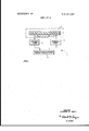
- FIG. 1 is a block diagram illustrating the process of the compacting system.
- FIG. 2 is a schematic diagram of one embodiment of encoding logic comprising part of the compacting system.
- FIG. 3 is a schematic diagram of one embodiment of decod ing logic comprising part of the compacting system.
- FIG. 1 illustrates a block diagram of the compacting system 1.
- Block 2 represents the 12 Binary Coded Decimal (8CD) bits of a three-digit decimal number.
- the 12 bits may be contained in an input storage register or by any means which processes a number for storage in a memory.
- the hundreds digit is represented by bit positions Il -H the tens digit by bit positions T T,; and the units digit by bit positions U,U,.
- the number of decimal digits may be increased by increasing the number of bits used to represent the number. For example, four additional bits could be added to represent the thousands digit of a decimal number.
- the number of bits and logic configuration of a decimal number depend on the numerical code being used.
- the decimal digits are represented by a Binary Coded Decimal code. It should be understood, however, that other codes are also within the scope of the invention.
- a Binary Coded Decimal code was selected for purposes of describing one embodiment of theinvention.
- FIG. 1 could be duplicated for parallel operation or used serially to encode and store a decoded number having any number ofdigits.
- the number could be processed in groups of three digits each.
- Block 3 in FIG. 1 represents the encoding logic and block 5 the decoding logic between the decimal number presented for storage and the storage locations for the encoded and stored bits.
- the encoded bits may be stored in storage locations of a memory, such as a plated wire memory, core memory, and other types of memories well known to persons skilled in the art.
- the storage area is represented by block 4.
- the encoding and decoding logic, blocks 3 and 5, are shown in more detail in FIGS. 2 and 3 respectively.
- the decimal number in block 2 is encoded by logic in block 3 for storage in storage locations in block 4.
- the stored bits in block 4 are decoded by logic in block 5 for reading out the decimal number into block 2.
- the decimal number is encoded so that it is not necessary to store bits representing each digit. Normally, as indicated by block 2, 12 bits are required to store three decimal digits represented by BCD code. However, as indicated in the FIG. .1, only [0 bits are required to store the three decimal digits. The reduction in storage space is made possible by utilizing certain storage bits to represent the position and value of the high-valued decimal digits. The remaining decimal digits are encoded and stored in octal form in the remaining bit positions of storage represented by block 4. The storage bit-locations are designated by M M,-M,.
- a similar compacting scheme can be used to encode and decode two decimal digits, normally requiring eight bits of storage, in seven bit codes storage. For a two-digit number,
- the first storage bit for example M is used to indicatethe high-valued bit.
- Storage bits M -M are also used.
- Storage bits M,,-M- may be eliminated for a two-digit system.
- An example of the utility of having both a three-digit scheme and a twodigit scheme in one system can be seen by considering an 1 1- digit number. Ordinarily, 44 storage bits are required to store an 1 l-digit decimal number. By using a three decimal digit and two decimal digit compacting scheme, only 37 bits of storage space are required. There is no advantage in providing a compacting storage scheme for one decimal digit.
- decimal digits 8 and 9 are described as being the highvalued, or large, decimal digits and decimal digits 0 through 7 are described as being the low-valued or small digits.
- the larger digits are represented by the logic state of certain of the storage bits while the least significant digits are stored in octal form in other storage locations.
- bit positions M,,-M are relatively small and are represented by the logic bits stored in bit positions M,,-M,.
- the numbers are encoded and stored in octal groups. If a logic one is stored in M and if M, and M, are not both ones, the bit' positions M, and M, indicate the relative position of a single large digit and M-, indicates whether the large digit is an 8 or a 9. Bit positions M through M, store the value of the two remaining small digits.
- bit positions M,,, M, and M are ones, the decimal number contains two large digits.
- the M, and M, bit positions indicate the relative position of the remaining small decimal digit which is stored in bit positions M, through M,.
- Bit positions M-, and M indicate the position and whether the large digits are 8 and/or 9.
- bit positions M-,, M, and M indicate the position of and whether the digits are 8 and/or 9.
- M,, M M represent hundreds decimal digit in octal.
- M,,, M M represent tens decimal digit in octal.
- M,,, M,, M represent units decimal digit in octal.
- M,,, M indicate position of a single 8 or 9 decimal digit.
- M,,', M indicate that the hundreds digit is an 8 or a 9.
- M,,, M,;' indicate that the units digit is an 8 or a 9.
- Mg M indicate that the tens digit is an 8 or a 9.
- M indicates that the digit is a 9.
- M,,, M M represent leading small decimal digit in octal.
- M,,, M,, M represent trailing small decimal digit in octal.
- M,,, M,, M represent the third decimal digit in octal.
- M and M indicate the relative values of the large digits in the corresponding positions.
- M M,, M indicate whether the digits in the corresponding positions are 8's or 9's.
- Xs represent unused bits for the particular digital number being encoded.
- the H, T and U letters indicate that octal groups representing the corresponding decimal digits are stored in the corresponding M, through M, bit positions.
- primes of the letters described herein e.g., H, T, U, and M, indicate that a logic 0 (false state) is represented by the primed letter.
- table 1 contains a numerical summary in the ,form of a truth table.
- M is also true to indicate that the large digit is a 9.
- the octal group M, through M then stores the digit and octal group, M, through M, stores the tens digit.
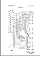
- FIG. 2 is a schematic diagram of one embodiment of encoding logic which can be used in implementing block 3 of FIG. 1.
- Signals representing the logic states of each of the BCD bits .H,-H,,,' T,, U,U,, representing the decimal number appear on terminals 30 through 41.
- the numbers are encoded in ac- ,cordance with tables I and II, described above, by the logic gates designated generally by number 42.
- the encoded values appear as outputs from NAND-gates 43 through 52.
- Outputs from the NAND gates provide signals on terminals 53 through 62.
- the signals are stored in bit positions M, through M,, as shown.
- a relatively low, for example electrical ground, signal level is stored as a logic zero and a relatively high, for example +25 volts, is stored as a logic one. Whether or not the relatively high voltage level is a or a is determined as a function of the particular types of devices being used and the logic convention adopted.
- inverters 63, 64, and 65 are utilized for inverting the inputs on terminals 34 and 38 respectively.
- Other inverters 66, and 67 are also included as part of the gates represented by numeral 42 in order td'implement the encoding logic.
- NAND-gates 68 through 101 are also required.
- the low signal on terminal 31 provides a low input to NAND-gate 69 which results in a high output. Since neither the tens or units digits are 8s or 9s, T, and U, are both low. Therefore, the output from NAND-gate 68 is high.
- the low signal on terminal 38 is inverted through inverter 65 and provides a third high input to NAND-gate 44. Since all the inputs are high, the output on terminal 54 for M is low, A similar analysis can be made for signals on terminals 55 and 56 representing bit positions M and M,, respectively.
- FIG. 2 encoder Logic for the FIG. 2 encoder is summarized below.
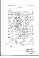
- FIG. 3 is a schematic diagram of one embodiment of decoding logic which may be used to implement the decoding portion of block 5 shown in FIG. 1.
- the FIG. 3 embodiment decodes signals representing logic one and logic zero states stored in bit positions M through M, for providing B CD bits number.
- the BCD bits corresponding to hit positions II,H,, T,T,,,' .,U, appear on terminals 102 through 113 for each of the Binary Coded Decimal bits, respectivelyJ-The storedlogic signals corresponding to bit positionsM, through M, appear from storage'on terminals 114 through 123.
- Logic gates necessary to decode the stored bits to representthe decimal number are designated generally by the number 124.
- OR-gates 125, 126, and 127 provide output signals representing H, through 11,, respectively.
- OR-gates 128, 129 and 130 provide output signals representing bit positions T through T',, respectively, CIR-gate 131 provides a signal representing the U bit.
- AND-gate 132 provides an output signal representing H, and AND-gate 133 provides output signal representing T,.
- AND-gates 134 and 135 provide signals representing U and U, bits, respectively.
- the M signal appearing on terminal 114 is inverted through inverter gate 136.
- signals appearing on terminals 115, 116 and 119 representing bit positions M,, M, and M,, respectively, are inverted through inverter gates 137, 138, and 139, respectively.
- Exclusive OR-gate provides 'the exclusive OR of M, and M,.
- the other gates of the decoder logic include AND-gate; 141, OR-gate 142, AND-gate 143, OR-gate 144, ANDgates, through 169, OR-gates through 179, inverters through 182, and AND-gates 183, 184.
- octal numbers representing the decimal digits 6 and 2 are stored in octal groups M, through M, and M, through M,, respectively.
- AND-gate 132 receives one true inputfrom terminal 114.
- the low signal on terminal 115 More invertedto provide a true signal to AND-gate 143.
- the low signal on terminal 116 is also inverted through gate 138 to provide a second true signal to AND-gate 143. Since both inputs to AND-gate 143 are true, it provides a true output to OR-gate 144.
- OR-gate 144 then provides a second true input to AND- gate 132 which provides a high output on terminal 102 representing H, The output on terminal 103 representing bit H is low or false since all the inputs to OR-gate 125 are false.
- OR-gate 125 the AND-gate 141 input to OR-gate 125 is false since AND-gate 141 receives a false input from inverter gate 136.
- the second input to OR-gate 125 is false since one input to AND-gate 146 is received from exclusive OR-gate 140, whose inputs M, and M,; are both false.
- the last input to OR-gate 125 is also false since AND-gate 157 receives an input from AND-gate 156 which receives an input from AND- gate 149 whose inputs M and M; from terminals 115 and 116 are both false. Therefore, the output from AND-gate 157 is false. Since all the inputs to OR-gate 125 are false, the output on terminal 103 representing H is also false. A similar explanation is true for the output terminal 104 from OR-gate 126.
- the output on terminal 105 representing H is a 1 since OR- gate 127 receives a true input from AND-gate 152.
- AND-gate 152 is true since it receives a true or high signal from terminal 117 representing M and a second true input from OR-gate 142.
- OR-gate 142 receives a true input signal from AND-gate 143.
- AND-gate 143 is true since the low signal on terminal 115 representing M, is inverted through gate 137 to provide one true input to AND-gate 143.
- the second true input to AND-gate 143 is received from inverter gate 138 which inverts the low input on terminal 116.
- a system for the compact storage of decimal numbers having a plurality of decimal digits comprising,
- a plurality of storage locations including a first plurality of storage locations responsive to said encoding logic for storing bits of logic information representing the value for position of any relatively high-valued decimal digits in said decimal number,
- said encoding logic converting each relatively low-valued decimal digit of said decimal number into a binary coded representation, relatively low-valued decimal digits include decimal digits other than a high-valued decimal digit, and
- said plurality of storage locations including a second plurality of storage locations responsive to said encoding logic for storing the binary coded representation for any relatively low-valued decimal digits in said decimal number.
- said encoding logic further includes means for dividing a decimal number comprising a plurality of digits into a plurality of groups of decimal digits, with each of said groups of decimal digits being encoded by said encoding logic in parallel for being stored in said plurality of storage locations.
- said encoding, logic further includes means for dividing a decimal number into a plurality of groups of decimal digits, and means for examining each ofsaid groups of decimal digits serially.
- decoding logic for examining the bits of logic information stored in said first plurality of storage locations for providing as an output from said system, decimal digits having a value and a position corresponding to the value and position of the relatively high-valued decimal digits in the decimal number examined by said encoding logic, and said decoding logic converting the binary coded representation of each relatively lowvalued decimal digit stored in second plurality of storage locations for providing as an output simultaneously with the output of said high-valued decimal digits, the low-valued decimal digits of the decimal number examined by said encoding logic.
- decimal number examined by said encoding logic is represented by a Binary Coded Decimal numerical code and wherein said encoding logic converts certain decimal digits of said Binary Coded Decimal number into an octal coded decimal number.
- said encoding logic includes logic gates for determining if all decimal digits of the decimal number examined by said encoding logic are in excess ofthe decimal digit 8, and
- said plurality of storage locations storing each of the decimal digits in excess of the decimal digit 8.
- said encoding logic includes logic gates for determining if the digits of a decimal number examined by said encoding logic contains a single 8 or 9 digit, said encoding logic providing an input to said first plurality of storage locations for storing a bit representing the value and the position of said single 8 or 9 di it, said encoding logic roviding inputs to said second plura ity of storage locations or storing t e decimal digits of said decimal number examined by said encoding logic in said second plurality of storage locations.
- said encoding logic includes logic gates for determining whether two digits of said decimal number are an 8 and/or a 9 digit and further includes logic gates for indicating the position of the relatively low-valued digits ofsaid decimal number as well as for indicating the value and position of said two digits, said two digits comprising the relatively high-valued decimal digits of said decimal number.
Landscapes
- Engineering & Computer Science (AREA)
- Theoretical Computer Science (AREA)
- Compression, Expansion, Code Conversion, And Decoders (AREA)
Abstract
The system includes encoding logic which examines each bit of a decimal number to determine the number and position of highvalued digits, eight or nine, in the decimal number. Certain storage bit positions are allocated to the high-valued digits. The high-valued digits are not encoded in the normal sense. The logic state of the certain storage bit positions indicate value and position of the high-valued digits in the decimal number. The remaining digits of the decimal number are encoded and stored in the remaining bit positions. Decoding logic examines the stored bits of information to provide as an output the decoded decimal number.
Description
United States Patent [72] inventor Theodore M. Hertz Whittier, Calif. [21] Appl.No. 885,l65 [22] Filed Dec. 15, I969 [45] Patented Nov. 2, 1971 [73] Assignee North American Rockwell Corporation [54] SYSTEM FOR THE COMPACT STORAGE 0 DECIMAL NUMBERS t 9 Claims, 3 Drawing Figs.
[52] US. Cl 340/1725, 235/l55, 340/347 DD [5l] Int. Cl G06! 5/02 [50] Field oiSearch 340/1725, 347 DD; 235/155 [56] References Cited UNITED STATES PATENTS 3,310,786 3/l967 Rinaldietal 340/1725 3,432,8ll 3/1969 Rinaldietal 340/l72.5
OTHER REFERENCES Primary Examiner-Raulfe B. Zache Assistant Examiner-Melvin B. Chapnick Attorneys-L. Lee Humphries, H. Fredrick Hamann and Robert G. Rogers ABSTRACT: The system includes encoding logic which examines each bit ofa decimal number to determine the number and position of high-valued digits, eight or nine, in the decimal number. Certain storage bit positions are allocated to the high-valued digits. The high-valued digits are not encoded in the normal sense. The logic state of the certain storage bit positions indicate value and position of the high-valued digits in the decimal number. The remaining digits of the decimal number are encoded and stored in the remaining bit positions. Decoding logic examines the stored bits ofinformation to provide as an output the decoded decimal number,
u u u u ENCODING,
LOGIC 3 F5 DECODIN G/ LOGIC PATENTEUunvz 1am 3618047 SHEET 2 [1F 3 I I 4 l INVIi'N'H )K. nsooone M. HERTZ FIG. 2
ATTORNEY PATENTEUrmvz |97| 3.618.047
SHEET 3 UF 3 I'N VIZN'IYJR.
THEODORE M. HERTZ BYWDW ATTORNEY BACKGROUND OF THE INVENTION 1. Field of the Invention The invention relates to a system forlcompact storage of decimal numbers and more particularly to a system in which certain bits of information are stored to indicate the value and position of certain digits of the numbers.
2. Description of Prior Art Storage of decimal numbers by certain systems normally requires four hits of storage space per decimal digit. It would be preferred if the storage requirements for a decimal number could be reduced. In that way, the usable capacity of a memory could be increased without increasing the actual storage area. However, the increased advantages would be slight if slow and/or complex arithmetic conversions were required as part of the reduction process.
Therefore, a system is preferred which can encode a decimal number to reduce the storage space normally required to store the number. The preferred system would also require a decoder for generating the decimal number from the stored bits. The encoding and decoding logic for compacting the storage should be relatively fast without requiring a complex arithmetic conversion. The present invention provides the preferred capability required for a compact storage system.
SUMMARY OF THE INVENTION Briefly, the system for compacting the storage of decimal numbers includes logic for encoding a decimal number so that the storage of each bit of the decimal number is not required. Certain encoded bits indicate the position and value of certain valued digits of the decimal number, e.g., an 8 or a 9. The encoded bits, less in number than the bits required to represent a decimal number, are stored. Decoding logic receives the stored encoded bits from storage and produces as an output the decimal number represented by the stored bits.
In a preferred system, 12 Binary Coded Decimal (BCD) bits of three decimal digits, each digit comprising four of the bits, can be encoded and stored in bits of storage area. The lowvalued digits, 0-7, are stored in actual groups while the highvalued digits are represented by other stored bits.
Decimal numbers of other digits may be encoded in a manner similar to the encoding of a decimal number having three digits. For example, bits are required to encode a decimal number having six digits.
In addition, although the preferred embodiment is described for BCD, the system may be used for compacting numbers represented by any decimal code. For example, the system can be used to compact numbersrepresented by an excess 3 code. The separation of the digits by value may be changed as a function ofthe decimal code used.
The system is useful in computers, data processors, etc., involving storage of numerical data in a decimal form. It is also useful for read-only memory systems which store tables of values for trigonometric functions, logarithms, etc. In such systems, only decoding is required.
Therefore, it is an object of this invention to provide a system for compacting the storage of decimal numbers.
It is another object of this invention to provide a process for compacting the storage of decimal numbers.
A further object of this invention is to provide a system for encoding bits representing a decimal number so that a reduced number of bits of storage space is required for the decimal number.
A still further object of the invention is to provide a compact storage system in which certain stored bits indicate the value and position of the high-valued digits of a decimal number and other stored bits represent the remaining digits of the decimal number.
Another object of this invention is to provide a compact storage system which can be used to reduce the number of bits required for storing decimal numbers represented by any decimal code.
A still further object of the invention is to provide a simple encoding and decoding scheme which permits storage of groups of three decimal digits by using the same logic for either the serial or parallel encoding and decoding of the three decimal digits.
A further object of the: invention is to provide a compactstorage scheme that does not require relatively slow and/or complex arithmetic conversions.
These and other objects of the invention will become more apparent when taken in connection with the drawings, a brief description of which follows:
BRIEF DESCRIPTION OF DRAWINGS FIG. 1 is a block diagram illustrating the process of the compacting system.
FIG. 2 is a schematic diagram of one embodiment of encoding logic comprising part of the compacting system.
FIG. 3 is a schematic diagram of one embodiment of decod ing logic comprising part of the compacting system.
DESCRIPTION OF PREFERREDEMBODIMENT FIG. 1 illustrates a block diagram of the compacting system 1. Block 2 represents the 12 Binary Coded Decimal (8CD) bits of a three-digit decimal number. The 12 bits may be contained in an input storage register or by any means which processes a number for storage in a memory. The hundreds digit is represented by bit positions Il -H the tens digit by bit positions T T,; and the units digit by bit positions U,U,.
The number of decimal digits may be increased by increasing the number of bits used to represent the number. For example, four additional bits could be added to represent the thousands digit of a decimal number. The number of bits and logic configuration of a decimal number depend on the numerical code being used. In the FIG. I embodiment, the decimal digits are represented by a Binary Coded Decimal code. It should be understood, however, that other codes are also within the scope of the invention. A Binary Coded Decimal code was selected for purposes of describing one embodiment of theinvention.
It is also pointed out that the logic of FIG. 1 could be duplicated for parallel operation or used serially to encode and store a decoded number having any number ofdigits. The number could be processed in groups of three digits each.
The encoding and decoding logic, blocks 3 and 5, are shown in more detail in FIGS. 2 and 3 respectively. The decimal number in block 2 is encoded by logic in block 3 for storage in storage locations in block 4. The stored bits in block 4 are decoded by logic in block 5 for reading out the decimal number into block 2.
The decimal number is encoded so that it is not necessary to store bits representing each digit. Normally, as indicated by block 2, 12 bits are required to store three decimal digits represented by BCD code. However, as indicated in the FIG. .1, only [0 bits are required to store the three decimal digits. The reduction in storage space is made possible by utilizing certain storage bits to represent the position and value of the high-valued decimal digits. The remaining decimal digits are encoded and stored in octal form in the remaining bit positions of storage represented by block 4. The storage bit-locations are designated by M M,-M,.
A similar compacting scheme can be used to encode and decode two decimal digits, normally requiring eight bits of storage, in seven bit codes storage. For a two-digit number,
the first storage bit, for example M is used to indicatethe high-valued bit. Storage bits M -M, are also used. Storage bits M,,-M-, may be eliminated for a two-digit system. An example of the utility of having both a three-digit scheme and a twodigit scheme in one system can be seen by considering an 1 1- digit number. Ordinarily, 44 storage bits are required to store an 1 l-digit decimal number. By using a three decimal digit and two decimal digit compacting scheme, only 37 bits of storage space are required. There is no advantage in providing a compacting storage scheme for one decimal digit.
In the description of the preferred embodiment of the invention, decimal digits 8 and 9 are described as being the highvalued, or large, decimal digits and decimal digits 0 through 7 are described as being the low-valued or small digits. The larger digits are represented by the logic state of certain of the storage bits while the least significant digits are stored in octal form in other storage locations.
If a logic zero is stored in M all the decimal digits are relatively small and are represented by the logic bits stored in bit positions M,,-M,. The numbers are encoded and stored in octal groups. If a logic one is stored in M and if M, and M, are not both ones, the bit' positions M, and M, indicate the relative position of a single large digit and M-, indicates whether the large digit is an 8 or a 9. Bit positions M through M, store the value of the two remaining small digits.
[f bit positions M,,, M, and M; are ones, the decimal number contains two large digits. The M, and M, bit positions indicate the relative position of the remaining small decimal digit which is stored in bit positions M, through M,. Bit positions M-, and M, indicate the position and whether the large digits are 8 and/or 9.
If M,,, M,, M M, and M, are ones, all three decimal digits are large numbers. In that case, bit positions M-,, M, and M, indicate the position of and whether the digits are 8 and/or 9.
A summary of the encoding process is contained in table I as pllw z.
TABLE II M,,, M M represent hundreds decimal digit in octal. M,,, M M, represent tens decimal digit in octal. M,,, M,, M represent units decimal digit in octal.
M,,, M indicate position of a single 8 or 9 decimal digit. M,,', M, indicate that the hundreds digit is an 8 or a 9. M,,, M,;' indicate that the units digit is an 8 or a 9.
Mg M, indicate that the tens digit is an 8 or a 9.
M, indicates that the digit is an 8.
M indicates that the digit is a 9.
M,,, M M, represent leading small decimal digit in octal. M,,, M,,, M, represent trailing small decimal digit in octal.
two digits are an 8 or a 9.
M,,, M, indicate the position of the third digit.
M,,, M,, M, represent the third decimal digit in octal.
M and M, indicate the relative values of the large digits in the corresponding positions. M
M,,=M,=M,;=M;=M,=l
All three digits are 8 or 9.
M M,, M, indicate whether the digits in the corresponding positions are 8's or 9's.
The above tables can be used to describe a specific example wherein a decimal number is encoded and stored in memory. For purposes of the illustration, suppose the decimal number 962 is processed into an input register for encoding and storage. Since the decimal number contains a relatively large digit, 9, then M,,=l. M =l indicates that the large digit is a 9.
TABLE I M0 Ma e r s M, M; M2 M1 Explanation 0 H H1 H; T; T T1 U U; U, All decimal digits less than 8v 1 0 0 0 T3 T2 T1 U3 U3 U1 Hundreds digit=8. 1 0 0 1 T '1; T1 U; U U1 Hundred's digit=9. 1 0 1 0 H3 H9 H1 U3 U2 U1 TGH'S dlgit=8. 1 0 1 1 H; H2 H1 U U U1 Ten's digit= 9. 1 1 0 0 H H1 H, T3 T T1 Unit's diglt=8. 1 1 0 1 H; H, H, T T, T1 Units digit=9. 1 1 1 0 0 0 0 H, H, H] Tens and units digits=8. 1 1 1 1 0 0 0 H; H; H1 Ten's=9, unlts=8. 1 1 1 0 0 0 1 H H3 H1 Tens==8, unlts=9. 1 1 1 1 0 0 1 H; H: H1 Tens and units 9. 1 1 1 0 0 1 0 T3 T1 T1 Hundreds and units=8. 1 1 1 1 0 1 0 Ta '1; T1 Hundreds=9, unlt's=8. 1 1 1 0 0 1 1 T; T T1 Hundreds=8, units=9. 1 1 1 1 0 1 1 T3 T1 T1 Hundreds and unit's =9. l 1 1 0 1 0 0 U, U, U Hundreds and tens=8. 1 1 1 1 1 0 0 U U, U1 Hundreds=9, tens=8. 1 1 1 0 1 0 1 U3 U2 U1 Hundred's=8, tens=9. 1 1 1 1 1 D 1 U U U Hundreds and ten's=9. 1 1 1 0 1 1 0 X X 0 All dlgits=8. 1 1 1 0 1 1 0 X X 1 l1=8, t=,-S, u=9. 1 1 1 0 1 1 1 X X 0 l1=8,t=9, u=8. 1 1 1 0 1 1 1 X X 1 h=8, t ,=u=9. 1 1 1 1 1 1 0 X X 0 h 9, tr,=u= 8. 1 1 1 1 1 1 0 X X 1 h=9, t-S, u-Q. 1 1 1 1 1 1 1 X X 0 h=9, t==9, u=8. 1 1 1 1 l 1 1 X X 1 All digits= 9.
Xs represent unused bits for the particular digital number being encoded. The H, T and U letters indicate that octal groups representing the corresponding decimal digits are stored in the corresponding M, through M, bit positions. The
primes of the letters described herein, e.g., H, T, U, and M, indicate that a logic 0 (false state) is represented by the primed letter.
The following table is a written summary of the encoding process, whereas table 1 contains a numerical summary in the ,form of a truth table.
processed into an input register for encoding and storage. For
that case, M,,=l to indicate the presence of a single large digit. M, is also true to indicate that the large digit is a 9. M,,=l, and .M,,=O to indicate that the units digit is a 9. The octal group M, through M, then stores the digit and octal group, M, through M, stores the tens digit.
If the tens digit had been a 9, for example, M,,=O, M =l and Mal, the hundreds and units digits are stored in the octal groups M through M, and M, through M,, respectively.
FIG. 2 is a schematic diagram of one embodiment of encoding logic which can be used in implementing block 3 of FIG. 1.]
Signals representing the logic states of each of the BCD bits .H,-H,,,' T,, U,U,, representing the decimal number appear on terminals 30 through 41. The numbers are encoded in ac- ,cordance with tables I and II, described above, by the logic gates designated generally by number 42. The encoded values appear as outputs from NAND-gates 43 through 52. Outputs from the NAND gates provide signals on terminals 53 through 62. The signals are stored in bit positions M, through M,, as shown. A relatively low, for example electrical ground, signal level is stored as a logic zero and a relatively high, for example +25 volts, is stored as a logic one. Whether or not the relatively high voltage level is a or a is determined as a function of the particular types of devices being used and the logic convention adopted.
In order to provide primes certain of the Binary Coded Decimal inputs (11,, T,,, and U inverters 63, 64, and 65 are utilized for inverting the inputs on terminals 34 and 38 respectively. Other inverters 66, and 67 are also included as part of the gates represented by numeral 42 in order td'implement the encoding logic. NAND-gates 68 through 101 are also required.
Since the encoding process was described in connection with tables I and II, it is not believed necessary to describe the encoding logic shown in FIG. 2 in great detail. However, as a egre ate, the previousl encoded and sidi i dEciifii simple illustration, assume that the hundredths digitof the decimal number is an 8 and the remaining digits are small. In that case, H,=l and H, through H,=0s. It is known from the above description that M, should equal 1, and that M, through M, should equal Os. Therefore, the output from NAND-gate 43 should be high and the outputs from NAND-gates 44 through 46 should be low. Outputs from the other NAND- gates 47 through 52, correspond to the octal values represented by the bits T -T, and U, of the remaining small digits.
The high signal on terminal 30 is inverted through gate 63 and appears as a low input to AND-gate 43. Any low input to a NAND-gate results in a high output. Therefore, a M =l as indicated above. The low signal on terminal 31 provides a low input to NAND-gate 69 which results in a high output. Since neither the tens or units digits are 8s or 9s, T, and U, are both low. Therefore, the output from NAND-gate 68 is high. In addition, the low signal on terminal 38 is inverted through inverter 65 and provides a third high input to NAND-gate 44. Since all the inputs are high, the output on terminal 54 for M is low, A similar analysis can be made for signals on terminals 55 and 56 representing bit positions M and M,, respectively.
Logic for the FIG. 2 encoder is summarized below.
FIG. 3 is a schematic diagram of one embodiment of decoding logic which may be used to implement the decoding portion of block 5 shown in FIG. 1. The FIG. 3 embodiment decodes signals representing logic one and logic zero states stored in bit positions M through M, for providing B CD bits number. The BCD bits corresponding to hit positions II,H,, T,T,,,' .,U,, appear on terminals 102 through 113 for each of the Binary Coded Decimal bits, respectivelyJ-The storedlogic signals corresponding to bit positionsM, through M, appear from storage'on terminals 114 through 123. Logic gates necessary to decode the stored bits to representthe decimal number are designated generally by the number 124.
OR- gates 125, 126, and 127 provide output signals representing H, through 11,, respectively. OR- gates 128, 129 and 130 provide output signals representing bit positions T through T',, respectively, CIR-gate 131 provides a signal representing the U bit. AND-gate 132 provides an output signal representing H, and AND-gate 133 provides output signal representing T,. AND- gates 134 and 135 provide signals representing U and U, bits, respectively.
The M signal appearing on terminal 114 is inverted through inverter gate 136. Similarly, signals appearing on terminals 115, 116 and 119 representing bit positions M,, M, and M,, respectively, are inverted through inverter gates 137, 138, and 139, respectively.
Exclusive OR-gate provides 'the exclusive OR of M, and M,. The other gates of the decoder logic include AND-gate; 141, OR-gate 142, AND-gate 143, OR-gate 144, ANDgates, through 169, OR-gates through 179, inverters through 182, and AND- gates 183, 184.
The above logic equations have beensirnplified somewhat by the P, through P, logic terms, the X, logic term, I,, I, and I, terms, and the S, through S, terms. The logic equations represented by the terms may be substituted for the terms in the other equations, if desired. For convenience, the Binary Coded Decimal terms were written in the condensed manner indicated.
By way of describing a specific example, assume that the decimal number 962 was stored in bit positions M, through M,. Therefore, I-I, should equal 1, H,=0, H,=O, and H,=l. In addition, T,=0, T =l, T,=l, and T,=0; U,=0, U,=0, U,=, and U,=G.
Since the most significant digit is a 9 and is the hundreds digit, M =l M =0, M,,=0, and Ma]. No attempt will be made to decode the remaining numbers. As indicated previously, octal numbers representing the decimal digits 6 and 2 are stored in octal groups M, through M, and M, through M,, respectively.
Since M is a l, AND-gate 132 receives one true inputfrom terminal 114. The low signal on terminal 115 More invertedto provide a true signal to AND-gate 143.The low signal on terminal 116 is also inverted through gate 138 to provide a second true signal to AND-gate 143. Since both inputs to AND-gate 143 are true, it provides a true output to OR-gate 144. OR-gate 144 then provides a second true input to AND- gate 132 which provides a high output on terminal 102 representing H, The output on terminal 103 representing bit H is low or false since all the inputs to OR-gate 125 are false. More specifically, the AND-gate 141 input to OR-gate 125 is false since AND-gate 141 receives a false input from inverter gate 136. The second input to OR-gate 125 is false since one input to AND-gate 146 is received from exclusive OR-gate 140, whose inputs M, and M,; are both false. The last input to OR-gate 125 is also false since AND-gate 157 receives an input from AND-gate 156 which receives an input from AND- gate 149 whose inputs M and M; from terminals 115 and 116 are both false. Therefore, the output from AND-gate 157 is false. Since all the inputs to OR-gate 125 are false, the output on terminal 103 representing H is also false. A similar explanation is true for the output terminal 104 from OR-gate 126.
The output on terminal 105 representing H is a 1 since OR- gate 127 receives a true input from AND-gate 152. AND-gate 152 is true since it receives a true or high signal from terminal 117 representing M and a second true input from OR-gate 142. OR-gate 142 receives a true input signal from AND-gate 143. AND-gate 143 is true since the low signal on terminal 115 representing M, is inverted through gate 137 to provide one true input to AND-gate 143. The second true input to AND-gate 143 is received from inverter gate 138 which inverts the low input on terminal 116.
It "should be understood that addiiBHal 'eaisamfirar other numbering systems could also be provided in a manner,
similar to the FIGS. 2 and 3. In addition, the encoding and decoding logic would be written and implemented for decimal numbers having other than three digits. Provisions could be made for whole and fractional decimal numbers as well as for the sign of the decimal numbers. It is believed that such modifications are within the abilities of a person skilled in the art, and for that reason such additional embodiments are not described in detail herein.
1 claim:
1. A system for the compact storage of decimal numbers having a plurality of decimal digits, said system comprising,
encoding logic for examining each decimal digit of a decimal number to determine the value of each relatively high-valued decimal digit and the position of each relatively high-valued decimal digit in the decimal number relative to each other decimal digit, relatively high-valued decimal digits including decimal digits 8, 9, and combinations thereof,
a plurality of storage locations, including a first plurality of storage locations responsive to said encoding logic for storing bits of logic information representing the value for position of any relatively high-valued decimal digits in said decimal number,
said encoding logic converting each relatively low-valued decimal digit of said decimal number into a binary coded representation, relatively low-valued decimal digits include decimal digits other than a high-valued decimal digit, and
said plurality of storage locations including a second plurality of storage locations responsive to said encoding logic for storing the binary coded representation for any relatively low-valued decimal digits in said decimal number.
2. The system as recited in claim 1 wherein said encoding logic further includes means for dividing a decimal number comprising a plurality of digits into a plurality of groups of decimal digits, with each of said groups of decimal digits being encoded by said encoding logic in parallel for being stored in said plurality of storage locations.
3. The system as recited in claim 1 wherein said encoding, logic further includes means for dividing a decimal number into a plurality of groups of decimal digits, and means for examining each ofsaid groups of decimal digits serially.
4. The system as recited in claim 1 further comprising decoding logic for examining the bits of logic information stored in said first plurality of storage locations for providing as an output from said system, decimal digits having a value and a position corresponding to the value and position of the relatively high-valued decimal digits in the decimal number examined by said encoding logic, and said decoding logic converting the binary coded representation of each relatively lowvalued decimal digit stored in second plurality of storage locations for providing as an output simultaneously with the output of said high-valued decimal digits, the low-valued decimal digits of the decimal number examined by said encoding logic.
5. The system as recited in claim 1 wherein the decimal number examined by said encoding logic is represented by a Binary Coded Decimal numerical code and wherein said encoding logic converts certain decimal digits of said Binary Coded Decimal number into an octal coded decimal number.
6. The system as recited in claim 1 wherein said encoding logic includes logic gates for determining if all decimal digits of the decimal number examined by said encoding logic are in excess ofthe decimal digit 8, and
said plurality of storage locations storing each of the decimal digits in excess of the decimal digit 8.
7. The system as recited in claim 1 wherein said encoding logic includes logic gates for determining if the digits of a decimal number examined by said encoding logic contains a single 8 or 9 digit, said encoding logic providing an input to said first plurality of storage locations for storing a bit representing the value and the position of said single 8 or 9 di it, said encoding logic roviding inputs to said second plura ity of storage locations or storing t e decimal digits of said decimal number examined by said encoding logic in said second plurality of storage locations.
8. The system as recited in claim 1 wherein said encoding logic includes logic gates for determining whether two digits of said decimal number are an 8 and/or a 9 digit and further includes logic gates for indicating the position of the relatively low-valued digits ofsaid decimal number as well as for indicating the value and position of said two digits, said two digits comprising the relatively high-valued decimal digits of said decimal number.
Claims (9)
1. A system for the compact storage of decimal numbers having a plurality of decimal digits, said system comprising, encoding logic for examining each decimal digit of a decimal number to determine the value of each relatively high-valued decimal digit and the position of each relatively high-valued decimal digit in the decimal number relative to each other decimal digit, relatively high-valued decimal digits including decimal digits 8, 9, and combinations thereof, a plurality of storage locations, including a first plurality of storage locations responsive to said encoding logic for storing bits of logic information representing the value for position of any relatively high-valued decimal digits in said decimal number, said encoding logic converting each relatively low-valued decimal digit of said decimal number into a binary coded representation, relatively low-valued decimal digits include decimal digits other than a high-valued decimal digit, and said plurality of storage locations including a second plurality of storage locations responsive to said encoding logic for storing the binary coded representation for any relatively lowvalued decimal digits in said decimal number.
2. The system as recited in claim 1 wherein said encoding logic further includes means for dividing a decimal number comprising a plurality of digits into a plurality of groups of decimal digits, with each of said groups of decimal digits being encoded by said encoding logic in parallel for being stored in said plurality of storage locations.
3. The system as recited in claim 1 wherein said encoding logic further includes means for dividing a decimal number into a plurality of groups of decimal digits, and means for examining each of said groups of decimal digits serially.
4. The system as recited in claim 1 further comprising decoding logic for examining the bits of logic information stored in said first plurality of storage locations for providing as an output from said system, decimal digits having a value and a position corresponding to the value and position of the relatively high-valued decimal digits in the decimal number examined by said encoding logic, and said decoding logic converting the binary coded representation of each relatively low-valued decimal digit stored in second plurality of storage locations for providing as an output simultaneously with the output of said high-valued decimal digits, the low-valued decimal digits of the decimal number examined by said encoding logic.
5. The system as recited in claim 1 wherein the decimal number examined by said encoding logic is represented by a Binary Coded Decimal numerical code and wherein said encoding logic converts certain decimal digits of said Binary Coded Decimal number into an octal coded decimal number.
6. The system as recited in claim 1 wherein said encoding logic includes logic gates for determining if all decimal digits of the decimal number examined by said encoding logic are in excess of the decimal digit 8, and said plurality of storage locations storing each of the decimal digits in excess of the decimal digit 8.
7. The system as recited in claim 1 wherein said encoding logic includes logic gates for determining if the digits of a decimal number examined by said encoding logic contains a single 8 or 9 digit, said encoding logic providing an input to said first plurality of storage locations for storing a bit representing the value and the position of said single 8 or 9 digit, said encoding logic providing inputs to said second plurality of storage locations for storing the decimal digits of said decimal number examined by said encoding logic in said second plurality of storage locations.
8. The system as recited in claim 1 wherein said encoding logic includes logic gates for determining whether two digits of said decimal number are an 8 and/or a 9 digit and further includes logic gates for indicating the position of the relatively low-valued digits of said decimal number as well as for indicating the value and position of said two digits, said two digits comprising the relatively high-valued decimal digits of said decimal number.
9. The system as recited in claim 1 wherein said encoding logic includes logic gates for indicating whether all the digits of said decimal number are an 8 and/or a 9 digit and for indicating the value and position of each of 8 and/or 9 digits.
Applications Claiming Priority (1)
| Application Number | Priority Date | Filing Date | Title |
|---|---|---|---|
| US88516569A | 1969-12-15 | 1969-12-15 |
Publications (1)
| Publication Number | Publication Date |
|---|---|
| US3618047A true US3618047A (en) | 1971-11-02 |
Family
ID=25386303
Family Applications (1)
| Application Number | Title | Priority Date | Filing Date |
|---|---|---|---|
| US885165A Expired - Lifetime US3618047A (en) | 1969-12-15 | 1969-12-15 | System for the compact storage of decimal numbers |
Country Status (1)
| Country | Link |
|---|---|
| US (1) | US3618047A (en) |
Cited By (7)
| Publication number | Priority date | Publication date | Assignee | Title |
|---|---|---|---|---|
| US3689698A (en) * | 1971-04-07 | 1972-09-05 | Textron Inc | Multiplexing system |
| US3842414A (en) * | 1973-06-18 | 1974-10-15 | Ibm | Binary coded decimal conversion apparatus |
| US4032913A (en) * | 1973-04-09 | 1977-06-28 | Hitachi, Ltd. | Coding equipment providing compressed code |
| US4087811A (en) * | 1976-02-25 | 1978-05-02 | International Business Machines Corporation | Threshold decoder |
| US4334213A (en) * | 1980-02-04 | 1982-06-08 | Burroughs Corporation | Circuit for addressing binarily addressable memories with BCD addresses |
| US4626829A (en) * | 1985-08-19 | 1986-12-02 | Intelligent Storage Inc. | Data compression using run length encoding and statistical encoding |
| EP1231716A3 (en) * | 2001-01-27 | 2004-01-14 | International Business Machines Corporation | Decimal to binary coder/decoder |
Citations (1)
| Publication number | Priority date | Publication date | Assignee | Title |
|---|---|---|---|---|
| US3310786A (en) * | 1964-06-30 | 1967-03-21 | Ibm | Data compression/expansion and compressed data processing |
-
1969
- 1969-12-15 US US885165A patent/US3618047A/en not_active Expired - Lifetime
Patent Citations (2)
| Publication number | Priority date | Publication date | Assignee | Title |
|---|---|---|---|---|
| US3310786A (en) * | 1964-06-30 | 1967-03-21 | Ibm | Data compression/expansion and compressed data processing |
| US3432811A (en) * | 1964-06-30 | 1969-03-11 | Ibm | Data compression/expansion and compressed data processing |
Non-Patent Citations (3)
| Title |
|---|
| Bender, R. R. and Galage, D. J.; Packing Mode Control In IBM Technical Disclosure Bulletin; Vol. 4, No. 3, August, 1961; pp. 61 63; 340/172.5. * |
| Lengyel, E. J. and McMahon, R. F.; Direct Decimal to Binary Address Generator For Small Memories In IBM Technical Disclosure Bulletin; Vol. 9, No. 10, March, 1967; p. 1347; 340/347 * |
| Tilem, J. Y: Data Packing and Unpacking Means In IBM Technical Disclosure Bulletin; Vol. 5, No. 7, December, 1962; pp. 48 49; 340/172.5 * |
Cited By (7)
| Publication number | Priority date | Publication date | Assignee | Title |
|---|---|---|---|---|
| US3689698A (en) * | 1971-04-07 | 1972-09-05 | Textron Inc | Multiplexing system |
| US4032913A (en) * | 1973-04-09 | 1977-06-28 | Hitachi, Ltd. | Coding equipment providing compressed code |
| US3842414A (en) * | 1973-06-18 | 1974-10-15 | Ibm | Binary coded decimal conversion apparatus |
| US4087811A (en) * | 1976-02-25 | 1978-05-02 | International Business Machines Corporation | Threshold decoder |
| US4334213A (en) * | 1980-02-04 | 1982-06-08 | Burroughs Corporation | Circuit for addressing binarily addressable memories with BCD addresses |
| US4626829A (en) * | 1985-08-19 | 1986-12-02 | Intelligent Storage Inc. | Data compression using run length encoding and statistical encoding |
| EP1231716A3 (en) * | 2001-01-27 | 2004-01-14 | International Business Machines Corporation | Decimal to binary coder/decoder |
Similar Documents
| Publication | Publication Date | Title |
|---|---|---|
| US6525679B1 (en) | Binary to decimal coder/decoder | |
| GB1315060A (en) | Data processor | |
| US3581066A (en) | Programmable counting circuit | |
| US3618047A (en) | System for the compact storage of decimal numbers | |
| GB1070427A (en) | Data processing system | |
| GB1372907A (en) | Digital data transfer systems | |
| US3976980A (en) | Data reordering system | |
| US3753238A (en) | Distributed logic memory cell with source and result buses | |
| Brualdi et al. | Orphans of the first order Reed-Muller codes | |
| US3882483A (en) | Code converter system and method | |
| US3577142A (en) | Code translation system | |
| GB990557A (en) | Electronic adding system | |
| US3381117A (en) | Minimal pin multipurpose logic circuits | |
| US3229078A (en) | Code converter | |
| GB1187622A (en) | Improvements in or relating to apparatus for Generating Position-Control Signals | |
| US3749899A (en) | Binary/bcd arithmetic logic unit | |
| US4364025A (en) | Format switch | |
| US3526759A (en) | Parallel binary to parallel binary coded decimal converter | |
| US3842414A (en) | Binary coded decimal conversion apparatus | |
| US5285185A (en) | Dual-coded data comparator | |
| US3582944A (en) | Indicating system of 4-bit coded signal | |
| GB1567831A (en) | Binary data handing apparatus | |
| US3463910A (en) | Digit processing unit | |
| US3346730A (en) | Signed ternary carry generator using threshold logic elements | |
| SU840886A1 (en) | Device for comparing two n-digit numbers |