US3558982A - Current limiting protective means - Google Patents
Current limiting protective means Download PDFInfo
- Publication number
- US3558982A US3558982A US733150A US3558982DA US3558982A US 3558982 A US3558982 A US 3558982A US 733150 A US733150 A US 733150A US 3558982D A US3558982D A US 3558982DA US 3558982 A US3558982 A US 3558982A
- Authority
- US
- United States
- Prior art keywords
- switching means
- current
- state
- main circuit
- impedance
- Prior art date
- Legal status (The legal status is an assumption and is not a legal conclusion. Google has not performed a legal analysis and makes no representation as to the accuracy of the status listed.)
- Expired - Lifetime
Links
- 230000001681 protective effect Effects 0.000 title claims description 22
- 230000000670 limiting effect Effects 0.000 title claims description 10
- 230000004044 response Effects 0.000 claims description 29
- 238000010304 firing Methods 0.000 claims description 19
- 230000001960 triggered effect Effects 0.000 claims description 13
- 238000010791 quenching Methods 0.000 claims description 10
- 230000000171 quenching effect Effects 0.000 claims description 9
- 230000002159 abnormal effect Effects 0.000 claims description 6
- 230000003213 activating effect Effects 0.000 claims description 5
- 230000008859 change Effects 0.000 claims description 5
- 230000003111 delayed effect Effects 0.000 claims description 4
- 230000002457 bidirectional effect Effects 0.000 claims 1
- 230000003068 static effect Effects 0.000 abstract description 3
- 239000003990 capacitor Substances 0.000 description 7
- 230000009471 action Effects 0.000 description 3
- 238000010586 diagram Methods 0.000 description 3
- 230000004048 modification Effects 0.000 description 2
- 238000012986 modification Methods 0.000 description 2
- 239000004065 semiconductor Substances 0.000 description 2
- 230000001052 transient effect Effects 0.000 description 2
- 101100400378 Mus musculus Marveld2 gene Proteins 0.000 description 1
- 241000863814 Thyris Species 0.000 description 1
- 238000007664 blowing Methods 0.000 description 1
- 230000005611 electricity Effects 0.000 description 1
- 230000002401 inhibitory effect Effects 0.000 description 1
- 238000009434 installation Methods 0.000 description 1
- 230000007257 malfunction Effects 0.000 description 1
Images

Classifications
-
- H—ELECTRICITY
- H02—GENERATION; CONVERSION OR DISTRIBUTION OF ELECTRIC POWER
- H02H—EMERGENCY PROTECTIVE CIRCUIT ARRANGEMENTS
- H02H3/00—Emergency protective circuit arrangements for automatic disconnection directly responsive to an undesired change from normal electric working condition with or without subsequent reconnection ; integrated protection
- H02H3/02—Details
- H02H3/025—Disconnection after limiting, e.g. when limiting is not sufficient or for facilitating disconnection
Definitions
- a high-speed AC electric power switch and current-limiting impedance combination suitable for interconnecting a static inverter and its load circuit is arranged to respond to an overload condition by inserting the impedance in series with the load so fast that the inverter can remain in service with its integrity unimpaired.
- the switch is also arranged to subsequently isolate the load circuit from the inverter in the event that the overload condition has not otherwise been relieved within a predetermined length of time.
- feeders include suitable protective devices (e.g.,'fuses) for'au tomatically isolating an individual feedercircuit in the event of a fault involving solely that branch of the system.
- protective devices e.g.,'fuses
- my general objective is to provide improved protective means for accomplishing these ends.
- the switch illustrated in FIG. I is adapted to'be serially connected in a load current conducting path 41 between an electric power source and a load circuit.
- a total of three duplicate switches would be used in practice, all three sharing common controls 80.
- the load circuit typically comprises a bus having a plurality of separately protected feeder circuits or branches (not shown).
- the source could be a power distribution bus; and the load circuit a feeder individually protected bymy switch.
- the switch is useful'in a variety of settings, and it is particularlyadvantageous in an uninterruptible power system such as the one referred to briefly in the introduction of this specification and'explained more fully in copending U.S. application Ser. No. 733,446 filed on May 3 l, 1968, U.S.
- a main circuit 50 comprising load current conducting solid-state-controlled switching means
- the'main circuit is shunted by a subsidiary circuit 60 comprising'the combination of another switching means in series with current limiting impedance means 61.
- the solid-state-controlled'switchingm'eans of the main circuit 50 is normally maintained in a' relatively low resistance, turned-on state, whereby load current 'can easily traverse the switch.
- this switching means comprises first and second semiconductor controlled rectifie rs 51v and 52 disposed in inverse parallel relationship with one another as shown.
- Such devices are known generally asthyristors, and more information about them can be obtained from published literature such as the reference book SEMICONDUCTOR CON- TROLLED RECTIFIERS by F.
- Commutating means is providedfor high-speed turnoff of the first pair of thyristors when a slight oyerload is detected, whereupon through currentis forced to traverse the currentlimiting resistor whi ch limits its .rnagnitude while preserving service continuity.
- duplicate devices can be connected in parallel and series and operated in unison with the thyristors 51 and 51, respectively.
- the main thyristors are selected to safely conduct their respective shares of full load current continuously.
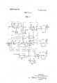
- FIG. 1 is a schematic diagram of a single-phase version of my improved protective means.
- FIG. 2 is a functional block diagram of apreferred embodiment of the controls shown as a single bl'oclt in FIG. 1.
- F IG. 1 the power circuit of the protective means has been shown inside a broken-line box labeled switch," and the associated controls are shown generally asa block 80. Further details ofthe controls are illustrated in FIG. 2 which ,will be described later. Certain novel features of the switch and its minedlimited length of time (see below), they can have an appreciably lower thermalrating (and hence smaller size and lower cost) than the thyristors in the main circuit 50.
- the resistance value of the resistor 61 is selected to limit the current that can traverse the'switch, when the main thyristorsSI and 52 are both turned'off and when the whole load is short circuited, to a magnitude approximately equal to percent normal full load'current.
- the illustrated switch To sense the'magnitude of current in the load current path 41', the illustrated switchincludes a current transformer 55 which supplies a proportional'input signal to the controls 80.
- the controls are designed to initiate an extremely fast transfer of through current from the maincircuit 50' to the subsidiary circuit 60 in immediate response'to the occurrence of-any condition that causes abnormally high current in the main circuit, as reflected by the current transformer 55. lfthe resulting transfer is quick enough, the resistor 61 can impede any apprecia'ble rise in current above the pickup level and will in fact limit current to its 100 percent value, whereby the supply apparatus (e.g., a static inverter) can continue operating without shutdown'or'damage and servicecontinuity is at least temporarily preserved.
- the supply apparatus e.g., a static inverter
- the switch includes means, operative when commanded bythe controls 80, for immediately forcing the main thyristors 51, 52 to change abruptly from their low resistance, turned-on states to high resistance, tumed-off states.
- Such action requires that anode current in any conducting .thyristor be quenched and its firing signal be discontinued (suppressed) without waiting for the next natural current zero.
- suitable commutating means is connected to the main thyristors 51 and 52.
- the commutating means which can take a variety of forms well known in the art, preferably comprises firstand second capacitor-thyristor circuits respectively connected in parallel with the main thyristors 51 and 52 to divert current from the latter when the corresponding commutating thyristor is triggered, whereby both of the main thyristors can immediately assume a high resistance, essentially nonconducting state.
- the series combination of a power capacitor 71, a commutating thyristor-73, and a small reactor 75 is connected across the main thyristor 51, and.
- each of the power capacitors 71 and 72 is precharged to a suitable DC level by suitable charging means 77 which is energized by source voltage V
- suitable charging means 77 which is energized by source voltage V
- the relative polarity of the charge on each capacitor has been indicated on FIG. 1.
- the commutating thyristors 73 and 74 are triggered by firing signals supplied thereto from the controls 80 via connections 73g and 74g, respectively.
- the firing signals for the main thyristors are suppressed, which can be done either in automatic response to the commutating action or, as disclosed herein, by suitably programming the controls 80.
- the switching means 62 in the subsidiary circuit is turned on, whereby the current-limiting resistor 61 is effectively connected in parallel with the main circuit 50.
- the capacitor in the commutating circuit discharges and current through the commutating thyristor oscillates to zero, the latter reverts to its high resistance, tumed-off state and current, flowing through the switch, is forcedto traverse the current-limiting resistor 61.
- the time required to detect the overcurrent condition and to complete the impedance inserting action is measured in microseconds.
- the controls 80 are also arranged to suppress the firing signals for the switching means 62 in series with the current limiting resistor 61 in response to the abnormally high current condition continuing for a predetermined length of time (e.g., 3 seconds), thereby causing the switching means 62 to turn off and interrupt current. through the resistor 61-. Consequently the load circuit can bec'omplctely isolated from the power source. However, if prior to the expiration of this interval of time a downstream fuse blows, or the fault is otherwise cleared, so that the abnormally high current condition terminates, the switch will automatically return to its normal state. Termination of the abnormal condition is indicated by current in the load path 41 subsiding to a predetermined drop-out value which may, for example, be 50 percent of the pickup level. This subsidence of current is sensed by current transformer 55, and the controls respond thereto by restoring the firing-signals for the .main thyristors 51 and 52 which can then resume their nonnal low resistance, turned on states.
- the controls 80 are preferably arranged simultaneously to trigger the commutating thyristor 73, 74 and'to suppress the firing signals for both the main thyristors 51, 52 and the switching means'62 in high-speed response to the receipt-of an extemally-imposed tripping signal indicated symbolically in FIG. 1 by. the encircled T.
- the controls 80 will suppress the firing signals for the main thyristors 51, 52, and will not trigger any of the other thyristors in response to a predetermined off command. 1
- switching means 62 is first triggered, thereby inserting the resistor 61 in series with the load current path 41, and subsequently the main thyristors 51 and 52 are'triggered into their conducting states.
- This operating sequence serves several useful purposes. While the resistor 61 is effective, it limits the magnitude of inrush current to the load circuit, therebyproviding a soft start and avoiding unnecessary opening of the switch in response to only a transient overcurrent condition.
- the delay in triggering the main thyristors 51,52 provides time for precharging the commutating capacitor 71 and 72, and if there is a preexisting load fault the firing signals for the main thyristors will remain suppressed.
- FIG. 2 there is shown a functional block diagram of control details that can be used in practicing my invention.
- the blocks 81, 82, and 83 which are labeled Zf main, and com," respectively, represent firing signal generators for triggering the switching means 62, the main thyristors 51, 52, and the commutating thyristors 73, 74 of the switch shown in FIG. 1.
- the internal circuits of the respective generators 81,82, and 83 can be conventional (e.g., see chapters 5 and 7 of the above-cited Gentry et al. reference book), and there is therefore no need to disclose them in detail herein.
- the generator 83 is operative to produce one short (e.g., 20 mircoseconds) pulselike firing signal for each of'the commutating thyristors 73,- 74 when triggered by an impedance inserting command for a from an overcurrent detector 84.
- the input signal-to the detector 84 which is noted in FIG. 2 as i,, and is derived from the previously mentioned current transformer 55, is proportional to the value of current'actually flowing through the FIG. 1 switch. In a' three-phase application, the detector would additionally be supplied with corresponding inputs from the other two phases.
- the detector 84 is designed to'produce an output signal 85 in substantially instantaneous response to any input signal attaining a preset pickup level which represents'a predetermined value of overcurrent in the load circuit supplied by the switch ;(e.g., I25 percent rated full load current).
- the detector 84 will then sustain its output signal 85 until load current subsequently subsides to another,.lower predetermined value (e.g., 50 percent of the pickup value), whereupon the impedance inserting command terminates.
- the leading edgc of the signal 85 triggers the firing signal generator 83.
- the generator 83 may be activated by an opening command in the form of an externally imposed tripping signal 86. Therefore the two signals 85 and 86 are fed to the generator 83 via a conventional OR logic circuit 87. The generator 83 will produce firing signals for substantially simultaneously turning on both commutating thyristors 73, 74
- the logic symbol shown at 88 represents an AND function having two NOT inputs-88a and 88b. So long as there isno signal applied to .either of these inputs, the logic component 88 .will provide an o'utputsignal 89 that enables the generator 82 to operate.
- the output signal 89 is sup-.
- the input 88afor the logic component-88 is energized by the 98b. Unless a signal is applied to the first input 98a and none to the second input 98b,- no output signal 99 is provided by the component 98 and operation of the generator 81 is prevented or blocked.- n
- the input 98a'for the logiccomponent 98 is energized via an OR-logic circuit 100 by the output signal 85"fr om the over current detector 84, whereby the generator 81 is activated and starts triggering the switching means 62 at the same time the commutating thyris tors 73 and 74 are triggered by the impedance inserting command.
- the input 98a may be energizedby a signal 102 that is produced by a logic component 101 on' receipt of a switch-closing command from means indicated by the legend on. In any event, the output signal 99 of the logic component 98 is suppressed. thereby afresponse to' issuance?
- the generator 82 stops ,triggering-themain thyristors at the same time the commutating thyristors are triggered by the imtothe'appearance of either the output signal 95 of the timing circuit 94 (indicatingthat the impedance inserting command has continuedto'subsist for at least 3 seconds) or the tripping signal 86.-When none .of the thyristors is triggered, the switch is in its open circuit condition;
- a closing command is issued to the 1 AND componentlOl which immediately produces the signal pedance inserting command.
- The. generator 82 will remain disabled and the main thyristorsSl, 52-will remain off so long 1 as the signal 85 subsists. 1
- Theother input88 bifor thecomponent 88 is energized by a signal 91 that is produced whenever anyoneof a plurality of alternative input pulses is supplied to an OR unit 90. ln ac-. cordance with the above-cited SteenJapplieation, once the signal 9Lappears it is maintained until the controls 80 are subsequently reset deliberate closing command. In FIG.-2 thislatchingfun ction is shownsymbolicallyby angOR component 92 and an AND component 93. When the :unit 90 receives an input pulse the AND component93 produces the signal 91 and seals itself in until' subsequently released by energization of its NOT input 93a, 1 7
- timing circuit 94 is designed to produce an output signal 95 i when activated continuously by thesignal85 for a predetermined length of time (e.g. 3 seconds).
- OR, unit 9 Other inputs for the OR, unit 9 are derived from the tripping signal 86 or from manually operated means' indicated by thel'egend :fof fffor fromany desired automatic inhibiting condition that results in a signalbeing applied ,to a terminal
- the block 81 in FIQ. '2 represents. suitable means for controlling the conductive state of the switching-means 62 that is connectedin series withthe current limiting resistor 61 of the FIG. l,switch.
- the ,means 8l is operative when active to produce an appropriate signal for turningon or closing the switching nieansQWher inverse parallel thyristors 63 and 64 are used, itcan comprisea,tiring signalgenerator similar to the one shown at 82ft triggering the main ,thyristors.
- a timing circuit 104 which a short time later (e.g., 0.2 second) produces an output signal 105.
- the signal-105 energizes the NOT input 930 of the logic component 93 to release or unlatch the latter, whereupon'the signal 9l't erminates, thesignal 89 reappears, and the main firing signal generator 82 is again enabled. This causes the main thyristors 51, 52 to turn on and close""the low resistance main circuit 50 of the switch.
- Over-current protective'means comprising:
- a main circuit'co mprising solid-state-controlled switching means which is normally maintained in a relatively low resistance statewhereby'electric current can easily traverse said main circuit;
- the protective means of claim 1 including means for causing said controlled switching means to resume its normal low resistance state in response to the termination of said abnormal condition prior to the operation of the means for turning off said other switching means.
- the protective means of claim 1 in which the means for turning off said controlled switching means comprises commutating means for quenching current in said controlled switching meansin high-speed response-to the occurrence of said abnormally high-current condition.
- said other switching means comprises additional solid-state-controlled switching means which is turned on by the operation of an associated firing signal generator when said first-mentioned controlled switching means is turned off, and in which the means for turning off said other switching means comprises means for deactivating said generator in response to said abnormally high-current condition continuing for a predetermined length of time.
- commutating means operative in high-speed response to a first command for quenching current in said controlledsWitching means, whereupon said controlled switching means abruptly changes from itslow resistance state to a high resistance, tumed-off state which forces current to traverse said impedance means; and e. means operative in response to a second command issued I after said first command for causing said other switching means to turn off, thereby interrupting current through said impedance means.
- a main circuit comprising first solid-state-controlled switching means
- first control means operative when enabled for triggering said first switching means which'consequently can assume a relatively low resistance, tumed-onstate whereby elec- I tric current can easily traverse said main circuit;
- second control means operative when activated for triggering said second switching means which consequently can amume a relatively-low resistance, turned'on state
- Overcurrent protective means comprising:
- a main circuit comprising solid-state-controlled switching means which is normally maintained in a relatively low' resistance state whereby electric current can easily traverse said main circuit;
- commutating means connected to said controlled switching means for causing said controlled switching means to change from itslow resistance state to a high resistance, essentially nonconductive state, in high-speed response to the occurrence of an abnormally high-current condition, whereupon load current is forced to traverse said impedance means.
- a main circuit comprising first solid-state-controlled switching means
- first control means operative when enabled for triggering said first switching means which' consequently can assume a relatively low resistance, turned-on state whereby electric current can easily traverse said main'circuit;
- second control means operative when activated for triggering said second switching means which consequently can assume a relatively low resistance, turned-on state, thereby effectively connectingsaid impedance means in parallel with said main circuit;
- commutating means operative when triggered for quenching current in said first switching means which consequently can assume a high resistance, turned-off state; and t h. means responsive to an impedance-inserting command for substantially simultaneously triggering said commutating means and disabling said first control means, said last-mentioned meansbeing arranged to enable said first control means to resume triggering said first switching means in response to the termination of said impedanceinserting command.
Landscapes
- Inverter Devices (AREA)
- Emergency Protection Circuit Devices (AREA)
- Electronic Switches (AREA)
Abstract
A high-speed AC electric power switch and current-limiting impedance combination suitable for interconnecting a static inverter and its load circuit is arranged to respond to an overload condition by inserting the impedance in series with the load so fast that the inverter can remain in service with its integrity unimpaired. The switch is also arranged to subsequently isolate the load circuit from the inverter in the event that the overload condition has not otherwise been relieved within a predetermined length of time.
D R A W I N G
D R A W I N G
Description
United States Patent Inventor Allan N. Greenwood Media, Pa.
Appl. No 733,150
Filed May 29, 1968 Patented Jan. 26, I971 Assignee General Electric Company a corporation of New York CURRENT LIMITING PROTECTIVE MEANS 12 Claims, 2 Drawing Figs.
US. Cl 317/20, 317/23, 317/33, 321/14, 323/24 Int. Cl H02h 3/08, H02h 7/ 14 Field of Search 323/24,
(Inquired); 317/23, 11, 33SCR, 20, (lnquired); 321/14, (Inquired) sol/Rab CHARG/IVG MEAMS CONTROLS [5 6] References Cited UNITED STATES PATENTS 3,098,949 7/1963 Goldberg 307/252X 3,369,154 2/1968 Swain 317/33X 3,401,303 9/1968 Walker 317/11 Primary ExaminerJames D. Trammell Att0rneys-J. Wesley Haubner, Albert S. Richardson, Jr.,
Barry Stein, Frank L. Neuhauser, Oscar B. Waddell and Joseph B. Forman ABSTRACT: A high-speed AC electric power switch and current-limiting impedance combination suitable for interconnecting a static inverter and its load circuit is arranged to respond to an overload condition by inserting the impedance in series with the load so fast that the inverter can remain in service with its integrity unimpaired. The switch is also arranged to subsequently isolate the load circuit from the inverter in the event that the overload condition has not otherwise been relieved within a predetermined length of time.
LOAD
PATENTEUJANZSISYI 3.558.982
SHEEE 2 [IF 2 DELAY DETECTOR INVENTOR ALLAN GREENWOOD,
5y GIL-a5, ATTORNEY CURRENT LIMITINGPROTECTIVE MEANS thereby, so that critical loads can continue operating with theleast possible disturbance. Reliable power can be essential for loads such as'computers, for example, where even a transient dip in voltage, or a momentary loss of power, can result in serious errors or malfunctions in the utilizationequipment and an extendedoutage could be intolerable.Consequently, to improve the quality and continuity of electricity supplied to such loads, electrical manufacturers have made available uninterruptible power systemsjfson etim es referred to as no-break power supplies, for installation between the incoming power lines and the load. Such apparatus typically comprises one or more combinations of rectifying, energy storing, and inverting 1 sections so arranged as to faithfully energize a critical bus with highly stable AC power regardless of disturbances in, or failure of, utility power.
In practice a plurality of load or feeder circuits are often connected in parallel to a common criticalbus, and such feeders include suitable protective devices (e.g.,'fuses) for'au tomatically isolating an individual feedercircuit in the event of a fault involving solely that branch of the system. During the period of time normally required to isolate'or clear such a fault selectively, it is important to preserve the integrity of the inverter so that whenthe branch fault is cleared the critical damage is caused to the apparatus.v Accordingly, my general objective is to provide improved protective means for accomplishing these ends.
'A further objective of my invention is the provision, for a controls described but not claimed herein are the invention of F. L. Steen, for which see his copcnding patent application Ser. No.= 738,6ll, filed on June 20, I968, assigned to the General Electric Company. v
The switch illustrated in FIG. I is adapted to'be serially connected in a load current conducting path 41 between an electric power source and a load circuit. In a three-wire, threephase AC system, a total of three duplicate switches would be used in practice, all three sharing common controls 80.
The load circuit typically comprisesa bus having a plurality of separately protected feeder circuits or branches (not shown). Alternatively, the source could be a power distribution bus; and the load circuit a feeder individually protected bymy switch. Thus the switch is useful'in a variety of settings, and it is particularlyadvantageous in an uninterruptible power system such as the one referred to briefly in the introduction of this specification and'explained more fully in copending U.S. application Ser. No. 733,446 filed on May 3 l, 1968, U.S.
Pat. No."3,530,360 for A. E. Relation and assigned to the General Electric Company.
In the'switch there is a main circuit 50 comprising load current conducting solid-state-controlled switching means, and the'main circuit is shunted by a subsidiary circuit 60 comprising'the combination of another switching means in series with current limiting impedance means 61. The solid-state-controlled'switchingm'eans of the main circuit 50 is normally maintained in a' relatively low resistance, turned-on state, whereby load current 'can easily traverse the switch. Preferably this switching means comprises first and second semiconductor controlled rectifie rs 51v and 52 disposed in inverse parallel relationship with one another as shown. Such devices are known generally asthyristors, and more information about them can be obtained from published literature such as the reference book SEMICONDUCTOR CON- TROLLED RECTIFIERS by F. E. Gentry et al. (Prentice-Hall Inc. Englewood Cliffs, N.J., I964). The main thyristors SI and 52 are turned on (triggered) by means of suitable firing signals s pplied theretofrom-the associated controls 80 via connecvariety of useful purposes, ofiprotective means characterizedx secondpair of inverse parallel, relatively light-duty thyristors.
Commutating meansis providedfor high-speed turnoff of the first pair of thyristors when a slight oyerload is detected, whereupon through currentis forced to traverse the currentlimiting resistor whi ch limits its .rnagnitude while preserving service continuity. v A. short time later the second pair of thyristors is turned off by discontinuing their firing signals to open the circuit completelyunless the overload has previously subsided (due, for example, to the blowing of branch fuses).
My invention will be better understood and its various objects and advantages will be more fully appreciated from the following description taken in conjunction v with the accompanying drawings inwhich:
tionsS lg and 523, respectively. I
If desired for higher current and voltage ratings of the switch, duplicate devices can be connected in parallel and series and operated in unison with the thyristors 51 and 51, respectively. The main thyristors are selected to safely conduct their respective shares of full load current continuously.
Preferably the main circuit 50 of the switch also includes'a 1 pair of decoupling inductors 53 and 54 which are respectively comprises'a' pair'of thyristors 63 and 64 connected in inverse FIG. 1 is a schematic diagram ofa single-phase version of my improved protective means; and
FIG. 2 is a functional block diagram of apreferred embodiment of the controls shown as a single bl'oclt in FIG. 1.
In F IG. 1 the power circuit of the protective means has been shown inside a broken-line box labeled switch," and the associated controls are shown generally asa block 80. Further details ofthe controls are illustrated in FIG. 2 which ,will be described later. Certain novel features of the switch and its minedlimited length of time (see below), they can have an appreciably lower thermalrating (and hence smaller size and lower cost) than the thyristors in the main circuit 50.
Preferably the resistance value of the resistor 61 is selected to limit the current that can traverse the'switch, when the main thyristorsSI and 52 are both turned'off and when the whole load is short circuited, to a magnitude approximately equal to percent normal full load'current.
To sense the'magnitude of current in the load current path 41', the illustrated switchincludes a current transformer 55 which supplies a proportional'input signal to the controls 80.
The controls are designed to initiate an extremely fast transfer of through current from the maincircuit 50' to the subsidiary circuit 60 in immediate response'to the occurrence of-any condition that causes abnormally high current in the main circuit, as reflected by the current transformer 55. lfthe resulting transfer is quick enough, the resistor 61 can impede any apprecia'ble rise in current above the pickup level and will in fact limit current to its 100 percent value, whereby the supply apparatus (e.g., a static inverter) can continue operating without shutdown'or'damage and servicecontinuity is at least temporarily preserved.
in order to accomplish this result, the switch includes means, operative when commanded bythe controls 80, for immediately forcing the main thyristors 51, 52 to change abruptly from their low resistance, turned-on states to high resistance, tumed-off states. Such action requires that anode current in any conducting .thyristor be quenched and its firing signal be discontinued (suppressed) without waiting for the next natural current zero. To quench current in a conducting thyristor, suitable commutating means is connected to the main thyristors 51 and 52.
The commutating means, which can take a variety of forms well known in the art, preferably comprises firstand second capacitor-thyristor circuits respectively connected in parallel with the main thyristors 51 and 52 to divert current from the latter when the corresponding commutating thyristor is triggered, whereby both of the main thyristors can immediately assume a high resistance, essentially nonconducting state. Thus, as is clearly shown in FIG. 1, the series combination of a power capacitor 71, a commutating thyristor-73, and a small reactor 75 is connected across the main thyristor 51, and. a similar combination of a power capacitor 72 in series with a commutating thyristor 74 and a small reactor 76 is connected across the'main thyristor 52. In accordance with the teachings of U.S. Pat. No. 3,098,949 to Goldberg, each of the power capacitors 71 and 72 is precharged to a suitable DC level by suitable charging means 77 which is energized by source voltage V The relative polarity of the charge on each capacitor has been indicated on FIG. 1. The commutating thyristors 73 and 74 are triggered by firing signals supplied thereto from the controls 80 via connections 73g and 74g, respectively.
Althoughomitted in the drawings, it will be understood the conventional snubber circuits would ordinarily be connected in parallelwith each of the thyristors shown in FIG. 1 to limit the rate of voltage rise across the thyristor when turning off.
Before proceeding with a description of FIG. 2, the various operating modes of the switch shown in FIG. 1 will now be summarized. Normally the thyristors 51,52 in the main circuit .50 are turned on and alternating current freely traverses the same. The controls 80 are arranged torespond immediately to a condition of abnormally high current in the switch by supplying firing pulses to the commutating thyristors 73, 74. As a result, overcurrent is commutated from whichever main thyristor was conducting to the power capacitor in parallel therewith, and both of the main thyristors $1, 52 are-quickly turned ofi". Substantially simultaneously the firing signals for the main thyristors are suppressed, which can be done either in automatic response to the commutating action or, as disclosed herein, by suitably programming the controls 80. At the same time the switching means 62 in the subsidiary circuit is turned on, whereby the current-limiting resistor 61 is effectively connected in parallel with the main circuit 50. As soon as the capacitor in the commutating circuit discharges and current through the commutating thyristor oscillates to zero, the latter reverts to its high resistance, tumed-off state and current, flowing through the switch, is forcedto traverse the current-limiting resistor 61. The time required to detect the overcurrent condition and to complete the impedance inserting action is measured in microseconds.
The controls 80 are also arranged to suppress the firing signals for the switching means 62 in series with the current limiting resistor 61 in response to the abnormally high current condition continuing for a predetermined length of time (e.g., 3 seconds), thereby causing the switching means 62 to turn off and interrupt current. through the resistor 61-. Consequently the load circuit can bec'omplctely isolated from the power source. However, if prior to the expiration of this interval of time a downstream fuse blows, or the fault is otherwise cleared, so that the abnormally high current condition terminates, the switch will automatically return to its normal state. Termination of the abnormal condition is indicated by current in the load path 41 subsiding to a predetermined drop-out value which may, for example, be 50 percent of the pickup level. This subsidence of current is sensed by current transformer 55, and the controls respond thereto by restoring the firing-signals for the .main thyristors 51 and 52 which can then resume their nonnal low resistance, turned on states.
As will soon be explained in greater detail, the controls 80 are preferably arranged simultaneously to trigger the commutating thyristor 73, 74 and'to suppress the firing signals for both the main thyristors 51, 52 and the switching means'62 in high-speed response to the receipt-of an extemally-imposed tripping signal indicated symbolically in FIG. 1 by. the encircled T. Alternatively, the controls 80 will suppress the firing signals for the main thyristors 51, 52, and will not trigger any of the other thyristors in response to a predetermined off command. 1
In order to restart orreclose a turnoff switch, switching means 62 is first triggered, thereby inserting the resistor 61 in series with the load current path 41, and subsequently the main thyristors 51 and 52 are'triggered into their conducting states. This operating sequence serves several useful purposes. While the resistor 61 is effective, it limits the magnitude of inrush current to the load circuit, therebyproviding a soft start and avoiding unnecessary opening of the switch in response to only a transient overcurrent condition. The delay in triggering the main thyristors 51,52 provides time for precharging the commutating capacitor 71 and 72, and if there is a preexisting load fault the firing signals for the main thyristors will remain suppressed.
Turning now to FIG. 2, there is shown a functional block diagram of control details that can be used in practicing my invention. In FIG. 2 the blocks 81, 82, and 83, which are labeled Zf main, and com," respectively, represent firing signal generators for triggering the switching means 62, the main thyristors 51, 52, and the commutating thyristors 73, 74 of the switch shown in FIG. 1. The internal circuits of the respective generators 81,82, and 83 can be conventional (e.g., see chapters 5 and 7 of the above-cited Gentry et al. reference book), and there is therefore no need to disclose them in detail herein.
The generator 83 is operative to produce one short (e.g., 20 mircoseconds) pulselike firing signal for each of'the commutating thyristors 73,- 74 when triggered by an impedance inserting command for a from an overcurrent detector 84. The input signal-to the detector 84, which is noted in FIG. 2 as i,, and is derived from the previously mentioned current transformer 55, is proportional to the value of current'actually flowing through the FIG. 1 switch. In a' three-phase application, the detector would additionally be supplied with corresponding inputs from the other two phases. In either case the detector 84 is designed to'produce an output signal 85 in substantially instantaneous response to any input signal attaining a preset pickup level which represents'a predetermined value of overcurrent in the load circuit supplied by the switch ;(e.g., I25 percent rated full load current). The detector 84 will then sustain its output signal 85 until load current subsequently subsides to another,.lower predetermined value (e.g., 50 percent of the pickup value), whereupon the impedance inserting command terminates. The leading edgc of the signal 85 triggers the firing signal generator 83.
Alternatively, the generator 83 may be activated by an opening command in the form of an externally imposed tripping signal 86. Therefore the two signals 85 and 86 are fed to the generator 83 via a conventional OR logic circuit 87. The generator 83 will produce firing signals for substantially simultaneously turning on both commutating thyristors 73, 74
in highspee dresponse.to the issuanceof either command.
' Turning on the commutating thyristors immediately commugenerator 83.
The main firing signalgenerator 82 is operative when enabled to produce suitable firing signals for. triggering both of the main thyristors 51 and 52.=Itis controlled by logic means 4 so arranged that the generator. 82 is normally enabled, whereby the main thyristors 51 and 52 are normally maintained in their turned onstat es. The logic symbol shown at 88 represents an AND function having two NOT inputs-88a and 88b. So long as there isno signal applied to .either of these inputs, the logic component 88 .will provide an o'utputsignal 89 that enables the generator 82 to operate. The output signal 89 is sup-.
pressed, thereby disabling the generator 82 and, consequently suppressing the firingsignals for the mainthyristors 51, 52, in immediate response to an input signal at either 88a or 88b.
.The input 88afor the logic component-88is energized by the 98b. Unless a signal is applied to the first input 98a and none to the second input 98b,- no output signal 99 is provided by the component 98 and operation of the generator 81 is prevented or blocked.- n
The input 98a'for the logiccomponent 98 is energized via an OR-logic circuit 100 by the output signal 85"fr om the over current detector 84, whereby the generator 81 is activated and starts triggering the switching means 62 at the same time the commutating thyris tors 73 and 74 are triggered by the impedance inserting command. Alternatively, the input 98a may be energizedby a signal 102 that is produced by a logic component 101 on' receipt of a switch-closing command from means indicated by the legend on. In any event, the output signal 99 of the logic component 98 is suppressed. thereby afresponse to' issuance? of an openingcommand corresponding output signal 85 from the overcurrent detector 84, whereby the generator 82 stops ,triggering-themain thyristors at the same time the commutating thyristors are triggered by the imtothe'appearance of either the output signal 95 of the timing circuit 94 (indicatingthat the impedance inserting command has continuedto'subsist for at least 3 seconds) or the tripping signal 86.-When none .of the thyristors is triggered, the switch is in its open circuit condition;
To close the switch, a closing command is issued to the 1 AND componentlOl which immediately produces the signal pedance inserting command. The. generator 82 will remain disabled and the main thyristorsSl, 52-will remain off so long 1 as the signal 85 subsists. 1
Theother input88 bifor thecomponent 88, is energized by a signal 91 that is produced whenever anyoneof a plurality of alternative input pulses is supplied to an OR unit 90. ln ac-. cordance with the above-cited SteenJapplieation, once the signal 9Lappears it is maintained until the controls 80 are subsequently reset deliberate closing command. In FIG.-2 thislatchingfun ction is shownsymbolicallyby angOR component 92 and an AND component 93. When the :unit 90 receives an input pulse the AND component93 produces the signal 91 and seals itself in until' subsequently released by energization of its NOT input 93a, 1 7
Four fpo s sibleinputs to the OR unit 90 are indicated in FIG. 2. One? is derived in delayed response to the operation of the overcurrent detector84 by means of a timingcircuit 94.-The
causes the second disabling signal .91 to appear, after which the main generator 82 will rernain disabledeven though the signal 85 is discontinued. It will now be apparent that whenever theoverload.conditionterminates,before the aforesaid time interval 6XpII6 S lZ )Ol1h the overcurrent detector 84 and the timing circuit 94 will immediately reset and no signal 95 will 1 be produced, and in response tothe termination of the overcurrent signal 85, the enabling signal89, automatically returns to enable the gen'erator82 to resume triggering the main thyristors sl, 52.1.
Other inputs for the OR, unit 9 are derived from the tripping signal 86 or from manually operated means' indicated by thel'egend :fof fffor fromany desired automatic inhibiting condition that results in a signalbeing applied ,to a terminal The block 81 in FIQ. '2 represents. suitable means for controlling the conductive state of the switching-means 62 that is connectedin series withthe current limiting resistor 61 of the FIG. l,switch. The ,means 8l is operative when active to produce an appropriate signal for turningon or closing the switching nieansQWher inverse parallel thyristors 63 and 64 are used, itcan comprisea,tiring signalgenerator similar to the one shown at 82ft triggering the main ,thyristors. The
meansof aconn'ection from the output of the timing circuit through the OR circuit 106 to the NOT input 101a of the component l0l.'The advantages of the closing sequence outline in this paragraph werepreviously explained. I
While the presently preferred form of my invention has been shownand described by way of illustration, many modifications will occur to those skilled in the art. I therefore con-' template by the claims which conclude this specification to cover all such modifications as fall within the true spirit and scope ofmy invention;
Iclaim: I
1. Over-current protective'means comprising:
a. a main circuit'co mprising solid-state-controlled switching means which is normally maintained in a relatively low resistance statewhereby'electric current can easily traverse said main circuit;
b. means for serially connecting said main circuit in a load current conducting path between a source of electric power and an electric power load circuit; I
c. said maincircuitbeing shunted by the combination of another switching means in series with load current limiting impedance means:
d. means operative in immediate response to a condition of abnormally-high current in said path for causing said controlled switching means to change from its low resistance, turned on state to a high resistance, turned-off state, whereupon load current is forced to traverse said impedance means; and
e. means operative in'delayed response to said abnormally high current condition for causing said other switching means to turn off, thereby interrupting current through connected in inverse said impedance means,. unless said abnormal conditionhas earlier terminated. I 2. The protective means of claim 1 including means for causing said controlled switching means to resume its normal low resistance state in response to the termination of said abnormal condition prior to the operation of the means for turning off said other switching means.
3. The protective means of claim 1 in which the means for turning off said controlled switching means comprises commutating means for quenching current in said controlled switching meansin high-speed response-to the occurrence of said abnormally high-current condition.
4. The protective means of claim 3 in which said other switching means comprises additional solid-state-controlled switching means which is turned on by the operation of an associated firing signal generator when said first-mentioned controlled switching means is turned off, and in which the means for turning off said other switching means comprises means for deactivating said generator in response to said abnormally high-current condition continuing for a predetermined length of time.
5. The protective means of claim 1 in which said path conducts alternating current and both of said switching means cxsistance, turned-on state, whereby electric'current can easily traverse said main circuit;
b. means for serially connecting said main circuit in a load current conducting path betweena source of electric' power and an electric power load circuit; a c. said main .circuit being shunted by the combination of another switching means in series with loadcurrent limiting impedance means;
d. commutating means operative in high-speed response to a first command for quenching current in said controlledsWitching means, whereupon said controlled switching means abruptly changes from itslow resistance state to a high resistance, tumed-off state which forces current to traverse said impedance means; and e. means operative in response to a second command issued I after said first command for causing said other switching means to turn off, thereby interrupting current through said impedance means.
9. In combination:
.a. a main circuit comprising first solid-state-controlled switching means;
b. first control means operative when enabled for triggering said first switching means which'consequently can assume a relatively low resistance, tumed-onstate whereby elec- I tric current can easily traverse said main circuit;
c. said main circuit shunted by the combination of second solid-state-controlled switching means in series with current-limiting impedance means;
d. second control means operative when activated for triggering said second switching means which consequently can amume a relatively-low resistance, turned'on state,
thereby effectively connecting said impedance means in parallel with said main circuit; e. means for serially connecting said main circuit in a load current conducting path between a source of electric sequently enabling said first control means; g. commutatrng means operative quenching current in said first switching means which consequently can assume a high resistance, turned-off state; and I h. means responsive to an impedance-inserting command for substantially-simultaneously:
i. triggering said com'mutating means; ii. activating said second control means; and iii. disabling said first control means.
10. Overcurrent protective means comprising:
a. a main circuit comprising solid-state-controlled switching means which is normally maintained in a relatively low' resistance state whereby electric current can easily traverse said main circuit;
b. means for serially connecting said main circuit in a load current conducting 'path between a source of electric power and an electric power load circuit;
c. said main circuit being shunted by the combination of another switching means in series with load current-limiting impedance means; and
d. commutating means connected to said controlled switching means for causing said controlled switching means to change from itslow resistance state to a high resistance, essentially nonconductive state, in high-speed response to the occurrence of an abnormally high-current condition, whereupon load current is forced to traverse said impedance means.
1 1. In combination:
a. a main circuit comprising first solid-state-controlled switching means;
b. first control means operative when enabled for triggering said first switching means which' consequently can assume a relatively low resistance, turned-on state whereby electric current can easily traverse said main'circuit;
c. said main circuit being shunted by the combination of second solid-state-controlled controlled switching means in series with current-limiting impedance means;
d. second control means operative when activated for triggering said second switching means which consequently can assume a relatively low resistance, turned-on state, thereby effectively connectingsaid impedance means in parallel with said main circuit;
e. means for serially connecting said main circuit in a load current conducting path between a source of electric power and an electric power load circuit;
- f. means responsive to a closing command for immediately activating said second control means and for subsequently enabling said first control means;
g. commutating" means operative when triggered for quenching current in said first switching means which consequently can assume a high resistance, turned-off state; and t h. means responsive to an impedance-inserting command for substantially simultaneously triggering said commutating means and disabling said first control means, said last-mentioned meansbeing arranged to enable said first control means to resume triggering said first switching means in response to the termination of said impedanceinserting command.
12. The combination set forth in claim 11 including means responsive to an opening command issued while said imwhen triggered for
Claims (14)
1. Overcurrent protective means comprising: a. a main circuit comprising solid-state-controlled switching means which is normally maintained in a relatively low resistance state whereby electric current can easily traverse said main circuit; b. means for serially connecting said main circuit in a load current conducting path between a source of electric power and an electric power load circuit; c. said main circuit being shunted by the combination of another switching means in series with load current limiting impedance means; d. means operative in immediate response to a condition of abnormally high current in said path for causing said controlled switching means to change from its low resistance, turned on state to a high resistance, turned-off state, whereupon load current is forced to traverse said impedance means; and e. means operative in delayed response to said abnormally high current condition for causing said other switching means to turn off, thereby interrupting current through said impedance means, unless said abnormal condition has earlier terminated.
2. The protective means of claim 1 including means for causing said controlled switching means to resume its normal low resistance state in response to the termination of said abnormal condition prior to the operation of the means for turning off said other switching means.
3. The protective means of claim 1 in which the means for turning off said controlled switching means comprises commutating means for quenching current in said controlled switching means in high-speed response to the occurrence of said abnormally highcurrent condition.
2. The protective means of claim 1 including means for causing said controlled switching means to resume its normal low resistance state in response to the termination of said abnormal condition prior to the operation of the means for turning off said other switching means.
3. The protective means of claim 1 in which the means for turning off said controlled switching means comprises commutating means for quenching current in said controlled switching means in high-speed response to the occurrence of said abnormally high-current condition.
4. The protective means of claim 3 in which said other switching means comprises additional solid-state-controlled switching means which is turned on by the operation of an associated firing signal generator when said first-mentioned controlled switching means is turned off, and in which the means for turning off said other switching means comprises means for deactivating said generator in response to said abnormally high-current condition continuing for a predetermined length of time.
5. The protective means of claim 1 in which said path conducts alternating current and both of said switching means exhibit bidirectional conducting capabilities.
6. The protective means of claim 5 in which said solid-state control switching means comprises a pair of thyristors connected in inverse parallel relationship with one another.
7. The protective means of claim 6 in which said other switching means comprises an additional pair of thyristors connected in inverse parallel relationship with one another.
8. In combination: a. a main circuit comprising solid-state-controlled switching means which is normally maintained in a relatively low resistance, turned-on state, whereby electric current can easily traverse said main circuit; b. means for serially connecting said main circuit in a load current conducting path between a source of electric power and an electric power load circuit; c. said main circuit being shunted by the combination of another switching means in series with load current limiting impedance means; d. commutating means operative in high-speed response to a first command for quenching current in said controlled switching means, whereupon said controlled switching means abruptly changes from its low resistance state to a high resistance, turned-off state which forces current to traverse said impedance means; and e. means operative in response to a second command issued after said first command for causing said other switching means to turn off, thereby interrupting current through said impedance means.
9. In combination: a. a main circuit comprising first solid-state-controlled switching means; b. first control means operative when enabled for triggering said first switching means which consequently can assume a relatively low resistance, turned-on state whereby electric current can easily traverse said main circuit; c. said main circuit shunted by the combination of second solid-state-controlled switching means in series with current-limiting impedance means; d. second control means operative when activated for triggering said second switching means which consequently can assume a relatively low resistance, turned-on state, thereby effectively connecting said impedance means in parallel with said main circuit; e. means for serially connecting said main circuit in a load current conducting path between a source of electric power and an electric power load circuit; f. means responsive to a closing command for immediately activating said second control means and for subsequently enabling said first control means; g. commutating means operative when triggered for quenching current in said first switching means which consequently can assume a high resistance, turned-off state; and h. means responsive to an impedance-inserting command for substantially simultaneously: i. triggering said commutating means; ii. activating said second control means; and iii. disabling said first control means.
10. Overcurrent protective means comprising: a. a main circuit comprising solid-state-controlled switching means which is normally maintained in a relatively low resistance state whereby electric current can easily traverse said main circuit; b. means for serially connecting said main circuit in a load current conducting path between a source of electric power and an electric power load circuit; c. said main circuit being shunted by the combination of another switching means in series with load current-limiting impedance means; and d. commutating means connected to said controlled switching means for causing said controlled switching means to change from its low resistance state to a high resistance, essentially nonconductive state, in high-speed response to the occurrence of an abnormally high-current condition, whereupon load current is forced to traverse said impedance means.
11. In combination: a. a main circuit comprising first solid-state-controlled switching means; b. first control means operative when enabled for triggering said first switching means which consequently can assume a relatively low resistance, turned-on state whereby electric current can easily traverse said main circuit; c. said main circuit being shunted by the combination of second solid-state-controlled controlled switching means in series with current-limiting impedance means; d. second control means operative when activated for triggering said second switching means which consequently can assume a relatively low resistance, turned-on state, thereby effectively connecting said impedance means in parallel with said main circuit; e. means for serially connecting said main circuit in a load current conducting path between a source of electric power and an electric power load circuit; f. means responsive to a closing command for immediately activating said second control means and for subsequently enabling said first control means; g. commutating means operative when triggered for quenching current in said first switching means which consequently can assume a high resistance, turned-off state; and h. means responsive to an impedance-inserting command for substantially simultaneously triggering said commutating means and disabling said first control means, said last-mentioned means being arranged to enable said first control means to resume triggering said first switching means in response to the termination of said impedance-inserting command.
12. The combination set forth in claim 11 including means responsive to an opening command issued while said impedance-inserting command subsists for deactivating said second control means which consequently stops triggering said second switching means.
Applications Claiming Priority (1)
| Application Number | Priority Date | Filing Date | Title |
|---|---|---|---|
| US73315068A | 1968-05-29 | 1968-05-29 |
Publications (1)
| Publication Number | Publication Date |
|---|---|
| US3558982A true US3558982A (en) | 1971-01-26 |
Family
ID=24946435
Family Applications (1)
| Application Number | Title | Priority Date | Filing Date |
|---|---|---|---|
| US733150A Expired - Lifetime US3558982A (en) | 1968-05-29 | 1968-05-29 | Current limiting protective means |
Country Status (2)
| Country | Link |
|---|---|
| US (1) | US3558982A (en) |
| GB (1) | GB1262767A (en) |
Cited By (8)
| Publication number | Priority date | Publication date | Assignee | Title |
|---|---|---|---|---|
| US3887860A (en) * | 1972-11-15 | 1975-06-03 | Eaton Corp | Fuseless inverter |
| US3921038A (en) * | 1974-02-19 | 1975-11-18 | Westinghouse Electric Corp | Static surge-current limiter |
| US4517618A (en) * | 1983-09-06 | 1985-05-14 | The United States Of America As Represented By The Secretary Of The Air Force | Protection circuitry for high voltage drivers |
| US4528608A (en) * | 1982-02-18 | 1985-07-09 | Telefonaktiebolaget Lm Ericsson | Electronic current interrupter included in a DC distribution system |
| EP0155076A1 (en) * | 1984-02-01 | 1985-09-18 | National Research Development Corporation | Circuit breakers for direct and alternating current |
| US5986558A (en) * | 1998-05-29 | 1999-11-16 | Marconi Communications, Inc. | Modular precharge circuit |
| US6104106A (en) * | 1993-03-15 | 2000-08-15 | Partridge; Donald F. | Solid state circuit breaker |
| EP1176688A1 (en) * | 2000-07-28 | 2002-01-30 | STMicroelectronics S.A. | AC to DC converter |
Families Citing this family (3)
| Publication number | Priority date | Publication date | Assignee | Title |
|---|---|---|---|---|
| GB2136227A (en) * | 1983-03-07 | 1984-09-12 | Nat Res Dev | Direct Current Circuit Breakers |
| CA1212990A (en) * | 1984-01-17 | 1986-10-21 | Kenneth R. Gentry | Intrinsically safe miner's lamp |
| FR2618276B1 (en) * | 1987-07-15 | 1994-04-29 | Crouzet Sa | ELECTRONIC SWITCHING DEVICE. |
Citations (3)
| Publication number | Priority date | Publication date | Assignee | Title |
|---|---|---|---|---|
| US3098949A (en) * | 1960-05-20 | 1963-07-23 | Gen Electric | Controlled rectifier d. c. switching circuit |
| US3369154A (en) * | 1965-08-03 | 1968-02-13 | William H. Swain | Overload protector for electrical current supply including a solid state breaker with improved sequencing logic combined with or without a combined electromechanical breaker |
| US3401303A (en) * | 1965-11-23 | 1968-09-10 | Westinghouse Electric Corp | Circuit closing and interrupting apparatus |
-
1968
- 1968-05-29 US US733150A patent/US3558982A/en not_active Expired - Lifetime
-
1969
- 1969-05-23 GB GB26424/69A patent/GB1262767A/en not_active Expired
Patent Citations (3)
| Publication number | Priority date | Publication date | Assignee | Title |
|---|---|---|---|---|
| US3098949A (en) * | 1960-05-20 | 1963-07-23 | Gen Electric | Controlled rectifier d. c. switching circuit |
| US3369154A (en) * | 1965-08-03 | 1968-02-13 | William H. Swain | Overload protector for electrical current supply including a solid state breaker with improved sequencing logic combined with or without a combined electromechanical breaker |
| US3401303A (en) * | 1965-11-23 | 1968-09-10 | Westinghouse Electric Corp | Circuit closing and interrupting apparatus |
Cited By (11)
| Publication number | Priority date | Publication date | Assignee | Title |
|---|---|---|---|---|
| US3887860A (en) * | 1972-11-15 | 1975-06-03 | Eaton Corp | Fuseless inverter |
| US3921038A (en) * | 1974-02-19 | 1975-11-18 | Westinghouse Electric Corp | Static surge-current limiter |
| US4528608A (en) * | 1982-02-18 | 1985-07-09 | Telefonaktiebolaget Lm Ericsson | Electronic current interrupter included in a DC distribution system |
| US4517618A (en) * | 1983-09-06 | 1985-05-14 | The United States Of America As Represented By The Secretary Of The Air Force | Protection circuitry for high voltage drivers |
| EP0155076A1 (en) * | 1984-02-01 | 1985-09-18 | National Research Development Corporation | Circuit breakers for direct and alternating current |
| US4686393A (en) * | 1984-02-01 | 1987-08-11 | National Research Development Corporation | Circuit breakers for direct and alternating current |
| US6104106A (en) * | 1993-03-15 | 2000-08-15 | Partridge; Donald F. | Solid state circuit breaker |
| US5986558A (en) * | 1998-05-29 | 1999-11-16 | Marconi Communications, Inc. | Modular precharge circuit |
| EP1176688A1 (en) * | 2000-07-28 | 2002-01-30 | STMicroelectronics S.A. | AC to DC converter |
| FR2812476A1 (en) * | 2000-07-28 | 2002-02-01 | St Microelectronics Sa | ALTERNATIVE-CONTINUOUS CONVERTER |
| US6462973B2 (en) | 2000-07-28 | 2002-10-08 | Stmicroelectronics S.A. | A.C./D.C. converter that automatically adapts to the amplitude of the supply voltage |
Also Published As
| Publication number | Publication date |
|---|---|
| GB1262767A (en) | 1972-02-09 |
Similar Documents
| Publication | Publication Date | Title |
|---|---|---|
| US3558983A (en) | Controls for high-current solid-state switches | |
| US3259802A (en) | Ground fault responsive protective system for electric power distribution apparatus | |
| US5305174A (en) | Method of and device for protecting electrical power system | |
| Ghanbari et al. | Development of an efficient solid-state fault current limiter for microgrid | |
| KR100221253B1 (en) | Wire Recycling Machine | |
| US4025820A (en) | Contactor device including arc supression means | |
| US3947728A (en) | Network protector relay | |
| US6075684A (en) | Method and arrangement for direct current circuit interruption | |
| US3868549A (en) | Circuit for protecting contacts against damage from arcing | |
| US3600664A (en) | Overcurrent protection for solid-state voltage regulator | |
| US3558982A (en) | Current limiting protective means | |
| US4428023A (en) | Electronic protective circuit | |
| US3198989A (en) | Electronic switch device with commutating capacitor | |
| US4352138A (en) | Backup trip circuit for a circuit breaker | |
| US3530360A (en) | High-speed protective means for uninterruptible power systems | |
| US3868552A (en) | Electrical circuit and interrupter | |
| US3721862A (en) | Electrical apparatus including a ground fault sensor | |
| US3619635A (en) | Power regulation system | |
| US3739229A (en) | Overcurrent sensing and restraint control for sectionalizing switch | |
| US4772977A (en) | System for protection of electrical machines against damage from residual voltage effects | |
| US3723816A (en) | Current limiting static switch | |
| US11482854B2 (en) | Direct current (DC) circuit breaker | |
| US3602776A (en) | Quick resetting apparatus | |
| GB2487918A (en) | DC power network protection system | |
| JPS6051329B2 (en) | Electric leakage or disconnection |