US2198227A - Electron multiplier - Google Patents
Electron multiplier Download PDFInfo
- Publication number
- US2198227A US2198227A US205672A US20567238A US2198227A US 2198227 A US2198227 A US 2198227A US 205672 A US205672 A US 205672A US 20567238 A US20567238 A US 20567238A US 2198227 A US2198227 A US 2198227A
- Authority
- US
- United States
- Prior art keywords
- electrode
- point
- cathode
- multiplying
- electrodes
- Prior art date
- Legal status (The legal status is an assumption and is not a legal conclusion. Google has not performed a legal analysis and makes no representation as to the accuracy of the status listed.)
- Expired - Lifetime
Links
- 241000656145 Thyrsites atun Species 0.000 description 5
- 238000010276 construction Methods 0.000 description 2
- 241001663154 Electron Species 0.000 description 1
- 230000003321 amplification Effects 0.000 description 1
- 230000003190 augmentative effect Effects 0.000 description 1
- 230000001419 dependent effect Effects 0.000 description 1
- 238000010586 diagram Methods 0.000 description 1
- 230000000694 effects Effects 0.000 description 1
- 239000011521 glass Substances 0.000 description 1
- 238000007689 inspection Methods 0.000 description 1
- 239000002184 metal Substances 0.000 description 1
- 238000000034 method Methods 0.000 description 1
- 238000003199 nucleic acid amplification method Methods 0.000 description 1
- 230000035945 sensitivity Effects 0.000 description 1
Images

Classifications
-
- H—ELECTRICITY
- H01—ELECTRIC ELEMENTS
- H01J—ELECTRIC DISCHARGE TUBES OR DISCHARGE LAMPS
- H01J43/00—Secondary-emission tubes; Electron-multiplier tubes
- H01J43/04—Electron multipliers
- H01J43/06—Electrode arrangements
- H01J43/18—Electrode arrangements using essentially more than one dynode
- H01J43/20—Dynodes consisting of sheet material, e.g. plane, bent
Definitions
- Our invention relates to electron discharge devices, particularly to photosensitive electronmultipliers and has special reference to the provision of improvements in the photo and first secondary-electron emissive stages of such devices.
- Another object of our invention is to provide an electrostatic (as distinguished fromvelectromagnetic) type multiplier having an over-size cathode and to determine the particular contour and relative position and arrangement of the electrodes required to achieve optimum performance in an electron multiplier which has been thus modified.
- Another and important object of our invention is to provide improvements in electron multipliers of the type described in, copending application 40 Serial No. 171,916, to Rajchmanand Pike, filed October 30, 1937. t
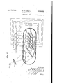
- Figure 1 is a partly diagrammatic perspective View of a multistage electron multiplier provided, in accordance with the principle of our invention.
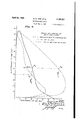
- Figure 2 shows diagrammatically so much of v the device of Fig. 1 as is necessary to explain the contour and the relative arrangement of the Accordingly, the principal object of our present invention is to obviate the above described be apparent and our invention itself will be best electrodes required to" achieve optimum per-1 55 A formance;
- Figure 3 is an explanatory tabulation
- Figure 4 is a diagram which will be referred to in explaining the trajectories of the electrons in a device utilizing the electrode arrangement of Fig. 2.
- the electron multiplier shown in Fig. 1 comprises an evacuated envelope T which, for purposes of this description, may be considered to contain a reference axis AA adjacent the opposite ends of which an anode l3 and an over- 10 size photosensitive cathode C are mounted.
- a pair of sets of curved substantially L-shape multiplying (i. e., secondary-electron emissive) electrodes aremounted on opposite sides of the reference axis between the cathode and anode.
- The, electrodes of the upper set are odd-numbered IM, 3M, 5M, TM and 9M, and those of the .lower.. set are even-numbered 2M, 4M, 6M
- each L-shape multiplying electrode except electrode IM, extends across the axis A-A with its free end inclined toward the cathode.
- 'I'heshort leg of each of the said Ls extends in the direction of the anode and each terminates at a point substantially equally distant from the said reference axis.
- the contour of the cathode C differs from that of the first multiplying electrode IM and the contour of electrode IM preferably, but not necessarily, differs from the contour of the other multiplying electrodes.
- all of the electron emissive electrodes are of cylindrical curved construction and are mounted with the generatrices of their surfaces normal to a plane containing the reference axis A-A.
- the hollow box-like metal mem ber S which forms a continuation of the surface of the cathode is designed to prevent wall charges (on the. glass) fromaffecting themoticn of the photoelectrons in the region where their velocities are low, but may be omitted if desired.
- the potential distribution preferably employed in operating the device of Fig 1 maybe expressed by the mathematical series IV, 2V, 3V, 4V, 5V, EV, etc, where IV is the potential drop between the photosensitive cathode C and the first target or multiplying electrode, and 2V, 3V, l-V, etc., represent the potential drop between the respective succeeding electrodes in pointofelec-
- the cathode C may be connected to the negative terminal of a direct current source exemplified in the drawings by resistor R, and the first multiplying electrode, 1. e., electrode l connected to a point iV somewhat more positive.
- the other electrodes 2 to 9, inclusive, in the order of their numbers, are shown connected to successively more positive points 2V to 9V on the resistor.
- the reference characters IV, 2V, 3V, etc., given to the several points on resistor R will be understood to indicate that the voltage drop between the given electrode and the cathode is the designated whole number multiple of the drop existing between the cathode C and the first multiplying electrode lM.
- the drop between electrodes 2M and C should preferably be 200 volts, that between the electrodes 3M and C, 300 volts.
- a beam of light, say of varying intensity, from a source exemplified by a lamp l is difiused by a lens over substantially the entire surface of the over-size cathode C.
- the quantity of photoelectrons released .by the impress .of the difiused light beam upon the cathode will be, of course, determined by 1 1 6 instantaneous intensity of the light beam.
- These photo-electrons will be accelerated toward the first upper electrode IM and, because of the described design, relative.
- the photo-electrons striking electron lM will cause the emission of secondary electrons, the number of secondary electrons, emitted being dependent, in part at least, upon the magnitude of the potential between it and the cathode.
- the next electrode in point of electron travel is the second lower electrode 2M.
- the trajectory of secondary electrons from the firstv multiplying electrode IM is such that they impinge upon the cupped surface of the second multiplying electrode 2M.
- a multiplication. by reason of secondary emission, is secured, and this is repeated in any number of stages untilthe amplified stream of secondary electrons is col,-
- the electrode plotted in the manner above described, and whose position is determined by the point a, should be considered as the third electrode, in point'of electron travel, from the cathode.
- a distance equal to 1.09R is measured in each direction from it along the axis A-TA and from these points, a, a respectively, duplicate electrodes are plotted on the side of. the axis opposite to electrode 3.
- multiplying electrodes may be provided as are necessary or desirable to achieve a desired degree of amplification.
- first multiplying electrode iii/D measure from a a distance equal to 1.86R along A-.-A, in the cathode direction, and from this point an erect a perpendicular (on the same side of the axis as b) and terminate it at a point J removed 1.293R from the axis.
- To form the first multiplying electrode describe an arc of a radius equal to .8243. about 7. Terminate this are on theanode side at a point 9 such that the angle between of and an. is 86.
- the cathode (C) is finally located by drawing a point 7' on axis A A spaced 4.031% in the negative direction from a, erecting a perpendicular (on the side of the axis opposite to points b and' to point k which is removed 0564B from the A-A.
- the contour of the cathode is determined by describing an arc of a radius equal to 2.731%
- point is; terminating the are, on the posi tive side, at a point m distance 1.583. from the axis AA and on the negative side at a point n 84 removed from point 'm. From point 71. the
- a line drawn between points'i and m should make an angle of 53 with axis :c-ac.
- the relative size and the contour and relative ar-' rangementof the cathode and multiplying electrodes may also be defined by giving the 2), then the coordinates are those given in the table of Fig. 3. It will be seen, from an inspection of Fig. 2, that the cathode is in quadrant III 7 55 tangent to the are at n is drawn in the negative and is defined by a straight line from 11. through 11, and by a circular are drawn between n and m about It as a center.
- the first multiplying electrode IM is defined by a straight line connecting i and h, and by a circular are drawn between h and g about ,1 as a center.
- the third multiplying electrode 3M is defined by a straight line connecting e and d, and by a circular are drawn between d and about I) as a center. Any of the other multiplying electrodes (which, for the sake of convenience, may be designated as the nth multiplying electrode) is described about the point bn congruent to the said third multiplying electrode 3M, and has the same aspect with respect to the Cartesian :c axis.
- the surfaces of the cathode C and the surfaces of the multiplying electrodes IM, 2M and 3M each carries a numbered scale.
- the scale on the cathode is numbered 0 to 13; the scale on the electrode IM from O to 10; and the scales on electrodes 2M and 3M from 0 to 16, respectively.
- the vertical and horizontal numbered scales on the chart of Fig. 4 correspond, as indicated in the legend adjacent respectively thereto, to the scales on the several electrodes of How well the objects of the invention are achieved in an electrode assembly constructed in the manner shown in Fig. 2 is illustrated by the chart of Fig. 4 which shows the relation between the origin and termini of the electron paths between successive electrodes.
- Fig. 4 show that electrons released from any point on the photocathode between. points 0 and 11 will strike electrode IM between the points 0 and 5.5. Secondary electrons leaving electrode IM from any point within this region will strike electrode 2M between points 1 and 11.5. Secondary electrons leaving electrode 2M from any point within. this region will strike electrode 3M between points 0 and 9.
- a photoelectron released from any point on the photocathode will give rise to a group of secondary electrons which will be focused without any munerical diminution upon the next succeeding electrode and thereby give rise to a new and augmented group of secondary-electrons which are, in turn, focused without loss upon the next succeeding multiplying electrode.
- the reading is about i So far in this description we have made no reference to the lateraldimensio-ns of the oathode and multiplying electrodes.
- this dimension i. e. dimension across the long axis A--A of the device
- the width of these electrodes be sufficient to minimize so called
- An electron-multiplier comprising a cathode, an anode and at least three multiplyingelectrodes, said cathode and multiplying electrodes having curved emissive surfaces the generatrices of which are parallel to each other, said cathode surface having a substantially greater emissive area than the first multiplying electrode and said first multiplying electrode having a substantially greater emissive area than the multiplying electrode next adjacent thereto.
- each of the multiplying electrodes following the second multiplying electrode has substantially the same emissive area as said second multiplying electrode.
- An electron multiplier comprising a cylindrical photosensitive cathode, an anode and at least three cylindrical multiplying electrodes mounted on opposite sides of a reference axis which extends between said cathode and anode, the relative size and the contour and relative arrangement of said cathode and multiplying electrodes, as viewed in a plane normal to the generatrices of said cylindrical electrodes, being defined substantially by the points a, b, c, etc., whose Cartesian coordinates are given in the. following table in which the axis of a: coincides with said reference axis and said cathode lies in quadrant III,
- said cathode being defined by a straight line from n through 72 and by a circular are drawn between 11 and m about 7c as a center
- the first multiplying electrode being defined by a straight line connecting i and h and by a circular are drawn between it and 9 about 1 as a center
- the third multiplying electrode being defined by a straight line connecting e and d and by acircular are connecting it and 0 about b as a center
- the nth multiplying electrode being described about the point bn congruent to the said third multiplying electrode and having the same aspect with respect to the said reference axis.
Description
April 23, 1940. E. w. PIKE ET AL ELECTRON MULTIPLIER Filed May :5, 1938 3 Sheets-Sheet 1 w, Jw u memr m wmaw w E eR 9;. an: E m wm April 23, 1940. E. w. PIKE ET AL ELECTRON HULI'IPLIER Filed May 3, 1938 3 Sheets-Sheet 2 9.5 A? 5N6 o m ma R c N kwm o kmx w twm o .556 0 thaws o a INVENTOHS:
m ne m 8 M a Pmd WQJ u Emm J Patented Apr. 23, 1940 ELECTRON MULTHLIER Eugene W. Pike, Swarthmore, and Jan A. Rajchman, Philadelphia, Pa., and Richard L. Snyder, Jr., Glassboro, N. J assignors to Radio Corporation of America,
Delaware a corporation of Application May 3, 1938, Serial No. 205,672
6 Claims.
Our invention relates to electron discharge devices, particularly to photosensitive electronmultipliers and has special reference to the provision of improvements in the photo and first secondary-electron emissive stages of such devices.
The sensitivity of the ordinary photo cathode is usually not perfectly uniform. It is therefore frequently desirable to employ a photo cathode of large area and to diliuse the lightrays impinging thereon so that changes in the light which would otherwise change the point of in and other disadvantages inherent in photosensitive electron-multiplier devices. Another object of our invention is to provide an electrostatic (as distinguished fromvelectromagnetic) type multiplier having an over-size cathode and to determine the particular contour and relative position and arrangement of the electrodes required to achieve optimum performance in an electron multiplier which has been thus modified.
Another and important object of our invention is to provide improvements in electron multipliers of the type described in, copending application 40 Serial No. 171,916, to Rajchmanand Pike, filed October 30, 1937. t
Certain important details of construction,.to gether with other objects and advantages, will 45 understood by referring to the following description and to the accompanying drawings wherein" Figure 1 is a partly diagrammatic perspective View of a multistage electron multiplier provided, in accordance with the principle of our invention,
50 with an over-size photosensitive cathode;
Figure 2 shows diagrammatically so much of v the device of Fig. 1 as is necessary to explain the contour and the relative arrangement of the Accordingly, the principal object of our present invention is to obviate the above described be apparent and our invention itself will be best electrodes required to" achieve optimum per-1 55 A formance;
tron travel, and said cathode.
Figure 3 is an explanatory tabulation; and
Figure 4 is a diagram which will be referred to in explaining the trajectories of the electrons in a device utilizing the electrode arrangement of Fig. 2. v 6
The electron multiplier shown in Fig. 1 comprises an evacuated envelope T which, for purposes of this description, may be considered to contain a reference axis AA adjacent the opposite ends of which an anode l3 and an over- 10 size photosensitive cathode C are mounted. A pair of sets of curved substantially L-shape multiplying (i. e., secondary-electron emissive) electrodes aremounted on opposite sides of the reference axis between the cathode and anode. The, electrodes of the upper set are odd-numbered IM, 3M, 5M, TM and 9M, and those of the .lower.. set are even-numbered 2M, 4M, 6M
and 8M. i
The long leg of each L-shape multiplying electrode, except electrode IM, extends across the axis A-A with its free end inclined toward the cathode. 'I'heshort leg of each of the said Ls extends in the direction of the anode and each terminates at a point substantially equally distant from the said reference axis.
As will hereinafter more fully appear, the contour of the cathode C differs from that of the first multiplying electrode IM and the contour of electrode IM preferably, but not necessarily, differs from the contour of the other multiplying electrodes. However, all of the electron emissive electrodes are of cylindrical curved construction and are mounted with the generatrices of their surfaces normal to a plane containing the reference axis A-A. The hollow box-like metal mem ber S which forms a continuation of the surface of the cathode is designed to prevent wall charges (on the. glass) fromaffecting themoticn of the photoelectrons in the region where their velocities are low, but may be omitted if desired.
The potential distribution preferably employed in operating the device of Fig 1 maybe expressed by the mathematical series IV, 2V, 3V, 4V, 5V, EV, etc, where IV is the potential drop between the photosensitive cathode C and the first target or multiplying electrode, and 2V, 3V, l-V, etc., represent the potential drop between the respective succeeding electrodes in pointofelec- For the purpose of providing such a potential distribution, the cathode C may be connected to the negative terminal of a direct current source exemplified in the drawings by resistor R, and the first multiplying electrode, 1. e., electrode l connected to a point iV somewhat more positive. The other electrodes 2 to 9, inclusive, in the order of their numbers, are shown connected to successively more positive points 2V to 9V on the resistor. The reference characters IV, 2V, 3V, etc., given to the several points on resistor R will be understood to indicate that the voltage drop between the given electrode and the cathode is the designated whole number multiple of the drop existing between the cathode C and the first multiplying electrode lM. Thus, where the potential drop between the first multiplying electrode EM and the cathode C is 100 volts, the drop between electrodes 2M and C should preferably be 200 volts, that between the electrodes 3M and C, 300 volts. In accordance with the invention, a beam of light, say of varying intensity, from a source exemplified by a lamp l is difiused by a lens over substantially the entire surface of the over-size cathode C. The quantity of photoelectrons released .by the impress .of the difiused light beam upon the cathode will be, of course, determined by 1 1 6 instantaneous intensity of the light beam. These photo-electrons will be accelerated toward the first upper electrode IM and, because of the described design, relative.
arrangement and voltage distribution will impinge upon this first multiplying electrode. The photo-electrons striking electron lM will cause the emission of secondary electrons, the number of secondary electrons, emitted being dependent, in part at least, upon the magnitude of the potential between it and the cathode.
The next electrode in point of electron travel is the second lower electrode 2M. The trajectory of secondary electrons from the firstv multiplying electrode IM is such that they impinge upon the cupped surface of the second multiplying electrode 2M. Hereagain, a multiplication. by reason of secondary emission, is secured, and this is repeated in any number of stages untilthe amplified stream of secondary electrons is col,-
lected upon the inclined surface of the anode B. and caused to flow in a utilization circuit exemplified. in the drawings by the impedance Z which is included between the output electrode l3 and the positive terminal lay of the potential divider R. I
The principal difiiculty encountered in. apply ing our inventive concept to multistage electronmultinliers of the type disclosed in the above identified Raichman and Pike application was in the design of an electrode assembly capable of directing all of the electrons from an over-size cathode to the smaller target electrodes without substantial numericaldiminution. By the words over-size cathode we mean a cathodehaving an emissive area at least twice that of the first multiplying electrode. Many arrangements capab e of focusinga substantial percent of the elec trons from an oversize cathode upon the input multiplying electrode are possible. However, after a great many experiments, we have succeeded in designing and constructing an electrode assembly capable of utilizing substantially all of the electrons from an oversize cathode and have formulated the following mode of procedure to enable others skilled in the art to duplicate this desired result. i
Referring now to Fig. 2 and to the chart of Fig. '3: It is first necessary to select a unit of length (R) which determines the scale of the multiplier. 7 By way ofexample, a unit wherein R 0.25 will ensure a device of a convenient size. Now, having drawn the axis A-A and deequal to R, terminate this are on the positive (anode) side at a point .0, at a distance equal to 0.81R from the axis AA, and terminate the other end of the arc at a point cl which lies 12a" in the counter-clockwise direction with respect to c. Now draw a tangent to the are at point 02 and extend it a distance equal to 0.73R to point e,
crossing the axis A--A.
The electrode plotted in the manner above described, and whose position is determined by the point a, should be considered as the third electrode, in point'of electron travel, from the cathode. To locate the second, the fourth and succeeding multiplying electrodes, a distance equal to 1.09R is measured in each direction from it along the axis A-TA and from these points, a, a respectively, duplicate electrodes are plotted on the side of. the axis opposite to electrode 3. Obviously, as many multiplying electrodes may be provided as are necessary or desirable to achieve a desired degree of amplification.
To locate the first multiplying electrode iii/D, measure from a a distance equal to 1.86R along A-.-A, in the cathode direction, and from this point an erect a perpendicular (on the same side of the axis as b) and terminate it at a point J removed 1.293R from the axis. To form the first multiplying electrode, describe an arc of a radius equal to .8243. about 7. Terminate this are on theanode side at a point 9 such that the angle between of and an. is 86. This are is extended in a counter-clockwise directionl1l from 'g to point h, and from h the tangent to the arc-at h is extended in the cathode direction a distance equal to 2.0453. to the point Point 2' thus constitutes one terminal edge and point g the other terminal edge of electrode IM.
The contour and relative arrangement of the multiplying electrodes having been determined. the cathode (C) is finally located by drawing a point 7' on axis A A spaced 4.031% in the negative direction from a, erecting a perpendicular (on the side of the axis opposite to points b and' to point k which is removed 0564B from the A-A. The contour of the cathode is determined by describing an arc of a radius equal to 2.731%
about point is; terminating the are, on the posi tive side, at a point m distance 1.583. from the axis AA and on the negative side at a point n 84 removed from point 'm. From point 71. the
direction to a point p which isremoved from n a distance equal to or greater than 3374B. To check the position of the cathode C with respect to electrode 1M. a line drawn between points'i and m should make an angle of 53 with axis :c-ac.
From the foregoing, it will be apparent that the relative size and the contour and relative ar-' rangementof the cathode and multiplying electrodes, as viewed in a plane normal to the generatrices of the cylindrical (curved) electrodes (as in 2) may also be defined by giving the 2), then the coordinates are those given in the table of Fig. 3. It will be seen, from an inspection of Fig. 2, that the cathode is in quadrant III 7 55 tangent to the are at n is drawn in the negative and is defined by a straight line from 11. through 11, and by a circular are drawn between n and m about It as a center.
The first multiplying electrode IM is defined by a straight line connecting i and h, and by a circular are drawn between h and g about ,1 as a center. The third multiplying electrode 3M is defined by a straight line connecting e and d, and by a circular are drawn between d and about I) as a center. Any of the other multiplying electrodes (which, for the sake of convenience, may be designated as the nth multiplying electrode) is described about the point bn congruent to the said third multiplying electrode 3M, and has the same aspect with respect to the Cartesian :c axis.
Referring again to Fig. 2. It will be observed that the surfaces of the cathode C and the surfaces of the multiplying electrodes IM, 2M and 3M each carries a numbered scale. Thus, the scale on the cathode is numbered 0 to 13; the scale on the electrode IM from O to 10; and the scales on electrodes 2M and 3M from 0 to 16, respectively. The vertical and horizontal numbered scales on the chart of Fig. 4 correspond, as indicated in the legend adjacent respectively thereto, to the scales on the several electrodes of How well the objects of the invention are achieved in an electrode assembly constructed in the manner shown in Fig. 2 is illustrated by the chart of Fig. 4 which shows the relation between the origin and termini of the electron paths between successive electrodes.
By way of example, the path of a photo-electron released from a point (say point 4) on the cathode, will be traced. Referring to the vertical scale of Fig. 4 and projecting a line at right angles from point 4 on the said scale to the point ti on the broken line curve and reading this point (ti) on the horizontal scale, it will be seen that the said electron will strike electrode 5M near point 3 on that electrode.
Assume now that a secondary electron is released at the point of impact, i. e., point 3; then to ascertain where on electrode 2M this secondary-electron will strike it is merely necessary to move vertically from point 151 to point t2 on. the solid-line curve and to read the point 152 on the vertical scale. 5.2, which means that the said secondary electron will strike electrode 2M about point 5.2.
Proceeding similarly from point 152 to point is on the clot and dash curve and projecting point ts on the horizontal scale, it will be seenthat an electron released from. point is on. electrode 2M will strike electrode 3M at about point 7.7 on that electrode.
The curves of Fig. 4 show that electrons released from any point on the photocathode between. points 0 and 11 will strike electrode IM between the points 0 and 5.5. Secondary electrons leaving electrode IM from any point within this region will strike electrode 2M between points 1 and 11.5. Secondary electrons leaving electrode 2M from any point within. this region will strike electrode 3M between points 0 and 9. Thus, a photoelectron released from any point on the photocathode will give rise to a group of secondary electrons which will be focused without any munerical diminution upon the next succeeding electrode and thereby give rise to a new and augmented group of secondary-electrons which are, in turn, focused without loss upon the next succeeding multiplying electrode.
end effects.
of the several electrodes is preferably ten times In this case the reading is about i So far in this description we have made no reference to the lateraldimensio-ns of the oathode and multiplying electrodes. In practice, this dimension (i. e. dimension across the long axis A--A of the device) is relatively unimportant, the only requirement is that the width of these electrodes be sufficient to minimize so called As a matter of practice, the width the R of Fig. 2 thus if R=0.25 the width of the cathode and multiplying electrodes will preferably be substantially no less than 2.5 inches.
It will be understood that the foregoing is to be interpreted as illustrative and not in a limiting sense except as required by the prior art and by the spirit of the appended claims.
What is claimed is:
1. An electron-multiplier comprising a cathode, an anode and at least three multiplyingelectrodes, said cathode and multiplying electrodes having curved emissive surfaces the generatrices of which are parallel to each other, said cathode surface having a substantially greater emissive area than the first multiplying electrode and said first multiplying electrode having a substantially greater emissive area than the multiplying electrode next adjacent thereto.
'2. The invention as set forth in claim 1 and wherein each of the multiplying electrodes following the second multiplying electrode has substantially the same emissive area as said second multiplying electrode.
3. An electron multiplier comprising a cylindrical photosensitive cathode, an anode and at least three cylindrical multiplying electrodes mounted on opposite sides of a reference axis which extends between said cathode and anode, the relative size and the contour and relative arrangement of said cathode and multiplying electrodes, as viewed in a plane normal to the generatrices of said cylindrical electrodes, being defined substantially by the points a, b, c, etc., whose Cartesian coordinates are given in the. following table in which the axis of a: coincides with said reference axis and said cathode lies in quadrant III,
said cathode being defined by a straight line from n through 72 and by a circular are drawn between 11 and m about 7c as a center, the first multiplying electrode being defined by a straight line connecting i and h and by a circular are drawn between it and 9 about 1 as a center, the third multiplying electrode being defined by a straight line connecting e and d and by acircular are connecting it and 0 about b as a center, the nth multiplying electrode being described about the point bn congruent to the said third multiplying electrode and having the same aspect with respect to the said reference axis.
4. The invention as set forth in claim 3 wher in R is equal to substantially one-quarter of an inch.
5. The invention as set forth in claim 3 Whereinthe-widthof said electrndesasmeasumd across in the angle abc is substantially 124, the angle said referenees-axisis substantially no less than cbd is substantially 125, the angle gfal is sub- 10R. stantially 86, the angle gfh is substantially 111, the angle mic is substantially 117 and the angle mlm is substantially 84.
6. The invention as set forth in claim 3 Where- EUGENE W. PIKE. JAN A. RAJCI-IMAN. RICHARD L. SNYDER, JR.
Priority Applications (2)
| Application Number | Priority Date | Filing Date | Title |
|---|---|---|---|
| US205672A US2198227A (en) | 1938-05-03 | 1938-05-03 | Electron multiplier |
| GB12426/39A GB527996A (en) | 1938-05-03 | 1939-04-25 | Improvements in or relating to electron multiplier tubes |
Applications Claiming Priority (1)
| Application Number | Priority Date | Filing Date | Title |
|---|---|---|---|
| US205672A US2198227A (en) | 1938-05-03 | 1938-05-03 | Electron multiplier |
Publications (1)
| Publication Number | Publication Date |
|---|---|
| US2198227A true US2198227A (en) | 1940-04-23 |
Family
ID=22763166
Family Applications (1)
| Application Number | Title | Priority Date | Filing Date |
|---|---|---|---|
| US205672A Expired - Lifetime US2198227A (en) | 1938-05-03 | 1938-05-03 | Electron multiplier |
Country Status (2)
| Country | Link |
|---|---|
| US (1) | US2198227A (en) |
| GB (1) | GB527996A (en) |
Cited By (2)
| Publication number | Priority date | Publication date | Assignee | Title |
|---|---|---|---|---|
| US2553197A (en) * | 1941-06-25 | 1951-05-15 | Hartford Nat Bank & Trust Co | Photoelectric tube |
| US3239709A (en) * | 1962-06-26 | 1966-03-08 | Rca Corp | Electron multiplier having electrostatic field shaping electrodes |
-
1938
- 1938-05-03 US US205672A patent/US2198227A/en not_active Expired - Lifetime
-
1939
- 1939-04-25 GB GB12426/39A patent/GB527996A/en not_active Expired
Cited By (2)
| Publication number | Priority date | Publication date | Assignee | Title |
|---|---|---|---|---|
| US2553197A (en) * | 1941-06-25 | 1951-05-15 | Hartford Nat Bank & Trust Co | Photoelectric tube |
| US3239709A (en) * | 1962-06-26 | 1966-03-08 | Rca Corp | Electron multiplier having electrostatic field shaping electrodes |
Also Published As
| Publication number | Publication date |
|---|---|
| GB527996A (en) | 1940-10-21 |
Similar Documents
| Publication | Publication Date | Title |
|---|---|---|
| US2793319A (en) | Electron lens structure for television tubes | |
| US3496406A (en) | Cathode ray tubes with electron beam deflection amplification | |
| US2908840A (en) | Photo-emissive device | |
| US1929067A (en) | Frequency multiplier | |
| US2237671A (en) | Electron discharge device | |
| US2198227A (en) | Electron multiplier | |
| US2230134A (en) | Image analyzing tube | |
| US2837689A (en) | Post acceleration grid devices | |
| US2203048A (en) | Shielded anode electron multiplier | |
| US2147756A (en) | Secondary electron tube | |
| US3082342A (en) | Photo-electric tube | |
| US2868994A (en) | Electron multiplier | |
| US2231682A (en) | Electron multiplier | |
| US2131563A (en) | Cathode ray tube | |
| US2585798A (en) | Beam deflection tube amplifier | |
| US2473031A (en) | Electron multiplier for ultra high frequencies | |
| US2285126A (en) | Electron multiplier | |
| US2272232A (en) | Electron beam tube | |
| US2172738A (en) | Cathode ray tube | |
| US3054019A (en) | Television and like camera tubes | |
| US3109115A (en) | Magnetron type ionization gauges | |
| US2227062A (en) | Electron discharge device | |
| US3772551A (en) | Cathode ray tube system | |
| US2900559A (en) | Double stream growing-wave amplifier | |
| US2260613A (en) | Electron multiplier |